

Features
•
2-Wire Serial Interface
•
Schmitt Trigger, Filtered Inputs For Noise Suppression
•
DDC1™/ DDC2™ Interface Compliant for Monitor Identification
•
Low Voltage Operatio n
– 2.5 (VCC = 2.5V to 5.5V)
•
Internally Organized 128 x 8
•
100 kHz (2.5V) Compatibility
•
8-Byte Page Write Mode
•
Write Protection Available
•
Self-timed Write Cycle (10 ms max)
•
High Reliability
– Endurance: 1 Million Write Cycles
– Data Retention: 100 Years
– ESD Protection: >3000V
•
8-Pin PDIP and JEDEC SOIC Packages
Description
The AT24C21 provides 1024 bits of serial electrically erasable and programmable
read only memory (EEPROM) organized as 128 words of 8 bits each. The device is
optimized for use in applications requiring data storage and serial transmission of configuration and control information. The AT24C21 features two modes of operation:
Transmit-Only Mode and Bi directio nal Mode. Upo n power- up, the AT24C21 will be in
the Transmit-Only Mode, sending a serial-bit stream of the entire m emory contents,
clocked via the VCLK pin. The Bidirect ional Mode is selected by a val id high-to-low
transition on the SCL pi n an d off ers b yte sel ect able read /wri te c apab ility of the enti re
memory array. The A T24C2 1 i s av ailab le in s pac e sa vi ng 8-pi n PDIP a nd 8- pi n S OIC
packages.
2-Wire Serial
EEPROM
1K (128 x 8)
AT24C21
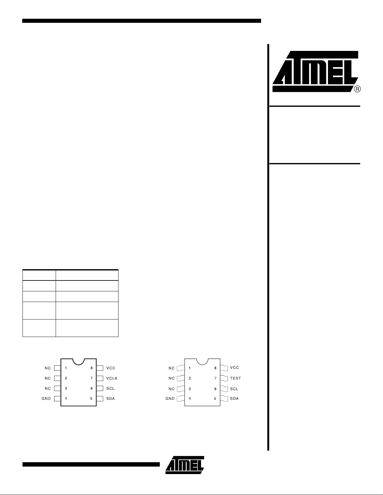
Pin Configurations
Pin Name Function
NC No Connect
SDA Serial Data
SCL Serial Clock Input
(Bidirectional Mode)
VCLK Serial Clock Input
(Transmit-Only Mode)
8-Pin PDIP 8-Pin SOIC
2-Wire, 1K
Serial EEPROM
Rev. 0405E–07/98
1
Absolute Maximum Ratings*
Operating Temperature................................. -55°C to +125°C
Storage Temperature .................................... -65°C to +150°C
Voltage on Any Pin
with Respect to Ground.....................................-1.0V to +7.0V
Maximum Operating Voltage........................................... 6.25V
DC Output Current........................................................5.0 mA
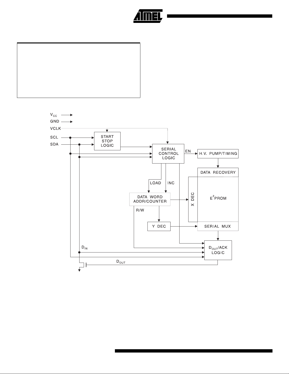
Block Diagram
*NOTICE: Stresses beyond those listed under “Absolute
Maximum Ratings” may cause permanent damage to the dev ice . This is a s tress rating only an d
functional oper ation of the device at thes e or any
other conditions beyond those indicated in the
operational sections of this specification is not
implied. Exposure to absolute maximum rating
conditions f or e xtended periods ma y af fect de vice
reliability .
Pin Description
SERIAL CLOCK (SCL):
edge clock data into each EEPROM device and negative
edge clock data out of each device.
SERIAL DATA (SDA):
serial data transfer. This pin is open-drain driven and may
be wire-ORed with any number of other open drain or open
collector devices.
2
The SCL input is used to positive
The SDA pin is bidirectional for
AT24C21
SERIAL CLOCK (VCLK):
the Transmit-Only mode and will transmit the entire memory contents via the SDA pin with positive signals on the
VCLK pin.
Upon power-up, the device is in
Memory Organization
AT24C21, 1K SERIAL EEPROM:
128 pages of one byte each. The 1K requires a 7-bit data
word address for random word addressing.
Internally organized wi th
AT24C21
DC Characteristics
Applicable ov er recommen ded operat ing range from: TAI = -40°C to +85°C, TAC = 0°C to +70°C, VCC = +2.5V to +5.5V
(unless otherwise noted).
Symbol Parameter Test Condition Min Typ Max Units
V
CC
I
CC
I
CC
I
SB
I
LI
I
LO
V
IL
V
IH
V
OL
Supply Voltage 2.5 5.5 V
Supply Current VCC = 5.0V READ at 100 KHz 0.4 1.0 mA
Supply Current VCC = 5.0V WRITE at 100 KHz 2.0 3.0 mA
Standby Current .......VCC = 2.5V
.......VCC = 5.0V
Input Leakage Current VIN = VCC or V
Output Leakage Current V
Input Low Level
(1)
SCL, SDA Pin
Input Low Level VCLK Pin VCC ≥ 2.7V
Input High Level
(1)
SCL, SDA Pin
Input High Level VCLK Pin
VIN = VCC or V
VIN = VCC or V
= VCC or V
OUT
V
< 2.7V
CC
SS
SS
SS
SS
3.0
12.0
0.10 1.0
0.05 1.0
-0.6 V
VCC × 0.7
2.0
4.0
30.0
× 0.3
CC
0.8
0.2 × V
CC
VCC + 0.5 V
Output Low Level VCC = 3.0V IOL = 2.1 mA 0.40 V
Note: 1. VIL min and VIH max are for reference only and not tested.
Pin Capacitance
(1)
Applicable over recommended operating range from TA = 25°C, f = 1.0 MHz, VCC = +1.8V.
Symbol Test Condition Max Units Conditions
C
I/O
C
IN
Note: 1. This parameter is characterized and is not 100% tested.
Input/Out put Capacitance (SDA) 8 pF V
I/O
= 0V
Input Capacitance (A0, A1, A2, SCL, VCLK) 6 pF VIN = 0V
µ
A
µ
A
µ
A
µ
A
V
V
V
V
Transmit-Only Mode
Symbol Parameter 2.5-volt Units
Min Max
T
T
T
T
T
VAA
VHIGH
VLOW
VHZ
VPU
Output valid from VCLK 500 ns
VCLK high-time 4.0
VCLK low-time 4.7
Mode transition time 500 ns
Transmit-Only power-up time 0 ns
µ
s
µ
s
3

AC Characteristics
Applicable over recommended operating range from TA = -40°C to +85°C, VCC = +2.5V to +5.5V CL = 1 TTL Gate and
100 pF (unless otherwise noted).
2.5-volt
Symbol Parameter
f
SCL
t
LOW
t
HIGH
t
I
Clock Frequency, SCL 0 100 KHz
Clock Pulse Width Low 4.7
Clock Pulse Width High 4.0
Noise Suppression Time
(1)
(SDA and SCL pins)
t
t
AA
BUF
Clock Low to Data Out Valid 0.1 3.5
Time the bus must be free before a new
transmission can start
t
HD.STA
t
SU.STA
t
HD.DAT
t
SU.DAT
t
R
t
F
t
SU.STO
t
DH
t
WR
Endurance
(1)
Start Hold Time 4.0
Start Set-up Time 4.7
Data In Hold Time 0
Data In Set-up Time 250 ns
Inputs Rise Time
Inputs Fall Time
(1)
(1)
Stop Set-up Time 4.0
Data Out Hold Time 100 ns
Write Cycle Time 10 ms
5.0V, 25°C, Page Mode 1M Write Cycles
Note: 1. This parameter is characterized and is not 100% tested.
4.7
UnitsMin Max
µ
µ
NA ns
µ
µ
µ
µ
µ
1.0
µ
300 ns
µ
s
s
s
s
s
s
s
s
s
4
AT24C21

Functional Description
The AT24C21 has two mode s of operation: the T ransmitOnly Mode and the Bidirectional Mode. There is a separate
2-wire protocol to support eac h mod e, eac h havi ng a se parate clock input (SCL and VCLK) and both modes sharing a
common Bidirectional data line (SDA). The AT24C21
enters the Transmit-Only Mode upon po wering up the
device. In this m ode, th e d ev ice tra ns mi ts dat a o n t he SDA
pin upon a clock signal on the VCLK pin. The device will
remain in the Transmit-Only Mode until a valid high-to-low
transition takes place o n the SCL pin. The devi ce will
switch into the Bidirectional Mode when a valid transition
on the SCL pin is recognized. Once the device has transitioned to the Bidirectional Mode, there is no way to return to
the Transmit-Onl y Mo de, e xcep t to power down (res et) the
device.
Transmit-Only Mode (DDC1)
The AT24C21 will power up in the Transmit-Only Mode. In
this mode, the device will output one bit of data on the SDA
pin on each r ising edge on the V CL K pin. D ata is tra nsmitted in 8 bit words with the most s ignificant bit first. Eac h
AT24C21
word is followed by a 9th “don't care” bit whic h will be in
high impedance state (ref er to Fi gur e 1). The A T24 C21 will
continuously cycle through the entire memory array in
incremental sequence as long a VCLK is present and no
falling edges on SCL are received. When the maximum
address (7FH) is reached, the output will wrap around to
the zero location (00H) and continue. The Bidirectiona l
mode clock (SCL) pin must be hel d high for the devic e to
remain in the Transmit-Only mod e.
Upon power-up, the AT24C21 will not output valid data until
it has been initialized. During initialization, data will not be
available until after the first nine clocks are sent to the
device (refer to Figu re 2). The starting addr ess for the
Transmit-Only mode can be determined during initiali zation. If the SDA p in is h eld hi gh du ring the first eight cloc ks
(refer to Figure 2), the starting address will be 7FH. If the
SDA pin is low during the first eight clocks, the starting
address will be 00H. During the ninth clock, SDA should be
in high impedance.
Figure 1.
Figure 2.
Transmit-Only Mode
Device Initialization for Transmit-Only Mode
5

Bidirectional Mode (DDC2)
This mode supp orts a 2-wi re, Bidi rectional data tr ansmission protocol. The AT24C21 can be switched into the Bidirectional Mode by issui ng a valid high to low transition o n
the SCL pin (refer to Figure 3). After the device is in the
Bidirectional Mode, all inputs to the VCLK pin are ignored,
except when a logic high is required to enable write capability. All byte and page writes and byte and sequential
reads are supported in this mode.
Bidirectional Mode Operation
CLOCK and DATA TRANSITIONS:
mally pulled high wi th an ex ter na l dev ic e. Dat a o n t he SDA
pin may chan ge o nly duri ng S CL l ow t ime per iods (refe r t o
Data Validity timing diagram). Data changes during S CL
high periods will indicate a start or stop condition as
defined below.
START CONDITION:
SCL high is a start condition which must precede any other
command (refer to Start and Stop Definition timing diagram).
STOP CONDITION:
SCL high is a stop condition. After a read or write
sequence, the stop command will place the EEPROM in a
standby power mode (refer to Start and Stop Definition timing diagram).
ACKNOWLEDGE:
ally transmitted to and from the EEPROM in 8-bit words.
The EEPROM sends a zero to acknowledge th at it has
A high-to-low transition of SDA wi th
A low-to-high transition of SDA with
All addresses and data words are seri-
The SDA pin is nor-
received each word. This happens during the ninth clock
cycle.
Device Addressing
The AT24C21 requires an 8-bit device address word following a start condition to enable the chip for a read or
write operation (refer to Figure 4).
The device address word consists of a mandatory one,
zero sequence for th e first four most si gnificant bits as
shown. This is common to all the EEPROM devices.
The next three bits are don’t care for the AT24C21.
The eighth bit of the device address is the read/write opera-
tion select b it. A read operat ion is initia ted if th is bit is high
and a write operation is initiated if this bit is low.
Upon a compare of the device address, the EEPROM will
output a zero. If a compar e is not made, the chip will return
to a standby state.
STANDBY MODE:
standby mode which is enabled: (a) upon power-up and (b)
after the receipt of the STOP bit and the completi on of any
internal operations.
MEMORY RESET:
loss or system reset, any 2-wire part can be reset by following these steps:
(a) Clock up to 9 cycles, (b) look for SDA high in each cycle
while SCL is high and then (c) create a start condition as
SDA is high.
The AT24C21 features a l ow power
After an interruption in protocol, power
Figure 3.
Mode Transition
6
AT24C21

Bus Timing
SCL: Serial Clock, SDA: Serial Data I/O
Write Cycle Timing
SCL: Serial Clock, SDA: Serial Data I/O
AT24C21
SCL
SDA
Note: 1. The write cycle time tWR is the time from a valid stop condition of a write sequence to the end of the internal clear/write
cycle.
8th BIT ACK
WORD n
STOP
CONDITION
t
(1)
WR
START
CONDITION
7

Data Validity
Start and Stop Definition
Output Acknowledge
8
AT24C21

AT24C21
Write Operations
BYTE WRITE:
word addresses following the device address word and
acknowledgment. U pon receipt of this address, the
EEPROM will again respond with a zero and then clock in
the first 8-bit data word. Following receipt of the 8-bit data
word, the EEPROM will output a zero and the addr essing
device, such as a mi croc ontr olle r, mus t ter min ate the w rit e
sequence with a stop condition. At this time the EEPROM
enters an internally-timed write cycle , t
tile memory. All inputs are disabled during this write cycle
and the EEPROM will not respond until the write is complete (refer to Figure 5).
It is required that VCLK be held at a high logic level in order
to program the device. This applies to byte write and page
write operation. Note th at VCLK can go low while the
device is in its self-timed program operation and not affect
programming.
PAGE WRITE:
write.
A page write is ini tiated the same as a byte wri te, but the
microcontroller does not send a stop condition after the first
data word is clocked in. Instead, after the EEPROM
acknowledges receipt of the first data word, the microcontroller can transmit up to seven more data words. The
EEPROM will respond with a zero after each data word
received. Th e microcontr oller must ter minate the pag e
write sequence with a stop condition (refer to Figure 6).
The data word address lower thre e bit s are in ter nal ly inc r emented following the rece ipt of each data word. The hig her
data word address bits ar e not incremen ted, retaini ng the
memory page row location. When the word address, internally generated, reaches the page boundary, the following
byte is placed at the beginning of the same page. If more
than eight data words are transmit ted to the EEPRO M, the
data word address will “roll over” and previous data will be
overwritten. The addres s “rol l ove r” durin g writ e is fro m the
last byte of the current page to the first byte of the same
page.
It is required that VCLK be held at a high logic level in order
to program the device. This applies to byte write and page
write operation. Note th at VCLK can go low while the
device is in its self-timed program operation and not affect
programming.
ACKNOWLEDGE POLLING:
write cycle has started and the EEPROM inputs are disabled, acknowledge polling can be initiated. T his invol ves
sending a start condition followed by the device address
word. The read/write bit is repres entative of the operation
desired. Only if the internal write cycle has completed will
the EEPROM respond with a zero allowing the read or
write sequence to continue.
A write operation requi res an 8-bit data
, to the nonvola-
WR
The AT24C21 is capable of an 8-b yte page
Once the internally-time d
WRITE PROTECTION:
GND and in the Bidirectional Mode, the entire memory is
protected and becomes ROM only. This protects the device
memory from any inadvertent write operations.
NOISE PROTECTION:
the SDA and SCL pins prevent small noise spikes from
activating the device. Furthermore, the AT24C21 employs
a low V
logic whenever V
detector circuit which disables the erase\wri te
CC
CC
When VCLK pin is connected to
Special internal circuitry placed on
falls below 1.5 volts.
Read Operations
Read operations are initiated the same way as write operations with the exception that the read/write select bit in the
device address word is set to one. There are t hree read
operations: current address read, random address read
and sequential read.
CURRENT ADDRESS REA D:
address counter maintains the last address accessed during the last read or write operation, incremented by one.
This address stays valid between operations as long as the
chip power is maintained. T he address “roll over” during
read is from the last byte of the last memory page to the
first byte of the first page.
Once the device address with the read/wr ite select b it set
to one is clocked in and acknowledged by the EEPROM,
the current address data word is s erially clo cked out. The
microcontroller does not respond with an input zero but
does generate a following stop condition (refer to Figure 7).
RANDOM READ:
write sequence to load i n the data wo rd addr ess. Once th e
device address word and data word address are clocked in
and acknowledge d by the EE PROM, the microcontroll er
must generate another start condition. The microcontroller
now initiates a current address read by sending a device
address with the read/write select b it high. The EEP ROM
acknowledges the device address and serially clocks out
the data word. The microcontroller does not respond with a
zero but does generate a following stop condition (refer to
Figure 8).
SEQUENTIAL READ:
either a current address read or a random address read.
After the microcontroller receives a data word, it responds
with an acknowledge. As long as the EEPROM receives an
acknowledge, it will continue to increment the data word
address and serially clock out sequential data words. When
the memory address limit is reached, the data word
address will “roll over” and the sequential read will continue. The sequential r ead operation is terminated when
the microcontroller does not respond with a zero but does
generate a following stop condition (refer to Figure 9).
A random read require s a “dummy ” byte
Sequential reads are initiated by
The internal data word
9

Figure 4.
Device Address
Figure 5.
Figure 6.
Figure 7.
Byte Write
Page Write
(*=Don’t care bits)
Current Address Read
Figure 8.
10
Random Read
AT24C21

AT24C21
Figure 9.
Sequential Read
(*=Don’t care bits)
11

Ordering Information
tWR (max)
(ms)
10 3000 4 100 AT24C21-10PC-2.5
ICC (max)
(µA)
3000 4 100 AT24C21-10PI-2.5
ISB (max)
(µA)
f
MAX
(KHz) Ordering Code Package Operation Range
AT24C21-10SC-2.5
AT24C21-10SI-2.5
8P3
8S1
8P3
8S1
Commercial
(0°C to 70°C)
Industrial
(-40°C to 85°C)
Package Type
8P3 8-Lead, 0.300" Wide, Plastic Dual Inline Package (PDIP)
8S1 8-Lead, 0.150" Wide, Plastic Gull Wing Small Outline (JEDEC SOIC)
Options
-2.5 Low-Voltage (2.5V to 5.5V)
12
AT24C21

Packaging Information
AT24C21
8P3
, 8-Lead, 0.300” Wide, Plastic Dual Inline
Package (PDIP)
Dimensions in Inches and (Millimeters)
JEDEC STANDARD MS-001 BA
.400 (10.16)
.355 (9.02)
PIN
1
.280 (7.11)
.240 (6.10)
.037 (.940)
.300 (7.62) REF
.210 (5.33) MAX
SEATING
PLANE
.150 (3.81)
.115 (2.92)
.012 (.305)
.008 (.203)
.070 (1.78)
.045 (1.14)
.027 (.690)
.100 (2.54) BSC
.015 (.380) MIN
.022 (.559)
.014 (.356)
.325 (8.26)
.300 (7.62)
0
REF
15
.430 (10.9) MAX
8S1
, 8-Lead, 0.150” Wide, Plastic Gull Wing Small
Outline (JEDEC SOIC)
Dimension in Inches and (Millimeters)
.020 (.508)
.013 (.330)
.244 (6.20)
.228 (5.79)
.068 (1.73)
.053 (1.35)
.010 (.254)
.007 (.203)
PIN 1
0
8
.157 (3.99)
.150 (3.81)
.050 (1.27) BSC
.196 (4.98)
.189 (4.80)
.010 (.254)
.004 (.102)
REF
.050 (1.27)
.016 (.406)
13
 Loading...