

Features
•
Low Voltage and Standard Voltage Operation
– 5.0 (VCC = 4.5V to 5.5V)
– 2.7 (VCC = 2.7V to 5.5V)
– 2.5 (VCC = 2.5V to 5.5V)
– 1.8 (VCC = 1.8V to 5.5V)
•
Internally Organized 2048 x 8 (16K)
•
2-Wire Serial Interface
•
Schmitt Trigger, Filtered Inputs for Noise Suppression
•
Bidirectional Data Transfer Protocol
•
100 KHz (1.8V, 2.5V, 2.7V) and 400 KHz (5V) Compatibility
•
Write Protect Pin for Hardware Data Protection
•
Cascadable Feature Allows for Extended Densities
•
16-Byte Page Wri te Mode
•
Partial Page Writes Are Allowed
•
Self-Timed Write Cycle (10 ms max)
•
High Reliability
– Endurance: 1 Million Write Cycles
– Data Retention: 100 Years
– ESD Protection: >3,000V
•
Automotive Grade and Extended Temperature Devices Available
•
8-Pin JEDEC SOIC and 8-Pin PDIP Packages
Description
The AT24C164 provides 16,38 4 bits of serial electricall y erasable and programma ble
read only memory (EEPROM) organized as 2048 words of 8 bits each. The device’s
cascadable feature allows up to eight devices to share a common 2-wire bus. The
device is optimiz ed for use in ma ny in dustria l and co mmerci al app lica tions where low
power and low voltage operation are essential. The AT24C164 is available in space
saving 8-pin PDIP and 8-pin SOIC packages and is accessed via a 2-wire serial interface. In addition, this device is available in 5.0V (4.5V to 5.5V), 2.7V (2.7V to 5.5V),
2.5V (2.5V to 5.5V) and 1.8V (1.8V to 5.5V) versions.
2-Wire Serial
EEPROM
16K (2048 x 8)
AT24C164
Pin Configurations
Pin Name Function
A0 to A2 Address Inputs
SDA Serial Data
SCL Serial Clock Input
WP Write Protect
8-Pin PDIP
A0
A1
A2
GND
1
2
3
4
8
7
6
5
VCC
WP
SCL
SDA
A0
A1
A2
GND
8-Pin SOIC
1
2
3
4
2-Wire, 16K
Serial EEPROM
VCC
8
WP
7
SCL
6
SDA
5
Rev. 0105D–07/98
1
Absolute Maximum Ratings*
Operating Temperature.................................. -55°C to +125°C
Storage Temperature..................................... -65°C to +150°C
Voltage on Any Pin
with Respect to Ground.....................................-1.0V to +7.0V
Maximum Operating Voltage........................................... 6.25V
DC Output Current........................................................5.0 mA
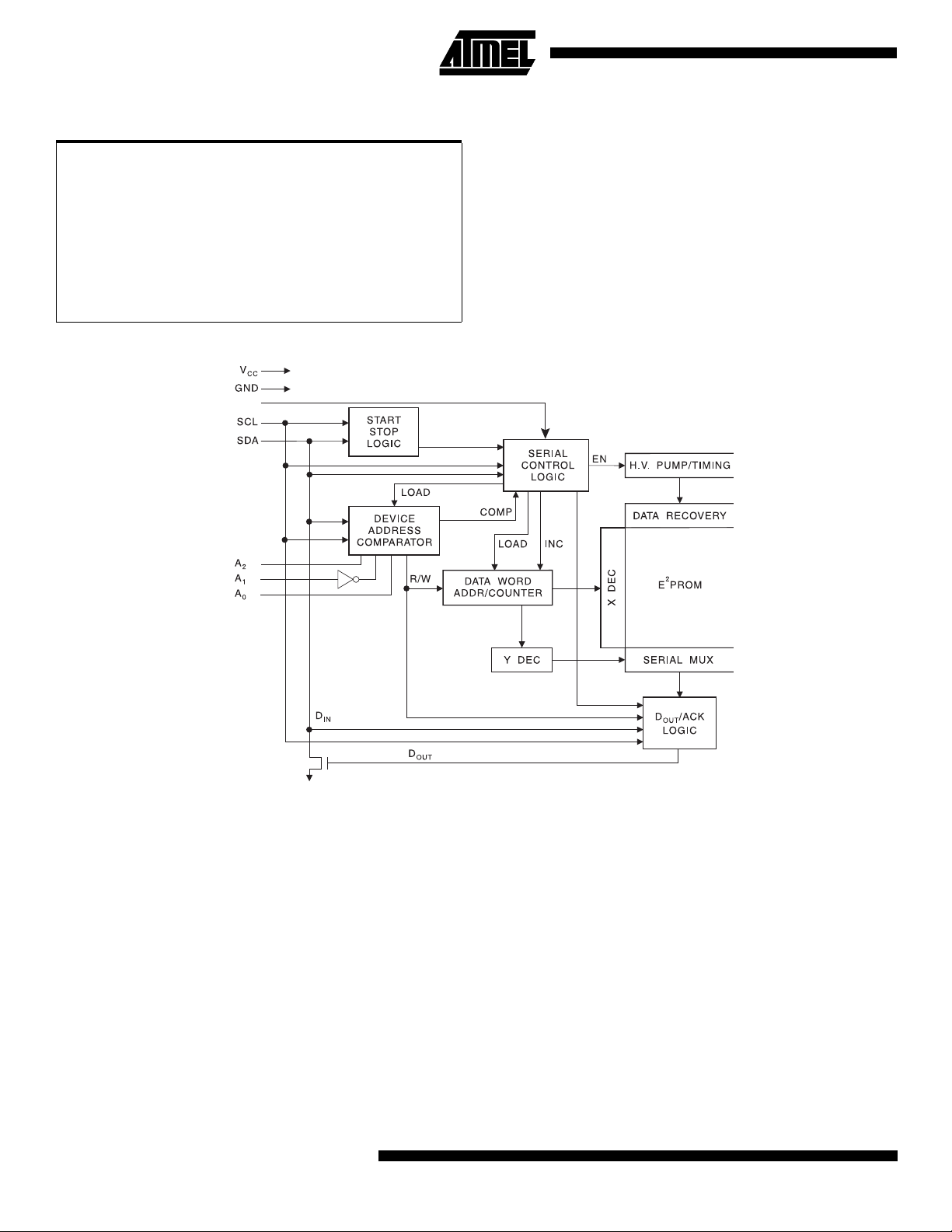
Block Diagram
WP
*NOTICE: Stresses beyond those listed under “Absolute
Maximum Ratings” may cause permanent damage to the dev ice . This is a s tress rating only an d
functional oper ation of the device at these or an y
other conditions beyond those indicated in the
operational sections of this specification is not
implied. Exposure to absolute maximum rating
conditions f or e xtended periods ma y af fect de vice
reliability .
Pin Description
SERIAL CLOCK (SCL):
edge clock data into each EEPROM device and negative
edge clock data out of each device.
SERIAL DATA (SDA ):
serial data transfer. This pin is open-drain driven and may
be wire-ORed with any number of other open-drain or open
collector devices.
DEVICE SELECT (A2, A1, A0):
are device address inputs that may be hardwired or actively
driven to V
2
or VSS. These inputs allow the sel ection for
DD
The SCL input is used to positive
The SDA pin is bidirectional for
The A2, A1 and A0 pins
AT24C164
one of eight possible devices sharing a common bus. The
AT24C164 can be made compatible with the AT24C16 by
tying A2, A1 and A0 to V
in detail in the device addressing section.
WRITE PROTECT (WP):
low to GND, allows normal write operations.
. Device addressing is discussed
SS
The write protect input, when tied
Memory Organization
The AT24C164 is internally organized with 256 pages of
8 bytes each. Random word addressing requires an 11 bit
data word address.
AT24C164
Pin Capacitance
(1)
Applicable over recommended operating range from TA = 25°C, f = 1.0 MHz, VCC = +1.8V.
Symbol T est Conditi on Max Units Conditions
C
I/O
C
IN
Input/Output Capacitance (SDA) 8 pF V
I/O
= 0V
Input Capacitance (A0, A1, A2, SCL) 6 pF VIN = 0V
Note: 1. This parameter is characterized and is not 100% tested.
DC Characteristics
Applicable over recommended operating range from: TAI = -40°C to +85°C, VCC = +1.8V to +5.5V, TAC = 0°C to +70°C,
= +1.8V to +5.5V (unless otherwise noted).
V
CC
Symbol Parameter Test Condition Min Typ Max Units
V
CC1
V
CC2
V
CC3
V
CC4
I
CC
I
CC
I
SB1
I
SB2
I
SB3
I
SB4
I
LI
I
LO
V
IL
V
IH
V
OL2
V
OL1
Note: 1. V
Supply Voltage 1.8 5.5 V
Supply Voltage 2.5 5.5 V
Supply Voltage 2.7 5.5 V
Supply Voltage 4.5 5.5 V
Standby Current VCC = 5.0V READ at 100 KHz 0.4 1.0 mA
Standby Current VCC = 5.0V WRITE at 100 KHz 2.0 3.0 mA
Standby Current VCC = 1.8V VIN = VCC or V
Standby Current VCC = 2.5V VIN = VCC or V
Standby Current VCC = 2.7V VIN = VCC or V
Standby Current VCC = 5.0V VIN = VCC or V
Input Leakage Current VIN = VCC or V
Output Leakage Current V
Input Low Level
Input High Level
(1)
(1)
OUT = VCC
or V
SS
SS
SS
SS
SS
SS
-0.6 VCC x 0.3 V
VCC x 0.7 VCC + 0.5 V
0.6 3.0
1.4 4.0
1.6 4.0
8.0 18.0
0.10 3.0
0.05 3.0
Output Low Level VCC = 3.0V IOL = 2.1 mA 0.4 V
Output Low Level VCC = 1.8V IOL = 0.15 mA 0.2 V
min and VIH max are reference only and are not tested.
IL
µ
A
µ
A
µ
A
µ
A
µ
A
µ
A
3

AC Characteristics
Applicable over recomme nded operating r ange from TA = -40°C to +85°C, VCC = +1.8V to +5.5V, CL = 1 TTL Gate and
100 pF (unless otherwise noted).
2.7-, 2.5-, 1.8-volt 5.0-volt
Symbol Parameter
f
SCL
t
LOW
t
HIGH
t
I
t
AA
t
BUF
t
HD.STA
t
SU.STA
t
HD.DAT
t
SU.DAT
t
R
t
F
t
SU.STO
t
DH
t
WR
Endurance
Notes: 1. This parameter is characterized and is not 100% tested.
(1)
Clock Frequency, SCL 100 400 KHz
Clock Pulse Width Low 4.7 1.2
Clock Pulse Width High 4.0 0.6
Noise Suppression Time
Clock Low to Data Out Valid 0.1 4.5 0.1 0.9
Time the bus must be free before a new
transmission can start
Start Hold Time 4.0 0.6
Start Set-up Time 4.7 0.6
Data In Hold Time 0 0
Data In Set-up Time 200 100 ns
Inputs Rise Time
Inputs Fall Time
Stop Set-up Time 4.7 0.6
Data Out Hold Time 100 50 ns
Write Cycle Time 10 10 ms
5.0V, 25°C, Page Mode 1M 1M Write
(1)
(1)
(1)
(1)
100 50 ns
4.7 1.2
1.0 0.3
300 300 ns
UnitsMin Max Min Max
µ
s
µ
s
µ
s
µ
s
µ
s
µ
s
µ
s
µ
s
µ
s
cycles
Device Operation
CLOCK and DATA TRANSITIONS:
mally pulled high wi th an ex ter na l dev ic e. Dat a o n t he SDA
pin may chan ge o nly duri ng S CL l ow t ime per iods (refe r t o
Data Validity timing diagram). Data changes during S CL
high periods will indicate a start or stop condition as
defined below.
START CONDITION:
A high-to-low transition of SDA with
SCL high is a start condition which must precede any other
command (refer to Start and Stop Definition timing diagram).
STOP CONDITION:
A low-to-high transition of SDA with
SCL high is a stop condition. After a read sequence, the
stop command will pla ce the EEPR OM in a standb y power
mode (refer to Start and Stop Definition timing diagram).
4
AT24C164
The SDA pin is nor-
ACKNOWLEDGE:
All addresses and data words are serially transmitted to and from the EEPROM in 8-bit words.
The EEPROM sends a zero to acknowledge that it has
received each word. This happens during the ninth clock
cycle.
STANDBY MODE:
The AT24C164 features a low power
standby mode which is enabled: a) upon power-up and b)
after the receipt of the STOP bit and the completi on of any
internal operations.
MEMORY RESET:
After an interruption in protocol, power
loss or system reset, the AT24C164 can be reset by following these steps:
(a) Clock up to 9 cycles, (b) look for SDA high in each cycle
while SCL is high and then (c) create a start condition as
SDA is high.

Bus Timing
SCL: Serial Clock, SDA: Serial Data I/O
Write Cycle Timing
SCL: Serial Clock, SDA: Serial Data I/O
AT24C164
(1)
Note: 1. The write cycle time tWR is the time from a valid stop condition of a write sequence to the end of the internal clear/write
cycle.
5

Data Validity
Start and Stop Definition
Output Acknowledge
6
AT24C164

AT24C164
Device Addressing
The AT24C164 requires an 8-bit device address word following a start condi tion to en able th e chip for read or writ e
operations (refer to Figure 1) . The most sign ifica nt bit must
be a one followed by the A2, A1 and A0 device select bits
(the A1 bit must be the compliment of the A1 input pin signal). The next 3 bits are used for memory block addressing
and select one of the eight 256 x 8 memory blocks. These
bits should be consid ered the thr ee most s ignif icant bi ts of
the data w o rd ad d re ss . T he ei gh t h b it o f t h e de vi ce ad dress
is the read/w rite s elec t bit. A rea d oper ation is s elect ed if
this bit is high or a write oper ation is sel ected if this bit is
low.
Upon a compare of the device address, the EEPROM will
output a zero. If a compare is not m ade , the c hip wi ll r et ur n
to a standby state.
Write Operations
BYTE WRITE:
word address following the device address word and
acknowledgment. U pon receipt of this address, the
EEPROM will again respond with a zero and then clock in
the first 8-bit data word. Following receipt of the 8-bit data
word, the EEPROM will output a zero and the addr essing
device, such as a mi croc ontr olle r, mus t ter min ate the w rit e
sequence with a stop condition. At this time the EEPROM
enters an internally-timed write cycle, t
memory. All inputs are disabled during this write cycle and
the EEPROM will not respond until the writ e is complete
(refer to Figure 2).
PAGE WRITE:
page write. A page write is initiated the same as a byte
write, but the microco ntroller does not send a stop co ndition after the first data word is cloc ked in . Instead, afte r the
EEPROM acknowledges receipt of the first data word, the
microcontroll er can trans mit up to fi fteen mo re data wo rds.
The EEPROM will respond with a zero after each data
word received. The microcontroller must terminate the
page write sequence with a stop condition (refer to Figure
3).
The data word address lower 4 bits are internally incre-
mented following the rece ipt of each data word. The hig her
data word address bits are not incremented retaining the
memory page row location. When the word address, internally generated, reaches the page boundary, the following
byte is placed at the beginning of the same page. If more
than sixteen d ata wor ds are transmi tted to the EEPROM ,
the data word address will “roll ov er” and previ ous data will
be overwritten.
A write operation requi res an 8-bit data
, to the nonvolatile
WR
The AT24C164 is capable of a 16-byte
ACKNOWL EDGE POLLING:
write cycle has started and the EEPROM inpu ts are disabled, acknowledge polling can be initia ted. This invol ves
sending a start condition followed by the device address
word. The read/write bit is repres entative of the oper ation
desired. Only if the internal wri te cycle has c ompleted will
the EEPROM respon d with a zero allowing the read or
write sequence to continue.
Once the internally-time d
Read Operations
Read operations are initiated the same way as write operations with the exception that the read/write select bit in the
device address word is set to one. There are t hree read
operations: current address read, random address read
and sequential read.
CURRENT ADDRESS REA D:
address counter maintains the last address accessed during the last read or write operation, incremented by one.
This address stays valid between operations as long as the
chip power is maintained. T he address “roll over” during
read is from the last byte of the last memory page to the
first byte of the first page. The address “roll over” during
write is from the last byte of the current page to first byte of
the same page.
Once the device address with the read/wr ite select b it set
to one is clocked in and acknowledged by the EEPROM,
the current address data word is s erially clo cked out. The
microcontroller does not respond with an input zero but
does generate a following stop condition (refer to Figure 4).
RANDOM READ:
write sequence to load i n the data wo rd addr ess. Once th e
device address word and data word address are clocked in
and acknowledge d by the EE PROM, the microcontroll er
must generate another start condition. The microcontroller
now initiates a current address read by sending a device
address with the read/write select b it high. The EEP ROM
acknowledges the device address and serially clocks out
the data word. The microcontroller does not respond with a
zero but does generate a following stop condition (refer to
Figure 5).
SEQUENTIAL READ:
either a current address read or a random address read.
After the microcontroller receives a data word, it responds
with an acknowledge. As long as the EEPROM receives an
acknowledge, it will continue to increment the data word
address and serially clock out sequential data words. When
the memory address limit is reached, the data word
address will “roll over” and the sequential read will continue. The sequential r ead operation is terminated when
the microcontroller does not respond with a zero but does
generate a following stop condition (refer to Figure 6).
A random read require s a “dummy ” byte
Sequential reads are initiated by
The internal data word
7

Figure 1.
Device Address
Figure 2.
Figure 3.
Figure 4.
Byte Write
Page Write
Current Address Read
Figure 5.
8
Random Read
AT24C164

AT24C164
Figure 6.
Sequential Read
9

Ordering Information
tWR (max)
(ms)
10 3000 18 400 AT24C164-10PC
10 1500 4 100 AT24C164-10PC-2.7
10 1000 4 100 AT24C164-10PC-2.5
10 800 4 100 AT24C164-10PC-1.8
ICC (max)
(µA)
3000 18 400 AT24C164-10PI
1500 4 100 AT24C164-10PI-2.7
1000 4 100 AT24C164-10PI-2.5
800 4 100 AT24C164-10PI-1.8
ISB (max)
(µA)
f
MAX
(KHz) Ordering Code Packa ge Operation Range
AT24C164-10SC
AT24C164-10SI
AT24C164-10SC-2.7
AT24C164-10SI-2.7
AT24C164-10SC-2.5
AT24C164-10SI-2.5
AT24C164-10SC-1.8
AT24C164-10SI-1.8
8P3
8S1
8P3
8S1
8P3
8S1
8P3
8S1
8P3
8S1
8P3
8S1
8P3
8S1
8P3
8S1
Commercial
(0°C to 70°C)
Industrial
(-40°C to 85°C)
Commercial
(0°C to 70°C)
Industrial
(-40°C to 85°C)
Commercial
(0°C to 70°C)
Industrial
(-40°C to 85°C)
Commercial
(0°C to 70°C)
Industrial
(-40°C to 85°C)
Package Type
8P3 8 Lead, 0.300" Wide, Plastic Dual Inline Package (PDIP)
8S1 8 Lead, 0.150" Wide, Plastic Gull Wing Small Outline Package (JEDEC SOIC)
Options
Blank Standard Operation (4.5V to 5.5V)
-2.7 Low-Voltage (2.7V to 5.5V)
-2.5 Low-Voltage (2.5V to 5.5V)
-1.8 Low-Voltage (1.8V to 5.5V)
10
AT24C164

Packaging Information
AT24C164
8P3
, 8-Lead, 0.300” Wide, Plastic Dual Inline
Package (PDIP)
Dimensions in Inches and (Millimeters)
JEDEC STANDARD MS-001 BA
.400 (10.16)
.355 (9.02)
PIN
1
.280 (7.11)
.240 (6.10)
.037 (.940)
.300 (7.62) REF
.210 (5.33) MAX
SEATING
PLANE
.150 (3.81)
.115 (2.92)
.012 (.305)
.008 (.203)
.070 (1.78)
.045 (1.14)
.027 (.690)
.100 (2.54) BSC
.015 (.380) MIN
.022 (.559)
.014 (.356)
.325 (8.26)
.300 (7.62)
0
REF
15
.430 (10.9) MAX
8S1
, 8-Lead, 0.150” Wide, Plastic Gull Wing Small
Outline (JEDEC SOIC)
Dimensions in Inches and (Millimeters)
.020 (.508)
.013 (.330)
.244 (6.20)
.228 (5.79)
.068 (1.73)
.053 (1.35)
.010 (.254)
.007 (.203)
PIN 1
0
8
.157 (3.99)
.150 (3.81)
.050 (1.27) BSC
.196 (4.98)
.189 (4.80)
.010 (.254)
.004 (.102)
REF
.050 (1.27)
.016 (.406)
11
 Loading...