

ATMEL AT24C256-10PC-1.8, AT24C256-10PC, AT24C256-10CI-2.7, AT24C256-10CI-1.8, AT24C256-10CI Datasheet
...
1
Features
•
Low Voltage and Standard Voltage Operation
– 5.0 (VCC = 4.5V to 5.5V)
– 2.7 (VCC = 2.7V to 5.5V)
– 1.8 (VCC = 1.8V to 3.6V)
•
Internally Organized 16,384 x 8 and 32,768 x 8
•
2-Wire Serial Interface
•
Schmitt Trigger, Filtered Inputs for Noise Suppression
•
Bidirectional Data Transfer Protocol
•
1 MHz (5V), 400 kHz (2.7V) and 100 kHz (1.8V) Compatibility
•
Write Protect Pin for Hardware and Software Data Protection
•
64-Byte Page Write Mode (Partial Page Writes Allowed)
•
Self-Timed Write Cycle (5 ms typical)
•
High Reliability
– Endurance: 100,000 Write Cycles
– Data Retention: 40 Years
– ESD Protection: > 4000V
•
Automotive Grade and Extended Temperature Devices Available
•
8-Pin JEDEC PDIP, 8-Pin JEDEC and EIAJ SOIC, 14-Pin TSSOP, and
8-Pin Leadless Array Packages
Description
The AT24C128/256 provides 131,072/262,144 bits of serial electrically erasable and
programmable read onl y mem ory ( EEPROM ) organi zed as 16,384/ 32,768 w ords of 8
bits each. The device’s cascadable feature allows up to 4 devices to share a common
2-wire bus. The device is optimized for use in many industrial and commercial applications where low power and low voltage operation are essential. The devices are available in space-saving 8-pin JEDEC PDIP, 8-pin EIAJ, 8-pin JEDEC SOIC, 14-pin
TSSOP, and 8-pin LAP packages. In addition, the entire family is available in 5.0V
(4.5V to 5.5V), 2.7V (2.7V to 5.5V) and 1.8V (1.8V to 3.6V) versions.
Rev. 0670C–08/98
2-Wire Serial
EEPROMs
128K (16,384 x 8)
256K (32,768 x 8)
AT24C128
AT24C256
Pin Configurations
Pin Name Function
A
0
to A
1
Address Inputs
SDA Serial Data
SCL Serial Clock Input
WP Write Protect
NC No Connect
8-Pin PDIP
1
2
3
4
8
7
6
5
A0
A1
NC
GND
VCC
WP
SCL
SDA
8-Pin SOIC
1
2
3
4
8
7
6
5
A0
A1
NC
GND
VCC
WP
SCL
SDA
8-Pin Leadless Array
Bottom View
1
2
3
4
8
7
6
5
VCC
WP
SCL
SDA
A0
A1
NC
GND
14-Pin TSSOP
1
2
3
4
5
6
7
14
13
12
11
10
9
8
A0
A1
NC
NC
NC
NC
GND
VCC
WP
NC
NC
NC
SCL
SDA
AT24C128/256
2
Absolute Maximum Ratings*
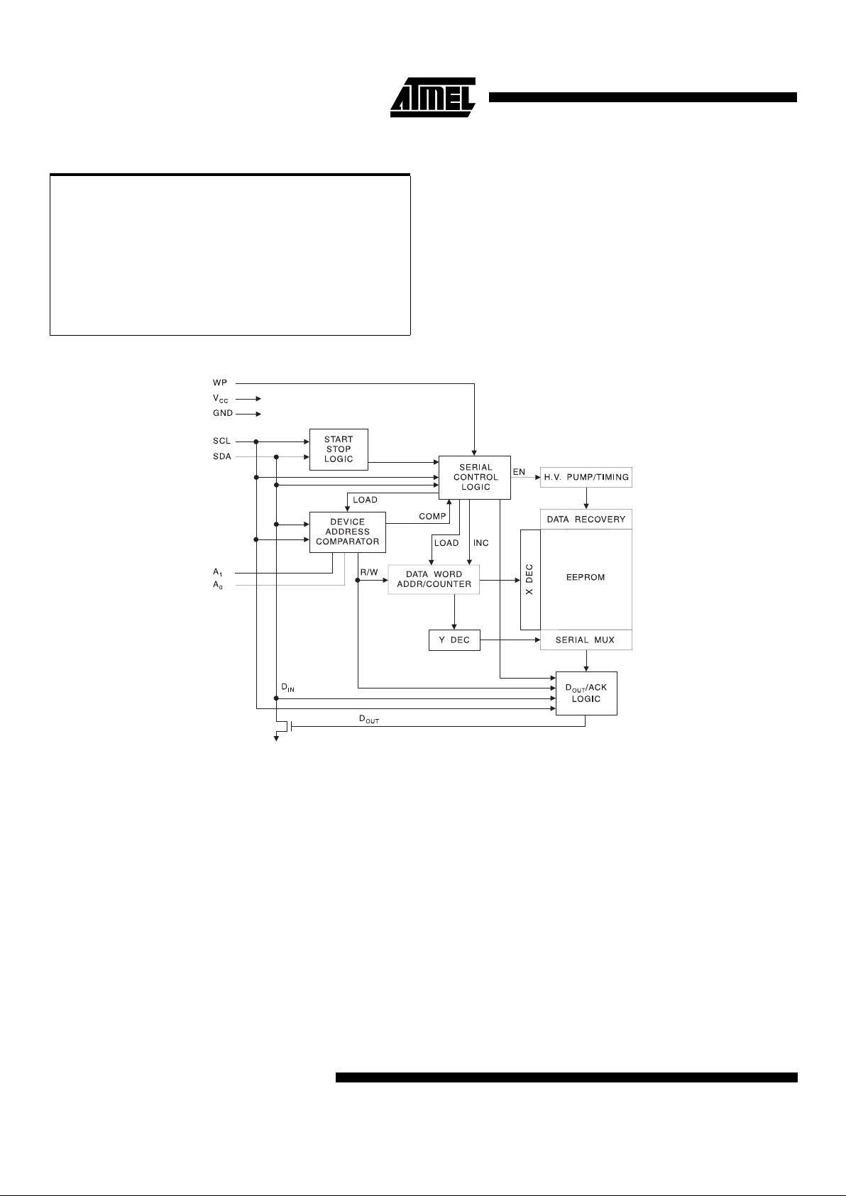
Block Diagram
Pin Description
SERIAL CLOCK (SCL):
The SCL input is used to positive
edge clock data into each EEPROM device and negative
edge clock data out of each device.
SERIAL DATA (SDA):
The SDA pin is bidirectional for
serial data transfer. This pin is open-drain driven and may
be wire-ORed with any number of other open-drain or open
collector devices.
DEVICE/PAGE ADDRESSES (A1, A0):
The A1 and A0
pins are device address inputs that are hardwired or left not
connected for hardware compatibility with AT24C32/64.
When the pins are hardwired, as many as four 128K/256K
devices may be addresse d on a sing le bus system (devic e
addressing is discussed in detail under the Device
Addressing section). When the pins are not hardwired, the
default A
1
and A0 are zero.
WRITE PROTECT (WP):
The write protect input, when tied
to GND, allows normal write operations. Wh en WP is tied
high to V
CC
, all write operations to the memory are inhibited. If left unconnected, WP is interna lly pulled down to
GND. Switching WP to V
CC
prior to a write oper ation cre-
ates a software write protect function.
Memory Organization
AT24C128/256, 128K/256K SERIAL EEPROM:
The
128K/256K is internal ly organ ized as 25 6/512 pag es of 64bytes each. Random word addressing requires a 14/15-bit
data word address.
Operating Temperature.................................. -55°C to +125°C
*NOTICE: Stresses beyond those listed under “Absolute
Maximum Ratings” may cause permanent damage to the dev ice. This is a stress ratin g only an d
functional oper ati on of the device at these or any
other conditions beyond those indicated in the
operational sections of this specification is not
implied. Exposure to absolute maximum rating
conditions f or extende d periods may af fect de vice
reliability.
Storage Temperature.....................................-65°C to +150°C
Voltage on Any Pin
with Respect to Ground.....................................-1.0V to +7.0V
Maximum Operating Voltage........................................... 6.25V
DC Output Current........................................................5.0 mA
AT24C128/256
3
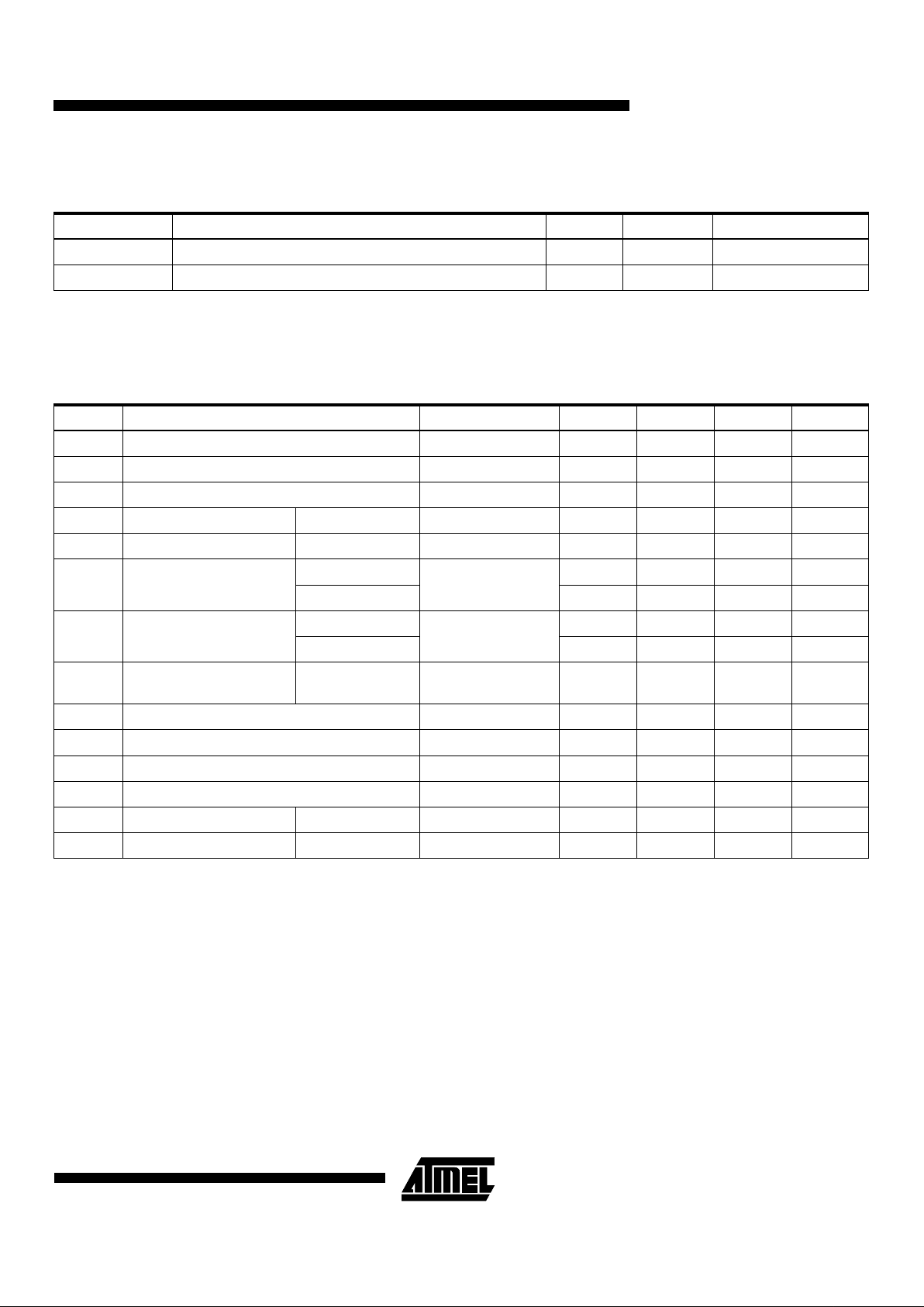
Pin Capacitance
(1)
Applicable over recommended operating range from TA = 25°C, f = 1.0 MHz, VCC = +1.8V.
Note: This parameter is characterized and is not 100% tested.
DC Characteristics
Applicable over recommended operating range from: T
AI
= -40°C to +85°C, VCC = +1.8V to +5.5V, TAC = 0°C to +70°C,
V
CC
= +1.8V to +5.5V (u nless otherwise noted).
Note: VIL min and VIH max are reference only and are not tested
Symbol Test Condition Max Units Conditions
C
I/O
Input/Output Capacitance (SDA) 8 pF V
I/O
= 0V
C
IN
Input Capacitance (A0, A1, SCL) 6 pF VIN = 0V
Symbol Parameter Test Condition Min Typ Max Units
V
CC1
Supply Voltage 1.8 3.6 V
V
CC2
Supply Voltage 2.7 5.5 V
V
CC3
Supply Voltage 4.5 5.5 V
I
CC1
Supply Current VCC = 5.0V READ at 400 kHz 1.0 2.0 mA
I
CC2
Supply Current VCC = 5.0V WRITE at 400 kHz 2.0 3.0 mA
I
SB1
Standby Current
(1.8V option)
V
CC
= 1.8V
V
IN
= VCC or V
SS
0.2
µ
A
V
CC
= 3.6V 2.0
I
SB2
Standby Current
(2.7V option)
V
CC
= 2.7V
V
IN
= VCC or V
SS
0.5
µ
A
VCC = 5.5V 6.0
I
SB3
Standby Current
(5.0V option)
V
CC
= 4.5 - 5.5V VIN = VCC or V
SS
6.0
µ
A
I
LI
Input Leakage Current VIN = V
CC or VSS
0.10 3.0
µ
A
I
LO
Output Leakage Current V
OUT
= V
CC or VSS
0.05 3.0
µ
A
V
IL
Input Low Level
(Note:)
-0.6 VCC x 0.3 V
V
IH
Input High Level
(Note:)
VCC x 0.7 VCC + 0.5 V
V
OL2
Output Low Level VCC = 3.0V IOL = 2.1 mA 0.4 V
V
OL1
Output Low Level VCC = 1.8V IOL = 0.15 mA 0.2 V
AT24C128/256
4
AC Characteristics
Applicable over recom me nded operating range from TA = -40°C to +85°C, VCC = +1.8V to +5.5V, CL = 100 pF (unless otherwise noted). Test conditions are listed in Note 2.
Notes: 1. This parameter is characterized and is not 100% tested.
2. AC measurement conditions:
R
L
(connects to VCC): 1.3KΩ (2.7V, 5V), 10KΩ (1.8V)
Input pulse voltages: 0.3V
CC
to 0.7V
CC
Input rise and fall times: ≤50ns
Input and output timing reference voltages: 0.5V
CC
Device Operation
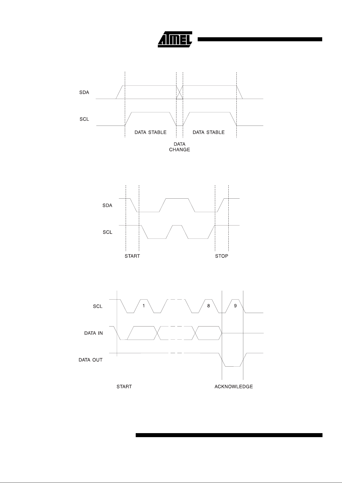
CLOCK and DATA TRANSITIONS:
The SDA pin is normally pulled h ig h w ith an external device . D ata on the SDA
pin may chan ge o nly dur ing SC L lo w ti me p eri ods ( re fer to
Data Validity timing diagram). Data changes during SCL
high periods will indicate a start or stop condition as defined
below.
START CONDITION:
A high-to-low transition of SDA with
SCL high is a start condition which must precede any other
command (refer to Start and Stop Definition timing diagram).
STOP CONDITION:
A low-to-high transition of SDA with
SCL high is a stop condition. After a read sequence, the
stop command will place the EEPROM in a standby power
mode (refer to Start and Stop Definition timing diagram).
ACKNOWLEDGE:
All addresses and data words are serially transmitted to and from the EEPROM in 8-bit words.
The EEPROM sends a zero during the ninth clock cycle to
acknowledge that it has received each word.
STANDBY MODE:
The AT24C128/256 features a low
power standby mode which is enabled: a) upon power-up
and b) after the rec ei pt of t he S T OP bit a nd th e co mpl eti on
of any internal operations.
MEMORY RESET:
After an interruption in protocol, power
loss or system reset, any 2-wire part can be reset by following these steps: (a) Clock up to 9 cycles, (b) look for SDA
high in each cycle while SCL is high and then (c) create a
start condition as SDA is high.
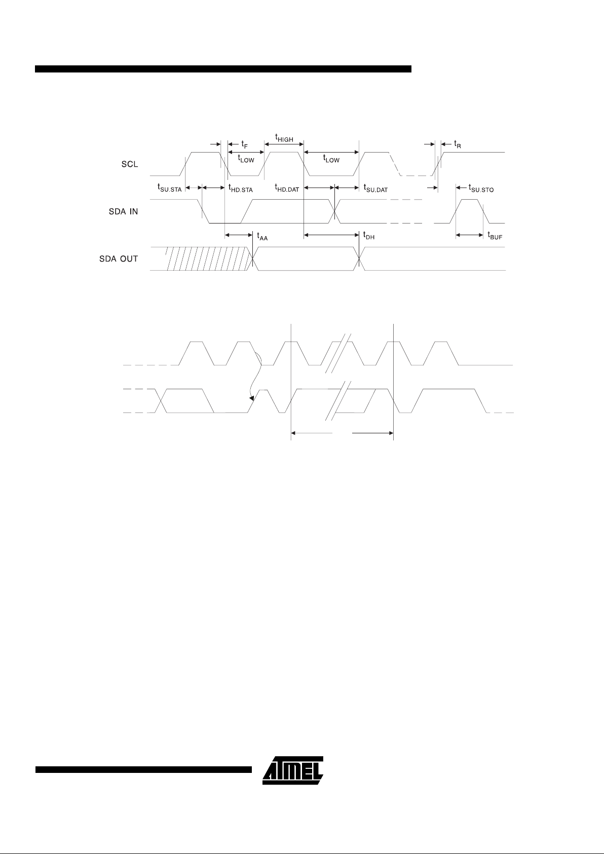
Symbol Parameter
1.8-volt 2.7-volt 5.0-volt
Units
MinMaxMinMaxMinMax
f
SCL
Clock Frequency, SCL 100 400 1000 kHz
t
LOW
Clock Pulse Width Low 4.7 1.3 0.6
µ
s
t
HIGH
Clock Pulse Width High 4.0 1.0 0.4
µ
s
t
AA
Clock Low to Data Out Valid 0.1 4.5 0.05 0.9 0.05 0.55
µ
s
t
BUF
Time the bus must be free before a new
transmission can start
(1)
4.7 1.3 0.5
µ
s
t
HD.STA
Start Hold Time 4.0 0.6 0.25
µ
s
t
SU.STA
Start Set-up Time 4.7 0.6 0.25
µ
s
t
HD.DAT
Data In Hold Time 0 0 0
µ
s
t
SU.DAT
Data In Set-up Time 200 100 100 ns
t
R
Inputs Rise Time
(1)
1.0 0.3 0.3
µ
s
t
F
Inputs Fall Time
(1)
300 300 100 ns
t
SU.STO
Stop Set-up Time 4.7 0.6 0.25
µ
s
t
DH
Data Out Hold Time 100 50 50 ns
t
WR
Write Cycle Time 20 10 10 ms
Endurance
(1)
5.0V, 25°C, Page Mode 100K 100K 100K
Write
Cycles
AT24C128/256
5
Bus Timing (SCL: Serial Clock, SDA: Serial Data I/O)
Write Cycle Timing (SCL: Serial Clock, SDA: Serial Data I/O)
Note: 1. The write cycle time tWR is the time from a valid stop condition of a write sequence to the end of the internal clear/write
cycle.
SCL
SDA
STOP
CONDITION
START
CONDITION
ACK
t
WR
(1)
8th BIT
WORD n
AT24C128/256
6
Data Validity
Start and Stop Definition
Output Acknowledge

AT24C128/256
7
Device Addressing
The 128K/256K EEPROM re qui re s an 8-bit device address
word following a start condition to enable the chip for a read
or write operation (refer to Figure 1). The device address
word consists of a manda tory one , zero s equence for th e
first five most significant bits as shown. This is common to
all 2-wire EEPROM devices.
The 128K/256K uses the two devic e add ress bits A1, A0 to
allow as many as four devices on the same bus. These bits
must compare to their corresponding hardwired input pins.
The A1 and A0 pins use an internal proprietary circuit that
biases them to a lo gic low co nditio n if the pi ns are al lowed
to float.
The eighth bit of the device address is the read/write operation select bit. A read operation is initiated if this bit is high
and a write operation is initiated if this bit is low.
Upon a compare of the device address, the EEPROM will
output a zero. If a compare is not made, the device will
return to a standby state.
DATA SECURITY:
The AT24C128/256 has a hardwa re
data protection scheme that allows the user to write protect
the whole memory when the WP pin is at V
CC
.
Write Operations
BYTE WRITE:
A write operation requires two 8-bit data
word addresses following the device address word and
acknowledgment. U pon receipt of this address, the
EEPROM will again respond with a zero and then clock in
the first 8-bit data word. Following receipt of the 8- bit data
word, the EEPROM will output a zero. The addressing
device, such as a microcontroller, then must terminate the
write sequence with a stop condition. At this time the
EEPROM enters an in ternall y-tim ed write cyc le, t
WR
, to the
nonvolatile memory. All inputs are disabled during this
write cycle and the EEPROM will not respond until the write
is complete (refer to Figure 2).
PA GE WRITE:
The 128K/256K EEPROM is capabl e of 64-
byte page writes.
A page write is initiated the same way as a byte write, but
the microcontroller doe s not s en d a s to p c ond iti on a fter th e
first data word is clocked in. Instead, after the EEPROM
acknowledges receipt of the first data word, the microcontroller can transmit up to 63 more data words. The
EEPROM will respond with a zero after each data word
received. The microcontroller must terminate the page
write sequence with a stop condition (refer to Figure 3).
The data word address lower 6 bits are internally incremented following the rece ipt of e ac h da ta wo rd . The h ig her
data word address bits ar e not incremen ted, retaini ng the
memory page row location. When the word address, internally generated, reaches the page boundary, the following
byte is placed at the beginning of the same page. If more
than 64 data words are transmitted to the EEPROM, the
data word address will “roll over” and previous data will be
overwritten. The address “roll over” during write is from the
last byte of the current page to the first byte of the same
page.
ACKNOWLEDGE POLLING:
Once the internally-timed
write cycle has started and the EEPROM inpu ts are disabled, acknowledge polling can be initiated. This involves
sending a start condition followed by the device address
word. The read/write bit is representati ve of the operati on
desired. Only if the internal write cycle has completed will
the EEPROM respond with a zero, allowing the read or
write sequence to continue.
Read Operations
Read operations are initiated the same way as write operations with the exception that the read/write select bit in the
device address word is set to one. There are t hree read
operations: current address read, random address read
and sequential read.
CURRENT ADDRESS REA D:
The internal data word
address counter maintains the last address accessed during the last read or write operation, incremented by one.
This address stays valid between operations as long as the
chip power is maintained. T he address “roll ov er” during
read is from the last by te of the last memo ry page, to th e
first byte of the first page.
Once the device address with the read/write select b it set
to one is clocked in and acknowledged by the EEPROM,
the current address data word is serially clocked out. The
microcontroller does not respond with an input zero but
does generate a following stop condition (refer to Figure 4).
RANDOM READ:
A random read require s a “dummy ” byte
write sequence to load in t he data wo rd addr ess. Once th e
device address word and data word address are clocked in
and acknowledged by the EE PROM, the mi crocontroll er
must generate another start co nditi on. The mi crocon troller
now initiates a current address read by sending a device
address with the read/write select bit high. The EEPROM
acknowledges the device address and serially clocks out
the data word. The microcontroller does not respond with a
zero but does generate a following stop condition (refer to
Figure 5).
SEQUENTIAL READ:
Sequential reads are initiated by
either a current address read or a random address read.
After the microcontroller receives a data word, it responds
with an acknowledge. As long as the EEPROM receives an
acknowledge, it will continue to increment the data word
address and serially clock out sequential data words. When
the memory address limit is reached, the data word
address will “roll over” and the sequential read will continue. The sequential read operation is terminated when
the microcontroller does not respond with a zero but does
generate a following stop condition (refer to Figure 6).

AT24C128/256
8
Figure 1.
Device Address
Figure 2.
Byte Write
Figure 3.
Page Write
(* = DON’T CARE bit)
(† = DON’T CARE bit for the 128K)
Figure 4.
Current Address Read

AT24C128/256
9
Figure 5.
Random Read
(* = DON’T CARE bit)
(† = DON’T CARE bit for the 128K)
Figure 6.
Sequential Read

AT24C128/256
10
AT24C128 Ordering Information
tWR (max)
(ms)
ICC (max)
(µµµµA)
ISB (max)
(µµµµA)
f
MAX
(kHz) Ordering Code Package Operation Range
10 3000 6.0 1000 AT24C128-10PC
AT24C128N-10SC
AT24C128W-10SC
AT24C128-10CC
AT24C128C1-10CC
AT24C128T1-10TC
8P3
8S1
8S2
8C
8C1
14T
Commercial
(0°C to 70°C)
3000 6.0 1000 AT24C128-10PI
AT24C128N-10SI
AT24C128W-10SI
AT24C128-10CI
AT24C128C1-10CI
AT24C128T1-10TI
8P3
8S1
8S2
8C
8C1
14T
Industrial
(-40°C to 85°C)
10 1500 0.5 400 AT24C128-10PC-2.7
AT24C128N-10SC-2.7
AT24C128W-10SC-2.7
AT24C128-10CC-2.7
AT24C128C1-10CC-2.7
AT24C128T1-10TC-2.7
8P3
8S1
8S2
8C
8C1
14T
Commercial
(0°C to 70°C)
1500 0.5 400 AT24C128-10PI-2.7
AT24C128N-10SI-2.7
AT24C128W-10SI-2.7
AT24C128-10CI-2.7
AT24C128C1-10CI-2.7
AT24C128T1-10TI-2.7
8P3
8S1
8S2
8C
8C1
14T
Industrial
(-40°C to 85°C)
Package Type
8C 8-Lead, 0.230" Wide, Leadless Array Package (LAP)
8C1 8-Lead, 0.300" Wide, Leadless Array Package (LAP)
8P3 8-Lead, 0.300" Wide, Plastic Dual Inline Package (PDIP)
8S1 8-Lead, 0.150" Wide, Plastic Gull Wing Small Outline Package (JEDEC SOIC)
8S2 8-Lead, 0.200" Wide, Plastic Gull Wing Small Outline Package (EIAJ SOIC)
14T 14-Lead, 0.170" Wide, Thin Shrink Small Outline Package (TSSOP)
Options
Blank Standard Operation (4.5V to 5.5V)
-2.7 Low-Voltage (2.7V to 5.5V)
-1.8 Low-Voltage (1.8V to 3.6V)

AT24C128/256
11
20 800 0.2 100 AT24C128-10PC-1.8
AT24C128N-10SC-1.8
AT24C128W-10SC-1.8
AT24C128-10CC-1.8
AT24C128C1-10CC-1.8
AT24C128T1-10TC-1.8
8P3
8S1
8S2
8C
8C1
14T
Commercial
(0°C to 70°C)
800 0.2 100 AT24C128-10PI-1.8
AT24C128N-10SI-1.8
AT24C128W-10SI-1.8
AT24C128-10CI-1.8
AT24C128C1-10CI-1.8
AT24C128T1-10TI-1.8
8P3
8S1
8S2
8C
8C1
14T
Industrial
(-40°C to 85°C)
AT24C128 Ordering Information (Continued)
tWR (max)
(ms)
ICC (max)
(µµµµA)
ISB (max)
(µµµµA)
f
MAX
(kHz) Ordering Code Package Operation Range
Package Type
8C 8-Lead, 0.230" Wide, Leadless Array Package (LAP)
8C1 8-Lead, 0.300" Wide, Leadless Array Package (LAP)
8P3 8-Lead, 0.300" Wide, Plastic Dual Inline Package (PDIP)
8S1 8-Lead, 0.150" Wide, Plastic Gull Wing Small Outline Package (JEDEC SOIC)
8S2 8-Lead, 0.200" Wide, Plastic Gull Wing Small Outline Package (EIAJ SOIC)
14T 14-Lead, 0.170" Wide, Thin Shrink Small Outline Package (TSSOP)
Options
Blank Standard Operation (4.5V to 5.5V)
-2.7 Low-Voltage (2.7V to 5.5V)
-1.8 Low-Voltage (1.8V to 3.6V)
AT24C128/256
12
AT24C256 Ordering Info rmation
tWR (max)
(ms)
ICC (max)
(µµµµA)
ISB (max)
(µµµµA)
f
MAX
(kHz) Ordering Code Package Operation Range
10 3000 6.0 1000 AT24C256-10PC
AT24C256N-10SC
AT24C256W-10SC
AT24C256-10CC
AT24C256C1-10CC
AT24C256T1-10TC
8P3
8S1
8S2
8C
8C1
14T
Commercial
(0°C to 70°C)
3000 6.0 1000 AT24C256-10PI
AT24C256N-10SI
AT24C256W-10SI
AT24C256-10CI
AT24C256C1-10CI
AT24C256T1-10TI
8P3
8S1
8S2
8C
8C1
14T
Industrial
(-40°C to 85°C)
10 1500 0.5 400 AT24C256-10PC-2.7
AT24C256N-10SC-2.7
AT24C256W-10SC-2.7
AT24C256-10CC-2.7
AT24C256C1-10CC-2.7
AT24C256T1-10TC-2.7
8P3
8S1
8S2
8C
8C1
14T
Commercial
(0°C to 70°C)
1500 0.5 400 AT24C256-10PI-2.7
AT24C256N-10SI-2.7
AT24C256W-10SI-2.7
AT24C256-10CI-2.7
AT24C256C1-10CI-2.7
AT24C256T1-10TI-2.7
8P3
8S1
8S2
8C
8C1
14T
Industrial
(-40°C to 85°C)
Package Type
8C 8-Lead, 0.230" Wide, Leadless Array Package (LAP)
8C1 8-Lead, 0.300" Wide, Leadless Array Package (LAP)
8P3 8-Lead, 0.300" Wide, Plastic Dual Inline Package (PDIP)
8S1 8-Lead, 0.150" Wide, Plastic Gull Wing Small Outline Package (JEDEC SOIC)
8S2 8-Lead, 0.200" Wide, Plastic Gull Wing Small Outline Package (EIAJ SOIC)
14T 14-Lead, 0.170" Wide, Thin Shrink Small Outline Package (TSSOP)
Options
Blank Standard Operation (4.5V to 5.5V)
-2.7 Low-Voltage (2.7V to 5.5V)
-1.8 Low-Voltage (1.8V to 3.6V)
AT24C128/256
13
20 800 0.2 100 AT24C256-10PC-1.8
AT24C256N-10SC-1.8
AT24C256W-10SC-1.8
AT24C256-10CC-1.8
AT24C256C1-10CC-1.8
AT24C256T1-10TC-1.8
8P3
8S1
8S2
8C
8C1
14T
Commercial
(0°C to 70°C)
800 0.2 100 AT24C256-10PI-1.8
AT24C256N-10SI-1.8
AT24C256W-10SI-1.8
AT24C256-10CI-1.8
AT24C256C1-10CI-1.8
AT24C256T1-10TI-1.8
8P3
8S1
8S2
8C
8C1
14T
Industrial
(-40°C to 85°C)
AT24C256 Ordering Information (Continued)
tWR (max)
(ms)
ICC (max)
(µµµµA)
ISB (max)
(µµµµA)
f
MAX
(kHz) Ordering Code Package Operation Range
Package Type
8C 8-Lead, 0.230" Wide, Leadless Array Package (LAP)
8C1 8-Lead, 0.300" Wide, Leadless Array Package (LAP)
8P3 8-Lead, 0.300" Wide, Plastic Dual Inline Package (PDIP)
8S1 8-Lead, 0.150" Wide, Plastic Gull Wing Small Outline Package (JEDEC SOIC)
8S2 8-Lead, 0.200" Wide, Plastic Gull Wing Small Outline Package (EIAJ SOIC)
14T 14-Lead, 0.170" Wide, Thin Shrink Small Outline Package (TSSOP)
Options
Blank Standard Operation (4.5V to 5.5V)
-2.7 Low-Voltage (2.7V to 5.5V)
-1.8 Low-Voltage (1.8V to 3.6V)

AT24C128/256
14
Packaging Information
5.15 (0.203)
4.85 (0.191)
6.15 (0.242)
5.85 (0.230)
0.42 (0.017)
0.34 (0.013)
1.30 (0.051)
1.00 (0.039)
1.27 (0.050) TYP
0.41 (0.016) TYP
0.64 (0.025) TYP
1
2
3
4
8
7
6
5
TOP VIEW
SIDE
VIEW
BOTTOM VIEW
5.15 (0.203)
4.85 (0.191)
8.15 (0.321)
7.85 (0.309)
0.42 (0.017)
0.34 (0.013)
1.30 (0.051)
1.00 (0.039)
1.27 (0.050) TYP
0.41 (0.016) TYP
0.64 (0.025) TYP
1
2
3
4
8
7
6
5
TOP VIEW
SIDE
VIEW
BOTTOM VIEW
.400 (10.16)
.355 (9.02)
PIN
1
.280 (7.11)
.240 (6.10)
.037 (.940)
.027 (.690)
.300 (7.62) REF
.210 (5.33) MAX
SEATING
PLANE
.100 (2.54) BSC
.015 (.380) MIN
.022 (.559)
.014 (.356)
.150 (3.81)
.115 (2.92)
.070 (1.78)
.045 (1.14)
.325 (8.26)
.300 (7.62)
0
15
REF
.430 (10.9) MAX
.012 (.305)
.008 (.203)
.020 (.508)
.013 (.330)
PIN 1
.157 (3.99)
.150 (3.81)
.244 (6.20)
.228 (5.79)
.050 (1.27) BSC
.196 (4.98)
.189 (4.80)
.068 (1.73)
.053 (1.35)
.010 (.254)
.004 (.102)
0
8
REF
.010 (.254)
.007 (.203)
.050 (1.27)
.016 (.406)
8C,
8-Lead, 0.230" Wide, Leadless Array Package
(LAP)
Dimensions in Inches and (Millimeters)
8C1,
8-Lead, 0.300" Wide, Leadless Array Package
(LAP)
Dimensions in Inches and (Millimeters)
8P3,
8-Lead, 0.300" Wide,
Plastic Dual Inline Package (PDIP)
Dimensions in Inches and (Millimeters)
JEDEC STANDARD MS-001 BA
8S1
, 8-Lead, 0.150" Wide,
Plastic Gull Wing Small Outline (JEDEC SOIC)
Dimensions in Inches and (Millimeters)

AT24C128/256
15
Packaging Information
.020 (.508)
.012 (.305)
.213 (5.41)
.205 (5.21)
.330 (8.38)
.300 (7.62)
PIN 1
.050 (1.27) BSC
.212 (5.38)
.203 (5.16)
.080 (2.03)
.070 (1.78)
.013 (.330)
.004 (.102)
0
8
REF
.010 (.254)
.007 (.178)
.035 (.889)
.020 (.508)
*Controlling dimension: millimeters
5.10 (.201)
4.90 (.193)
1.20 (.047) MAX
.650 (.026) BSC
0.20 (.008)
0.09 (.004)
0.15 (.006)
0.05 (.002)
INDEX MARK
6.50 (.256)
6.25 (.246)
SEATING
PLANE
4.50 (.177)
4.30 (.169)
PIN
1
0.75 (.030)
0.45 (.018)
0
8
REF
0.30 (.012)
0.19 (.007)
8S2,
8-Lead, 0.200" Wide,
Plastic Gull Wing Small Outline (EIAJ SOIC)
Dimensions in Inches and (Millimeters)
14T,
14-Lead, 0.170" Wide, Thin Shrink Small
Outline Package (TSSOP)
Dimensions in Inches and (Millimeters)
 Loading...