

ATMEL AT24C08AN-10SI-2.7, AT24C08AN-10SI-2.5, AT24C08AN-10SI-1.8, AT24C08AN-10SI, AT24C08AN-10SC-2.7 Datasheet
...
1
Features
•
Write Protect Pin for Hardware Data Protection
– Utilizes Different Array Protection Compared to the AT24C02/04/08
•
Low Voltage and Standard Voltage Operation
– 5.0 (VCC = 4.5V to 5.5V)
– 2.7 (VCC = 2.7V to 5.5V)
– 2.5 (VCC = 2.5V to 5.5V)
– 1.8 (VCC = 1.8V to 5.5V)
•
Internally Organized 256 x 8 (2K), 512 x 8 (4K) or 1024 x 8 (8K)
•
2-Wire Serial Interface
•
Schmitt Trigger, Filtered Inputs for Noise Supperssion
•
Bidirectional Data Transfer Protocol
•
100 kHz (1.8V, 2.5V, 2.7V) and 400 kHz (5V) Compatibility
•
8-Byte Page (2K), 16-Byte Page (4K, 8K) Write Modes
•
Partial Page Writes Are Allowed
•
Self-Timed Write Cycle (10 ms max)
•
High Reliability
– Endurance: 1 Million Write Cycles
– Data Retention: 100 Years
– ESD Protection: >3000V
•
Automotive Grade and Extended Temperature Devices Available
•
8-Pin and 14-Pin JEDEC SOIC, 8-Pin PDIP, and 8-Pin TSSOP Packages
Description
The AT24C02A/04A/08A provides 2048/4096/8192 bits of serial electrically erasable
and programmable read only memory (EEPROM) organized as 256/512/1024 words
of 8 bits each. The device is opti mized for use in many industrial and commer cial
applications where low power and low voltage operation are essential. The
AT24C02A/04A/08A is av ailable in spa ce sav ing 8-p in PDIP , 8-pin, 14 -pin SOIC, and
8-pin TSSOP package s and is acc essed v ia a 2 -wire ser ial interf ace. In a dditio n, the
entire family is available in 5.0V (4.5V to 5.5V), 2.7V (2.7V to 5.5V), 2.5V (2.5V to
5.5V) and 1.8V (1.8V to 5.5V) versions.
2-Wire Serial
EEPROM
2K (256 x 8)
4K (512 x 8)
8K (1024 x 8)
AT24C02A
AT24C04A
AT24C08A
Rev. 0976B–07/98
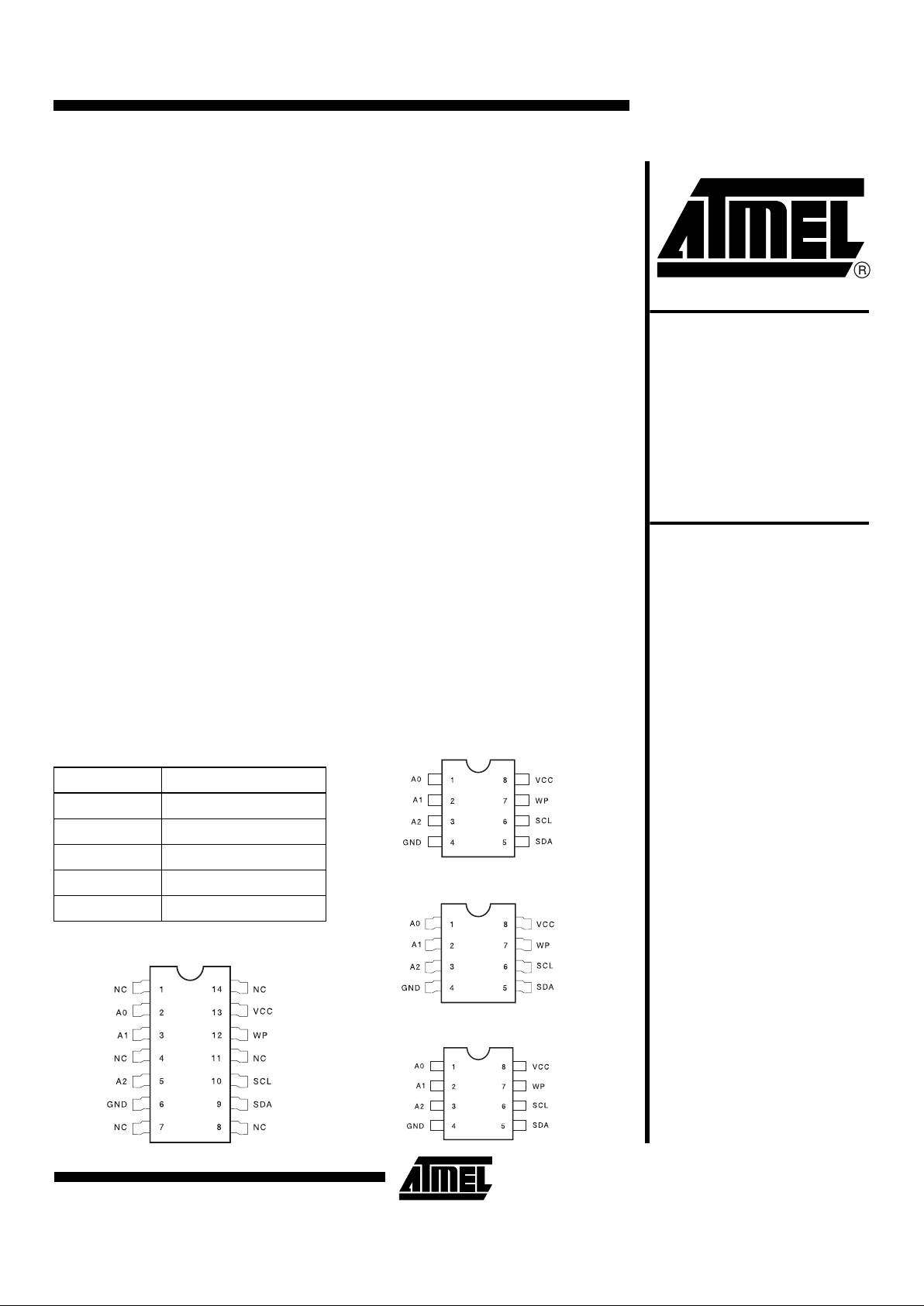
Pin Configurations
Pin Name Function
A
0
to A
2
Address Inputs
SDA Serial Data
SCL Serial Clock Input
WP Write Protect
NC No Connect
14-Pin SOIC
8-Pin PDIP
8-Pin SOIC
AT24C02A/04A/
08A
8-Pin TSSOP
AT24C02A/04A/08A
2
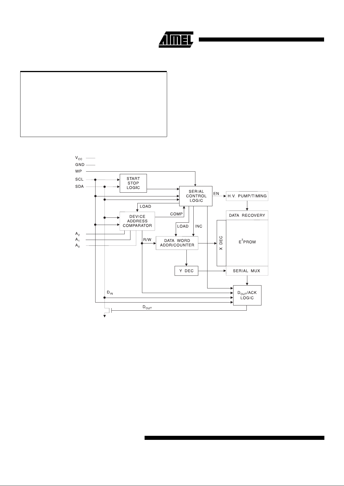
Block Diagram
Pin Description
SERIAL CLOCK (SCL):
The SCL input is used to positive
edge clock data into each EEPROM device and negative
edge clock data out of each device.
SERIAL DATA (SDA):
The SDA pin is bidirectional for
serial data transfer. This pin is open-drain driven and may
be wire-ORed with any number of other open-drain or open
collector devices.
DEVICE/PAGE ADDRESSES (A2 , A1, A0):
The A2, A1
and A0 pins are device address inputs that are hard wired
for the AT24C02A. As many as eight 2K devices may be
addressed on a single bus system (device address ing is
discussed in detail under the Device Addressing section).
The AT24C04A uses the A2 and A1 in puts for hard wir e
addressing and a total of four 4K devices may be
addressed on a singl e b us sy st em . The A0 pi n is a no c onnect.
The AT24C08A only uses the A2 input for hardwire
addressing and a total of two 8K devices may be
addressed on a single bus system. The A0 and A1 pins are
no connects.
WRITE PROTECT (WP):
The AT24C 02A/0 4A/08A has a
Write Protect pin that provides hardware data protection.
The Write Protect pin allows normal read/write operations
when connected to groun d (GND). Wh en the Write Pr otect
Absolute Maximum Ratings*
Operating Temperature.................................. -55°C to +125°C
*NOTICE: Stresses beyond those listed under “Absolute
Maximum Ratings” may cause permanent damage to the dev ice. Th is is a s tress rating only an d
functional oper ati on of the devi ce at t hes e o r any
other conditions beyond those indicated in the
operational sections of this specification is not
implied. Exposure to absolute maximum rating
conditions f or e xtended periods ma y af fect dev ice
reliability .
Storage Temperature..................................... -65°C to +150°C
Voltage on Any Pin
with Respect to Ground.....................................-1.0V to +7.0V
Maximum Operating Voltage........................................... 6.25V
DC Output Current........................................................5.0 mA
AT24C02A/04A/08A
3
pin is connec ted to V
CC
, the write protection feature is
enabled and operates as shown in the following table.
Memory Organization
AT24C02A, 2K SERIAL EEPROM:
Internally organized
with 256 pages of 1-byte each, the 2K requires an 8 bit
data word address for random word addressing.
AT24C04A, 4K SERIAL EEPROM:
The 4K is internally
organized with 256 pages of 2-bytes each. Rand om word
addressing requires a 9 bit data word address.
AT24C08A, 8K SERIAL EEPROM:
The 8K is internally
organized with 4 blocks of 256 pages of 4-bytes each.
Random word addressing requires a 10 bit data word
address.
Note: 1. This parameter is characterized and is not 100% tested.
Note: 1. V
IL
min and VIH max are reference only and are not tested.
WP Pin
Status
Part of the Array Protected
24C02A 24C04A 24C08A
At V
CC
Upper Half
(1K) Array
Upper Half
(2K) Array
Full (8K)
Array
At GND Normal Read/Write Operation s
Pin Capacitance
Applicable over recommended operating range from TA = 25°C, f = 1.0 MHz, VCC = +1.8V.
Symbol Test Condition Max Units Conditions
C
I/O
Input/Output Capacitance (SDA) 8 pF V
I/O
= 0V
C
IN
Input Capacitance (A0, A1, A2, SCL) 6 pF VIN = 0V
DC Characteristics
Applicable over recommended operating range from: TAI = -40°C to +85°C, VCC = +1.8V to +5.5V, TAC = 0°C to +70°C,
V
CC
= +1.8V to +5.5V (unless otherwise noted).
Symbol Parameter Test Condition Min Typ Max Units
V
CC1
Supply Voltage 1.8 5.5 V
V
CC2
Supply Voltage 2.5 5.5 V
V
CC3
Supply Voltage 2.7 5.5 V
V
CC4
Supply Voltage 4.5 5.5 V
I
CC
Supply Current VCC = 5.0V READ at 100 kHz 0.4 1.0 mA
I
CC
Supply Current VCC = 5.0V WRITE at 100 kHz 2.0 3.0 mA
I
SB1
Standby Current VCC = 1.8V VIN = VCC or V
SS
0.6 3.0
µ
A
I
SB2
Standby Current VCC = 2.5V VIN = VCC or V
SS
1.4 4.0
µ
A
I
SB3
Standby Current VCC = 2.7V VIN = VCC or V
SS
1.6 4.0
µ
A
I
SB4
Standby Current VCC = 5.0V VIN = VCC or V
SS
8.0 18.0
µ
A
I
LI
Input Leakage Current VIN = VCC or V
SS
0.10 3.0
µ
A
I
LO
Output Leakage Current V
OUT
= V
CC
or V
SS
0.05 3.0
µ
A
V
IL
Input Low Level
(1)
-0.6 VCC x 0.3 V
V
IH
Input High Level
(1)
VCC x 0.7 VCC + 0.5 V
V
OL2
Output Low Level VCC = 3.0V IOL = 2.1 mA 0.4 V
V
OL1
Output Low Level VCC = 1.8V IOL = 0.15 mA 0.2 V

AT24C02A/04A/08A
4
Note: 1. This parameter is characterized and is not 100% tested.
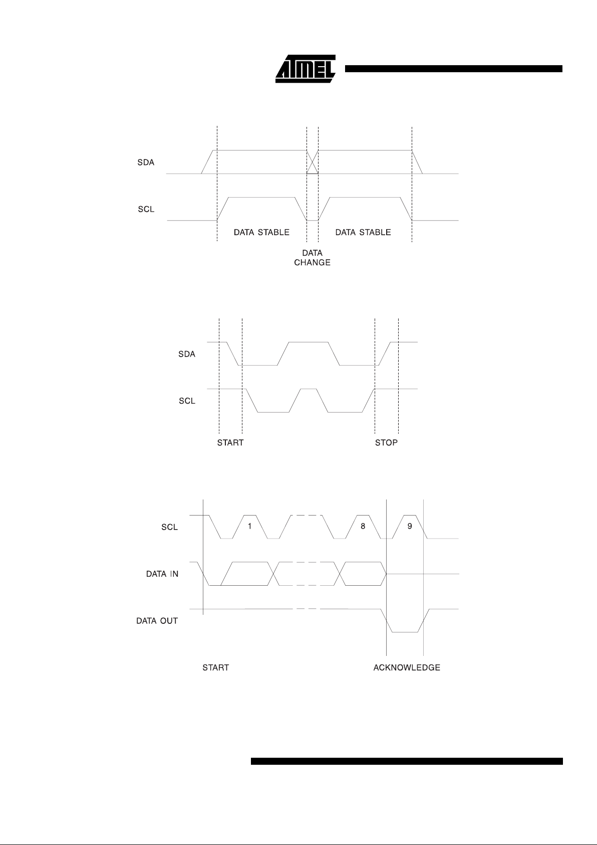
Device Operation
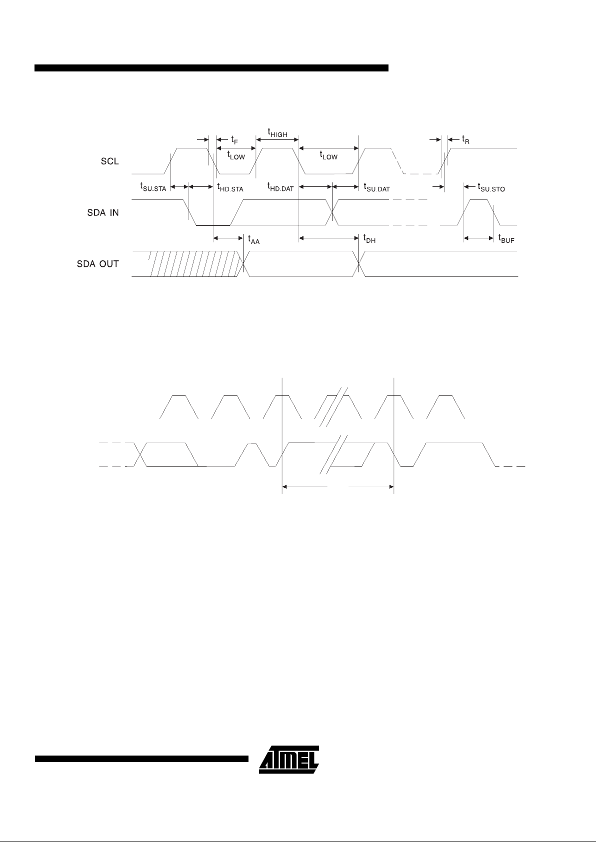
CLOCK and DATA TRANSITIONS:
The SDA pin is normally pulled high wi th an ex terna l dev ic e. Dat a o n t he SDA
pin may chan ge o nly d uri ng S CL l ow t ime per iods (refe r t o
Data Validity timing diagram). Data changes during S CL
high periods will indicate a start or stop condition as
defined below.
START CONDITION:
A high-to-low transition of SDA with
SCL high is a start condition which must precede any other
command (refer to Start and Stop Definition timing diagram).
STOP CONDITION:
A low-to-high transition of SDA with
SCL high is a stop condition. After a read sequence, the
stop command will place the EEPR OM in a standb y power
mode (refer to Start and Stop Definition timing diagram).
ACKNOWLEDGE:
All address es an d data words a re se ri-
ally transmitted to and from the EEPROM in 8 bit words
.
The EEPROM sends a ze ro to acknowledge that it has
received each word. This happens during the ninth clock
cycle.
STANDBY MODE:
The AT24C02A/04A/08A features a low
power standby mode which is enabled: (a) upon power-up
and (b) after the receipt of the STOP bit and the completion
of any internal operations.
MEMORY RESET:
After an interruption in protocol, power
loss or system reset, any 2-wire part can be reset by following these steps:(a ) Clock up to 9 cycle s, (b) look for SDA
high in each cycle while SCL is high and then (c) create a
start condition as SDA is high.
AC Characteristics
Applicable over recommended operating range from TA = -40°C to +85°C, VCC = +1.8V to +5.5V, CL = 1 TTL Gate and
100 pF (unless otherwise noted).
Symbol Parameter
2.7-, 2.5-, 1.8-volt 5.0-volt
UnitsMinMaxMinMax
f
SCL
Clock Frequency, SCL 100 400 kHz
t
LOW
Clock Pulse Width Low 4.7 1.2
µ
s
t
HIGH
Clock Pulse Width High 4.0 0.6
µ
s
t
I
Noise Suppression Time
(1)
100 50 ns
t
AA
Clock Low to Data Out Valid 0.1 4.5 0.1 0.9
µ
s
t
BUF
Time the bus must be free before
a new transmission can start
(1)
4.7 1.2
µ
s
t
HD.STA
Start Hold Time 4.0 0.6
µ
s
t
SU.STA
Start Set-up Time 4.7 0.6
µ
s
t
HD.DAT
Data In Hold Time 0 0
µ
s
t
SU.DAT
Data In Set-up Time 200 100 ns
t
R
Inputs Rise Time
(1)
1.0 0.3
µ
s
t
F
Inputs Fall Time
(1)
300 300 ns
t
SU.STO
Stop Set-up Time 4.7 0.6
µ
s
t
DH
Data Out Hold Time 100 50 ns
t
WR
Write Cycle Time 10 10 ms
Endurance
(1)
5.0V, 25°C, Page Mode 1M 1M
Write
Cycles
AT24C02A/04A/08A
5
Bus Timing (SCL: Serial Clock, SDA: Serial Data I/O)
Write Cycle Timing (SCL: Serial Clock, SDA: Serial Data I/O)
Note: 1. The write cycle time tWR is the time from a valid stop condition of a write sequence to the end of the interval
clear/write cycle.
SCL
SDA 8th BIT
WORD n
ACK
STOP
CONDITION
START
CONDITION
t
WR
(1)
AT24C02A/04A/08A
6
Data Validity
Start and Stop Definition
Output Acknowledge

AT24C02A/04A/08A
7
Device Addressing
The 2K, 4K and 8K EEPROM devices all require an 8 bit
device address word following a start condition to enable
the chip for a read or write operation (refer to Figure 1).
The device address word consists of a mandatory one,
zero sequence for th e first four most signifi cant bits as
shown. This is common to all the EEPROM devices.
The next 3 bits are the A2, A1 and A0 device address bits
for the 2K EEPROM. These 3 bits must compare to their
corresponding hard-wired input pins.
The 4K EEPROM onl y us es th e A 2 and A 1 d ev ic e add ress
bits with the third bit being a memory page address bit. The
two device address bi ts mus t compa re to the ir corr esponding hard-wired input pins. The A0 pin is no connect.
The 8K EEPROM only us es the A 2 devi ce add ress bi t with
the next 2 b its b eing for me mor y page add res sing. The A2
bit must compare to its c or re spon din g h ard- wir ed in put pin .
The A1 and A0 pins are no connect.
The eighth bit of the device address is the read/write operation select bit. A read operation is initiated if this bit is high
and a write operation is initiated if this bit is low.
Upon a compare of the device address, the EEPROM will
output a zero. If a compare is not m ade , the chi p wi ll r et urn
to a standby state.
Write Operations
BYTE WRITE:
A write operation requ ires an 8 bit data
word address following the device address word and
acknowledgement. Upon receipt of this a ddress, the
EEPROM will again respond with a zero and then clock in
the first 8 bit data word. Following receipt of the 8 bit data
word, the EEPROM will output a zero and the addr essing
device, such as a m icr oc ontr olle r, mu st term in ate the w rit e
sequence with a stop condition. At this time the
EEPROM
enters an internally-timed write cycle , t
WR
, to the nonvolatile memory. All inputs are disabled during this wr ite cycle
and the EEPROM will not respond until the write is complete (refer to Figure 2).
PAGE WRITE:
The 2K EEPROM is capable of an 8-byte
page write, and the 4K and 8K devices are capable of 16byte page writes.
A page write i s initi ated the same as a byte wri te, but the
microcontroller does not send a stop condition after the first
data word is clocked in. Instead, after the EEPROM
acknowledges receipt of the first data word, the microcontroller can transmit up to seven (2K) or fifteen (4K, 8K)
more data words. The EEPROM will respond with a zero
after each data word received. The mi crocontroller must
terminate the page write sequ ence with a stop cond ition
(refer to Figure 3).
The data word address lower three (2K) or four (4K, 8K)
bits are internally in cr em ente d fo ll owi ng the receipt of each
data word. The higher data word address bits are not incremented, retaining the memory page row location. When the
word address, internally generated, reaches the pa ge
boundary, the following byte is pl aced at the beginning of
the same page. If more than ei ght (2 K) or sixt een (4K , 8K)
data words are t ransmi tted to the EEPROM , the dat a word
address will “roll over ” and previous dat a will be overwritten.
ACKNOWLEDGE POLLING:
Once the internally-timed
write cycle has started and the EEPROM inpu ts are disabled, acknowledge polling can be initiated. T his invol ves
sending a start condition followed by the device address
word. The read/write bit is representati ve of the operati on
desired. Only if the internal wri te cycle has c ompleted will
the EEPROM respon d with a zero allowing the read or
write sequence to continue.
Read Operations
Read operations are initiated the same way as write operations with the exception that the read/write select bit in the
device address word is set to one. There are t hree read
operations: current address read, random address read
and sequential read.
CURRENT ADDRESS REA D:
The internal data word
address counter maintains the last address accessed during the last read or write operation, incremented by one.
This address stays valid between operations as long as the
chip power is maintained. T he address “roll ov er” during
read is from the last byte of the last memory page to the
first byte of the first page. The address “roll over” during
write is from the las t byte of the cur rent page to the first
byte of the same page.
Once the device address with the read/write select b it set
to one is clocked in and acknowledged by the EEPROM,
the current address data word is s erially clo cked out. The
microcontroller does not respond with an input zero but
does generate a following stop condition (refer to Figure 4).
RANDOM READ:
A random read require s a “dummy ” byte
write sequence to load in t he data wo rd addr ess. Once th e
device address word and data word address are clocked in
and acknowledged by the EE PROM, the mi crocontroll er
must generate another start condition. The microcontroller
now initiates a current address read by sending a device
address with the read/write select b it high. The EEP ROM
acknowledges the device address and serially clocks out
the data word. The microcontroller does not respond with a
zero but does generate a following stop condition (refer to
Figure 5).
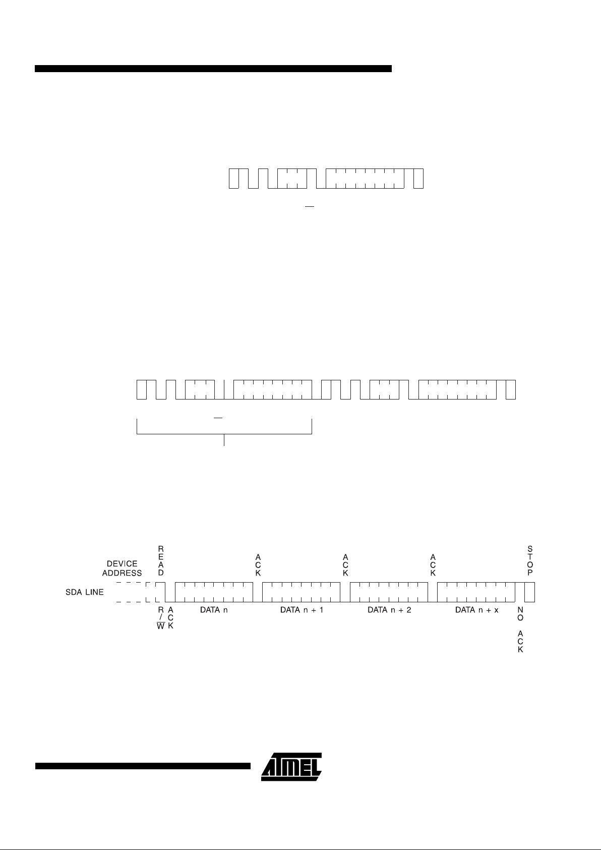
SEQUENTIAL READ:
Sequential reads are initiated by
either a current address read or a random address read.
After the microcontroller receives a data word, it responds

AT24C02A/04A/08A
8
with an acknowledge. As long as the EEPROM receives an
acknowledge, it will continue to increment the data word
address and serially clock out sequential data words. When
the memory address limit is reached, the data word
address will “roll over” and the sequential read will continue. The sequential read operation is terminated when
the microcontroller does not respond with a zero but does
generate a following stop condition (refer to Figure 6).
Figure 1.
Device Address
Figure 2.
Byte Write
Figure 3.
Page write
MSD
2K
LSB
1
A
2
A
0
A
1
R/W
4K
1
A
2
P0
A
1
R/W
0
0
0
0
0
0
1
1
18K 1
A
2
P0
P
1
R/W
S
T
A
R
T
M
S
B
M
S
B
L
S
B
S
T
O
P
W
R
I
T
E
SDA LINE
DEVICE
ADDRESS
WORD ADDRESS
DATA
L
S
B
A
C
K
A
C
K
A
C
K
R
/
W
S
T
A
R
T
M
S
B
S
T
O
P
W
R
I
T
E
SDA LINE
DEVICE
ADDRESS
WORD ADDRESS (n) DATA (n) DATA (n + 1) DATA (n + x)
L
S
B
A
C
K
A
C
K
A
C
K
A
C
K
A
C
K
R
/
W
AT24C02A/04A/08A
9
Figure 4.
Current Address Read
Figure 5.
Random Read
Figure 6.
Sequential Read
S
T
A
R
T
R
E
A
D
M
S
B
S
T
O
P
SDA LINE
DEVICE
ADDRESS
DATA
L
S
B
A
C
K
N
O
A
C
K
R
/
W
S
T
A
R
T
S
T
A
R
T
M
S
B
S
T
O
P
W
R
I
T
E
R
E
A
D
SDA LINE
DEVICE
ADDRESS
DUMMY WRITE
WORD
ADDRESS n
DEVICE
ADDRESS
DATA n
L
S
B
A
C
K
A
C
K
A
C
K
N
O
A
C
K
R
/
W
M
S
B
L
S
B
M
S
B
L
S
B

AT24C02A/04A/08A
10
AT24C02A Ordering Information
tWR (max)
(ms)
ICC (max)
(µµµµA)
ISB (max)
(µµµµA)
f
MAX
(kHz) Ordering Code Package Operation Range
10 3000 18 400 AT24C02A-10PC
AT24C02AN-10SC
AT24C02A-10SC
AT24C02A-10TC
8P3
8S1
14S
8T
Commercial
(0°C to 70°C)
3000 18 400 AT24C02A-10PI
AT24C02AN-10SI
AT24C02A-10SI
AT24C02A-10TI
8P3
8S1
14S
8T
Industrial
(-40°C to 85°C)
10 1500 4 100 AT24C02A-10PC-2.7
AT24C02AN-10SC-2.7
AT24C02A-10SC-2.7
AT24C02A-10TC-2.7
8P3
8S1
14S
8T
Commercial
(0°C to 70°C)
1500 4 100 AT24C02A-10PI-2.7
AT24C02AN-10SI-2.7
AT24C02A-10SI-2.7
AT24C02A-10TI-2.7
8P3
8S1
14S
8T
Industrial
(-40°C to 85°C)
10 1000 4 100 AT24C02A-10PC-2.5
AT24C02AN-10SC-2.5
AT24C02A-10SC-2.5
AT24C02A-10TC-2.5
8P3
8S1
14S
8T
Commercial
(0°C to 70°C)
1000 4 100 AT24C02A-10PI-2.5
AT24C02AN-10SI-2.5
AT24C02A-10SI-2.5
AT24C02A-10TI-2.5
8P3
8S1
14S
8T
Industrial
(-40°C to 85°C)
10 800 3 100 AT24C02A-10PC-1.8
AT24C02AN-10SC-1.8
AT24C02A-10SC-1.8
AT24C02A-10TC-1.8
8P3
8S1
14S
8T
Commercial
(0°C to 70°C)
800 3 100 AT24C02A-10PI-1.8
AT24C02AN-10SI-1.8
AT24C02A-10SI-1.8
AT24C02A-10TI-1.8
8P3
8S1
14S
8T
Industrial
(-40°C to 85°C)
Package Type
8P3 8-Lead, 0.300" Wide, Plastic Dual Inline Package (PDIP)
8S1 8-Lead, 0.150" Wide, Plastic Gull Wing Small Outline (JEDEC SOIC)
14S 14-Lead, 0.150" Wide, Plastic Gull Wing Small Outline (SOIC)
8T 8-Lead, 0.170” Wide, Thin Shrink Small Outline Package (TSSOP)
Options
Blank Standard Operation (4.5V to 5.5V)
-2.7 Low-Voltage (2.7V to 5.5V)
-2.5 Low-Voltage (2.5V to 5.5V)
-1.8 Low-Voltage (1.8V to 5.5V)

AT24C02A/04A/08A
11
AT24C04A Ordering Information
tWR (max)
(ms)
ICC (max)
(µµµµA)
ISB (max)
(µµµµA)
f
MAX
(kHz) Ordering Code Package Operation Range
10 3000 18 400 AT24C04A-10PC
AT24C04AN-10SC
AT24C04A-10SC
AT24C04A-10TC
8P3
8S1
14S
8T
Commercial
(0°C to 70°C)
3000 18 400 AT24C04A-10PI
AT24C04AN-10SI
AT24C04A-10SI
AT24C04A-10TI
8P3
8S1
14S
8T
Industrial
(-40°C to 85°C)
10 1500 4 100 AT24C04A-10PC-2.7
AT24C04AN-10SC-2.7
AT24C04A-10SC-2.7
AT24C04A-10TC
8P3
8S1
14S
8T
Commercial
(0°C to 70°C)
1500 4 100 AT24C04A-10PI-2.7
AT24C04AN-10SI-2.7
AT24C04A-10SI-2.7
AT24C04A-10TI-2.7
8P3
8S1
14S
8T
Industrial
(-40°C to 85°C)
10 1000 4 100 AT24C04A-10PC-2.5
AT24C04AN-10SC-2.5
AT24C04A-10SC-2.5
AT24C04A-10TC-2.5
8P3
8S1
14S
8T
Commercial
(0°C to 70°C)
1000 4 100 AT24C04A-10PI-2.5
AT24C04AN-10SI-2.5
AT24C04A-10SI-2.5
AT24C04A-10TI-2.5
8P3
8S1
14S
8T
Industrial
(-40°C to 85°C)
10 800 3 100 AT24C04A-10PC-1.8
AT24C04AN-10SC-1.8
AT24C04A-10SC-1.8
AT24C04A-10TC-1.8
8P3
8S1
14S
8T
Commercial
(0°C to 70°C)
800 3 100 AT24C04A-10PI-1.8
AT24C04AN-10SI-1.8
AT24C04A-10SI-1.8
AT24C04A-10TI-1.8
8P3
8S1
14S
8T
Industrial
(-40°C to 85°C)
Package Type
8P3 8-Lead, 0.300" Wide, Plastic Dual Inline Package (PDIP)
8S1 8-Lead, 0.150" Wide, Plastic Gull Wing Small Outline (JEDEC SOIC)
14S 14-Lead, 0.150" Wide, Plastic Gull Wing Small Outline (SOIC)
8T 8-Lead, 0.170” Wide, Thin Shrink Small Outline Package (TSSOP)
Options
Blank Standard Operation (4.5V to 5.5V)
-2.7 Low-Voltage (2.7V to 5.5V)
-2.5 Low-Voltage (2.5V to 5.5V)
-1.8 Low-Voltage (1.8V to 5.5V)

AT24C02A/04A/08A
12
AT24C08A Ordering Information
tWR (max)
(ms)
ICC (max)
(µµµµA)
ISB (max)
(µµµµA)
f
MAX
(kHz) Ordering Code Package Operation Range
10 3000 18 400 AT24C08A-10PC
AT24C08AN-10SC
AT24C08A-10SC
AT24C08A-10TC
8P3
8S1
14S
8T
Commercial
(0°C to 70°C)
3000 18 400 AT24C08A-10PI
AT24C08AN-10SI
AT24C08A-10SI
AT24C08A-10TI
8P3
8S1
14S
8T
Industrial
(-40°C to 85°C)
10 1500 4 100 AT24C08A-10PC-2.7
AT24C08AN-10SC-2.7
AT24C08A-10SC-2.7
AT24C08A-10TC-2.7
8P3
8S1
14S
8T
Commercial
(0°C to 70°C)
1500 4 100 AT24C08A-10PI-2.7
AT24C08AN-10SI-2.7
AT24C08A-10SI-2.7
AT24C08A-10TI-2.7
8P3
8S1
14S
8T
Industrial
(-40°C to 85°C)
10 1000 4 100 AT24C08A-10PC-2.5
AT24C08AN-10SC-2.5
AT24C08A-10SC-2.5
AT24C08A-10TC-2.5
8P3
8S1
14S
8T
Commercial
(0°C to 70°C)
1000 4 100 AT24C08A-10PI-2.5
AT24C08AN-10SI-2.5
AT24C08A-10SI-2.5
AT24C08A-10TI-2.5
8P3
8S1
14S
8T
Industrial
(-40°C to 85°C)
10 800 3 100 AT24C08A-10PC-1.8
AT24C08AN-10SC-1.8
AT24C08A-10SC-1.8
AT24C08A-10TC-1.8
8P3
8S1
14S
8T
Commercial
(0°C to 70°C)
800 3 100 AT24C08A-10PI-1.8
AT24C08AN-10SI-1.8
AT24C08A-10SI-1.8
AT24C08A-10TI-1.8
8P3
8S1
14S
8T
Industrial
(-40°C to 85°C)
Package Type
8P3 8-Lead, 0.300" Wide, Plastic Dual Inline Package (PDIP)
8S1 8-Lead, 0.150" Wide, Plastic Gull Wing Small Outline (JEDEC SOIC)
14S 14-Lead, 0.150" Wide, Plastic Gull Wing Small Outline (SOIC)
8T 8-Lead, 0.170” Wide, Thin Shrink Small Outline Package (TSSOP)
Options
Blank Standard Operation (4.5V to 5.5V)
-2.7 Low-Voltage (2.7V to 5.5V)
-2.5 Low-Voltage (2.5V to 5.5V)
-1.8 Low-Voltage (1.8V to 5.5V)

AT24C02A/04A/08A
13
Packaging Information
.400 (10.16)
.355 (9.02)
PIN
1
.280 (7.11)
.240 (6.10)
.037 (.940)
.027 (.690)
.300 (7.62) REF
.210 (5.33) MAX
SEATING
PLANE
.100 (2.54) BSC
.015 (.380) MIN
.022 (.559)
.014 (.356)
.150 (3.81)
.115 (2.92)
.070 (1.78)
.045 (1.14)
.325 (8.26)
.300 (7.62)
0
15
REF
.430 (10.9) MAX
.012 (.305)
.008 (.203)
.020 (.508)
.013 (.330)
PIN 1
.157 (3.99)
.150 (3.81)
.244 (6.20)
.228 (5.79)
.050 (1.27) BSC
.196 (4.98)
.189 (4.80)
.068 (1.73)
.053 (1.35)
.010 (.254)
.004 (.102)
0
8
REF
.010 (.254)
.007 (.203)
.050 (1.27)
.016 (.406)
.020 (.508)
.013 (.330)
.158 (4.01)
.152 (3.86)
.344 (8.74)
.337 (8.56)
.068 (1.73)
.053 (1.35)
.010 (.249)
.004 (.102)
.010 (.249)
.008 (.191)
.050 (1.27)
.016 (.406)
.244 (6.20)
.228 (5.79)
.050 (1.27) BSC
0
8
REF
PIN 1
*Controlling dimension: millimeters
6.50 (.256)
6.25 (.246)
0.30 (.012)
0.19 (.008)
.65 (.026) BSC
1.05 (.041)
0.80 (.033)
3.10 (.122)
4.5 (.177)
2.90 (.114)
4.3 (.169)
0.15 (.006)
0.05 (.002)
1.20 (.047) MAX
0.20 (.008)
0.75 (.030)
0.09 (.004)
0.45 (.018)
0
8
REF
PIN 1
8P3
, 8-Lead, 0.300" Wide,
Plastic Dual Inline Package (PDIP)
Dimensions in Inches and (Millimeters)
JEDEC STANDARD MS-001 BA
8S1
, 8-Lead, 0.150" Wide,
Plastic Gull Wing Small Outline (JEDEC SOIC)
Dimensions in Inches and (Millimeters)
14S
, 14-Lead, 0.150" Wide,
Plastic Gull Wing Small Outline (SOIC)
Dimensions in Inches and (Millimeters)
8T,
8-Lead, 0.170” Wide, Plastic Thin Small Outline
Package (TSSOP)
Dimensions in Millimeters and (Inches)*
 Loading...