

Features
C
A
V
S
D
G
C
G
C
L
A
• Low-voltage and Standard-voltage Operation
– 2.7 (VCC = 2.7V to 5.5V)
– 1.8 (V
• Internally Organized 128 x 8 (1K), 256 x 8 (2K), 512 x 8 (4K),
1024 x 8 (8K) or 2048 x 8 (16K)
• Two-wire Serial Interface
• Schmitt Trigger, Filtered Inputs for Noise Suppression
• Bidirectional Data Transfer Protocol
• 100 kHz (1.8V) and 400 kHz (2.7V, 5V) Compatibility
• Write Protect Pin for Hardware Data Protection
• 8-byte Page (1K, 2K), 16-byte Page (4K, 8K, 16K) Write Modes
• Partial Page Writes Allowed
• Self-timed Write Cycle (5 ms max)
• High-reliability
– Endurance: 1 Million Write Cycles
– Data Retention: 100 Years
• Automotive Devices Available
• 8-lead JEDEC PDIP, 8-lead JEDEC SOIC, 8-lead Ultra Thin Mini-MAP (MLP 2x3), 5-lead
SOT23, 8-lead TSSOP and 8-ball dBGA2 Packages
• Die Sales: Wafer Form, Waffle Pack and Bumped Wafers
= 1.8V to 5.5V)
CC
Two-wire
Serial EEPROM
1K (128 x 8)
2K (256 x 8)
4K (512 x 8)
8K (1024 x 8)
Description
The AT24C01A/02/04/08A/16A provides 1024/2048/4096/8192/16384 bits of serial
electrically erasable and programmable read-only memory (EEPROM) organized as
128/256/512/1024/2048 words of 8 bits each. The device is optimized for use in many
industrial and commercial applications where low-power and low-voltage operation
are essential. The AT24C01A/02/04/08A/16A is available in space-saving 8-lead
PDIP, 8-lead JEDEC SOIC,
(AT24C01A/AT24C02/AT24C04), 8-lead TSSOP, and 8-ball dBGA2 packages and is
accessed via a Two-wire serial interface. In addition, the entire family is available in
2.7V (2.7V to 5.5V) and 1.8V (1.8V to 5.5V) versions.
Table 1. Pin Configuration
Pin Name Function
A0 - A2 Address Inputs
SDA Serial Data
SCL Serial Clock Input
WP Write Protect
NC No Connect
GND Ground
VCC Power Supply
8-lead Ultra Thin Mini-MAP (MLP 2x3), 5-lead SOT23
8-lead TSSOP
1
A0
2
A1
3
A2
4
ND
8-ball dBGA2
8
VCC
7
WP
6
SCL
5
SDA
8
VC
WP
7
SC
6
SD
5
GND
8-lead Ultra Thin Mini-MAP
1
A0
2
A1
3
A2
4
GND
A0
A1
A2
CC
WP
SCL
DA
8-lead SOIC
1
2
3
4
(MLP 2x3)
8
7
6
5
VCC
8
WP
7
SCL
6
SDA
5
A0
1
A1
2
A2
3
GN
4
Bottom View
8-lead PDIP
Bottom View
5-lead SOT23
8
VC
WP
7
SCL
6
SD
5
SCL
ND
SDA
1
2
3
WP
5
VC
4
GND
A0
A1
A2
1
2
3
4
16K (2048 x 8)
AT24C01A
AT24C02
(1)
(2)
AT24C04
AT24C08A
AT24C16A
Notes: 1. Not Recommended for
new design; Please
refer to AT24C01B
datasheet.
2. Not Recommended for
new design; Please
refer to AT24C02B
datasheet.
3. Not Recommended for
new design; Please
refer to AT24C16B
datasheet
(3)
0180Z1–SEEPR–5/07
1
Absolute Maximum Ratings
Operating Temperature..................................–55°C to +125°C
Storage Temperature .....................................–65°C to +150°C
Voltage on Any Pin
with Respect to Ground ....................................–1.0V to +7.0V
Maximum Operating Voltage .......................................... 6.25V
DC Output Current........................................................ 5.0 mA
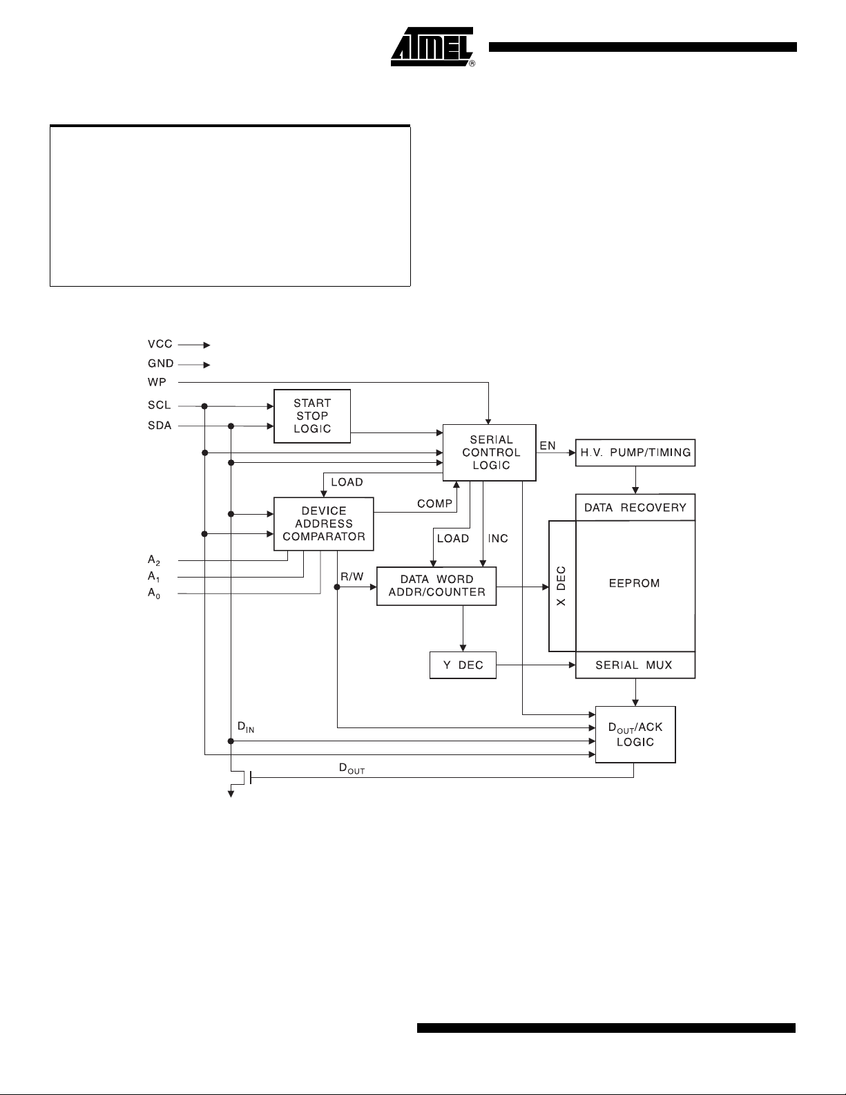
Figure 1. Block Diagram
*NOTICE: Stresses beyond those listed under “Absolute
Maximum Ratings” may cause permanent damage to the device. This is a stress rating only and
functional operation of the device at these or any
other conditions beyond those indicated in the
operational sections of this specification is not
implied. Exposure to absolute maximum rating
conditions for extended periods may affect
device reliability.
2
AT24C01A/02/04/08A/16A
0180Z1–SEEPR–5/07
AT24C01A/02/04/08A/16A
Pin Description SERIAL CLOCK (SCL): The SCL input is used to positive edge clock data into each
EEPROM device and negative edge clock data out of each device.
SERIAL DATA (SDA): The SDA pin is bidirectional for serial data transfer. This pin is
open-drain driven and may be wire-ORed with any number of other open-drain or opencollector devices.
DEVICE/PAGE ADDRESSES (A2, A1, A0): The A2, A1 and A0 pins are device
address inputs that are hard wired for the AT24C01A and the AT24C02. As many as
eight 1K/2K devices may be addressed on a single bus system (device addressing is
discussed in detail under the Device Addressing section).
The AT24C04 uses the A2 and A1 inputs for hard wire addressing and a total of four 4K
devices may be addressed on a single bus system. The A0 pin is a no connect and can
be connected to ground.
The AT24C08A only uses the A2 input for hardwire addressing and a total of two 8K
devices may be addressed on a single bus system. The A0 and A1 pins are no connects
and can be connected to ground.
The AT24C16A does not use the device address pins, which limits the number of
devices on a single bus to one. The A0, A1 and A2 pins are no connects and can be
connected to ground.
WRITE PROTECT (WP): The AT24C01A/02/04/08A/16A has a Write Protect pin that
provides hardware data protection. The Write Protect pin allows normal Read/Write
operations when connected to ground (GND). When the Write Protect pin is connected
to V
, the write protection feature is enabled and operates as shown in Table 2.
CC
Table 2. Write Protect
WP Pin
Status
At V
CC
At GND Normal Read/Write Operations
24C01A 24C02 24C04 24C08A 24C16A
Full (1K)
Array
Full (2K)
Array
Part of the Array Protected
Full (4K)
Array
Full (8K)
Array
Full (16K)
Array
Memory Organization AT24C01A, 1K SERIAL EEPROM: Internally organized with 16 pages of 8 bytes each,
the 1K requires a 7-bit data word address for random word addressing.
AT24C02, 2K SERIAL EEPROM: Internally organized with 32 pages of 8 bytes each,
the 2K requires an 8-bit data word address for random word addressing.
AT24C04, 4K SERIAL EEPROM: Internally organized with 32 pages of 16 bytes each,
the 4K requires a 9-bit data word address for random word addressing.
AT24C08A, 8K SERIAL EEPROM: Internally organized with 64 pages of 16 bytes
each, the 8K requires a 10-bit data word address for random word addressing.
0180Z1–SEEPR–5/07
AT24C16A, 16K SERIAL EEPROM: Internally organized with 128 pages of 16 bytes
each, the 16K requires an 11-bit data word address for random word addressing.
3
Table 3. Pin Capacitance
(1)
Applicable over recommended operating range from TA = 25°C, f = 1.0 MHz, VCC = +1.8V
Symbol Test Condition Max Units Conditions
C
I/O
C
IN
Input/Output Capacitance (SDA) 8 pF V
Input Capacitance (A0, A1, A2, SCL) 6 pF VIN = 0V
I/O
= 0V
Note: 1. This parameter is characterized and is not 100% tested.
Table 4. DC Characteristics
Applicable over recommended operating range from: T
= –40°C to +85°C, VCC = +1.8V to +5.5V, VCC= +1.8V to +5.5V
AI
(unless otherwise noted)
Symbol Parameter Test Condition Min Typ Max Units
V
CC1
V
CC2
V
CC3
I
CC
I
CC
I
SB1
I
SB2
I
SB3
I
SB4
I
LI
I
LO
V
IL
V
IH
V
OL2
V
OL1
Note: 1. V
Supply Voltage 1.8 5.5 V
Supply Voltage 2.7 5.5 V
Supply Voltage 4.5 5.5 V
Supply Current VCC = 5.0V READ at 100 kHz 0.4 1.0 mA
Supply Current VCC = 5.0V WRITE at 100 kHz 2.0 3.0 mA
Standby Current VCC = 1.8V VIN = VCC or V
Standby Current VCC = 2.5V VIN = VCC or V
Standby Current VCC = 2.7V VIN = VCC or V
Standby Current VCC = 5.0V VIN = VCC or V
Input Leakage Current VIN = VCC or V
Output Leakage Current V
Input Low Level
Input High Level
(1)
(1)
OUT
= V
CC
or V
SS
SS
SS
SS
SS
SS
–0.6 VCC x 0.3 V
VCC x 0.7 VCC + 0.5 V
0.6 3.0 µA
1.4 4.0 µA
1.6 4.0 µA
8.0 18.0 µA
0.10 3.0 µA
0.05 3.0 µA
Output Low Level VCC = 3.0V IOL = 2.1 mA 0.4 V
Output Low Level VCC = 1.8V IOL = 0.15 mA 0.2 V
min and V
IL
max are reference only and are not tested.
IH
4
AT24C01A/02/04/08A/16A
0180Z1–SEEPR–5/07
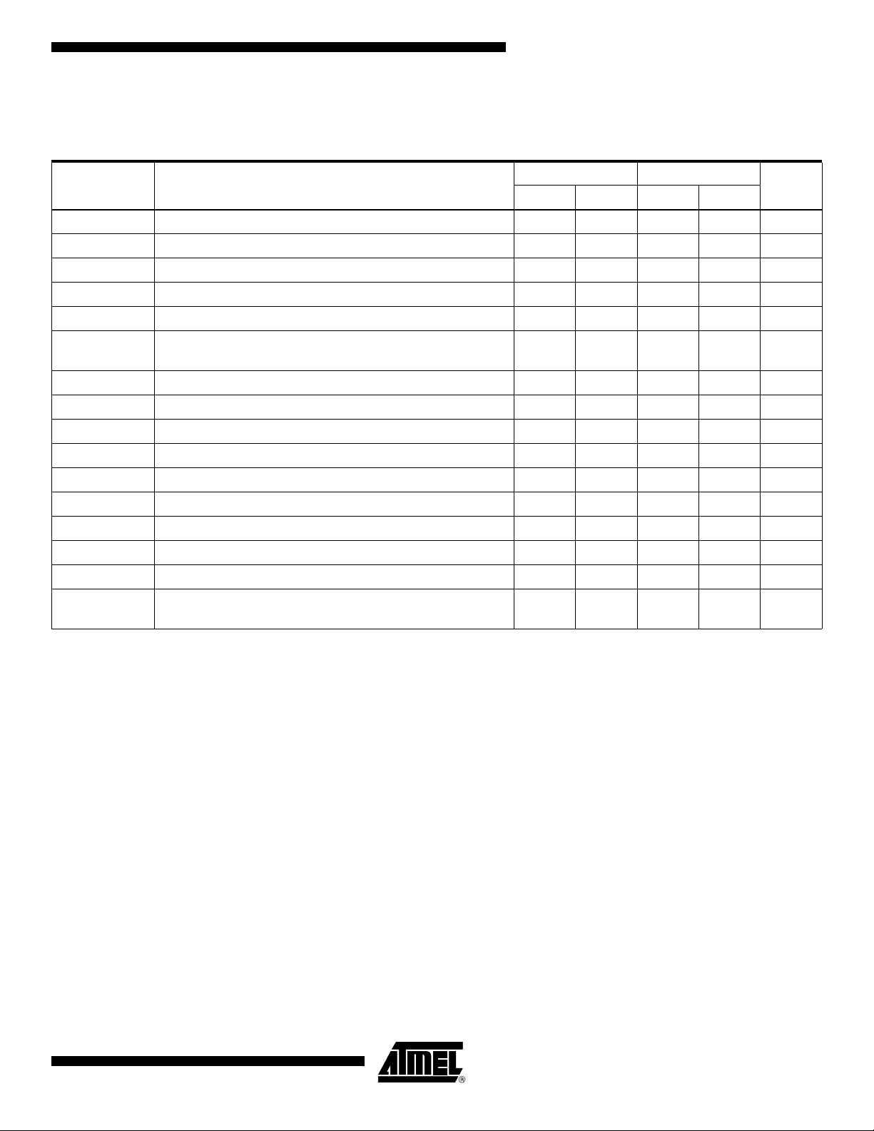
Table 5. AC Characteristics
Applicable over recommended operating range from T
CL = 1 TTL Gate and 100 pF (unless otherwise noted)
AT24C01A/02/04/08A/16A
= –40°C to +85°C, VCC = +1.8V to +5.5V, VCC = +2.7V to +5.5V,
AI
1.8-volt 2.7, 5.0-volt
Symbol Parameter
f
SCL
t
LOW
t
HIGH
t
I
t
AA
t
BUF
t
HD.STA
t
SU.STA
t
HD.DAT
t
SU.DAT
t
R
t
F
t
SU.STO
t
DH
t
WR
Endurance
Clock Frequency, SCL 100 400 kHz
Clock Pulse Width Low 4.7 1.2 µs
Clock Pulse Width High 4.0 0.6 µs
Noise Suppression Time
Clock Low to Data Out Valid 0.1 4.5 0.1 0.9 µs
Time the bus must be free before
a new transmission can start
Start Hold Time 4.0 0.6 µs
Start Setup Time 4.7 0.6 µs
Data In Hold Time 0 0 µs
Data In Setup Time 200 100 ns
Inputs Rise Time
Inputs Fall Time
(1)
(1)
Stop Setup Time 4.7 0.6 µs
Data Out Hold Time 100 50 ns
Write Cycle Time 5 5 ms
(1)
5.0V, 25°C, Byte Mode 1M 1M
Note: 1. This parameter is characterized.
UnitsMin Max Min Max
(1)
(1)
4.7 1.2 µs
100 50 ns
1.0 0.3 µs
300 300 ns
Write
Cycles
0180Z1–SEEPR–5/07
5

Device Operation CLOCK and DATA TRANSITIONS: The SDA pin is normally pulled high with an exter-
nal device. Data on the SDA pin may change only during SCL low time periods (see
Figure 4 on page 7). Data changes during SCL high periods will indicate a start or stop
condition as defined below.
START CONDITION: A high-to-low transition of SDA with SCL high is a start condition
which must precede any other command (see Figure 5 on page 8).
STOP CONDITION: A low-to-high transition of SDA with SCL high is a stop condition.
After a read sequence, the stop command will place the EEPROM in a standby power
mode (see Figure 5 on page 8).
ACKNOWLEDGE: All addresses and data words are serially transmitted to and from
the EEPROM in 8-bit words. The EEPROM sends a zero to acknowledge that it has
received each word. This happens during the ninth clock cycle.
STANDBY MODE: The AT24C01A/02/04/08A/16A features a low-power standby mode
which is enabled: (a) upon power-up and (b) after the receipt of the STOP bit and the
completion of any internal operations.
MEMORY RESET: After an interruption in protocol, power loss or system reset, any 2wire part can be reset by following these steps:
1. Clock up to 9 cycles.
2. Look for SDA high in each cycle while SCL is high.
3. Create a start condition.
6
AT24C01A/02/04/08A/16A
0180Z1–SEEPR–5/07
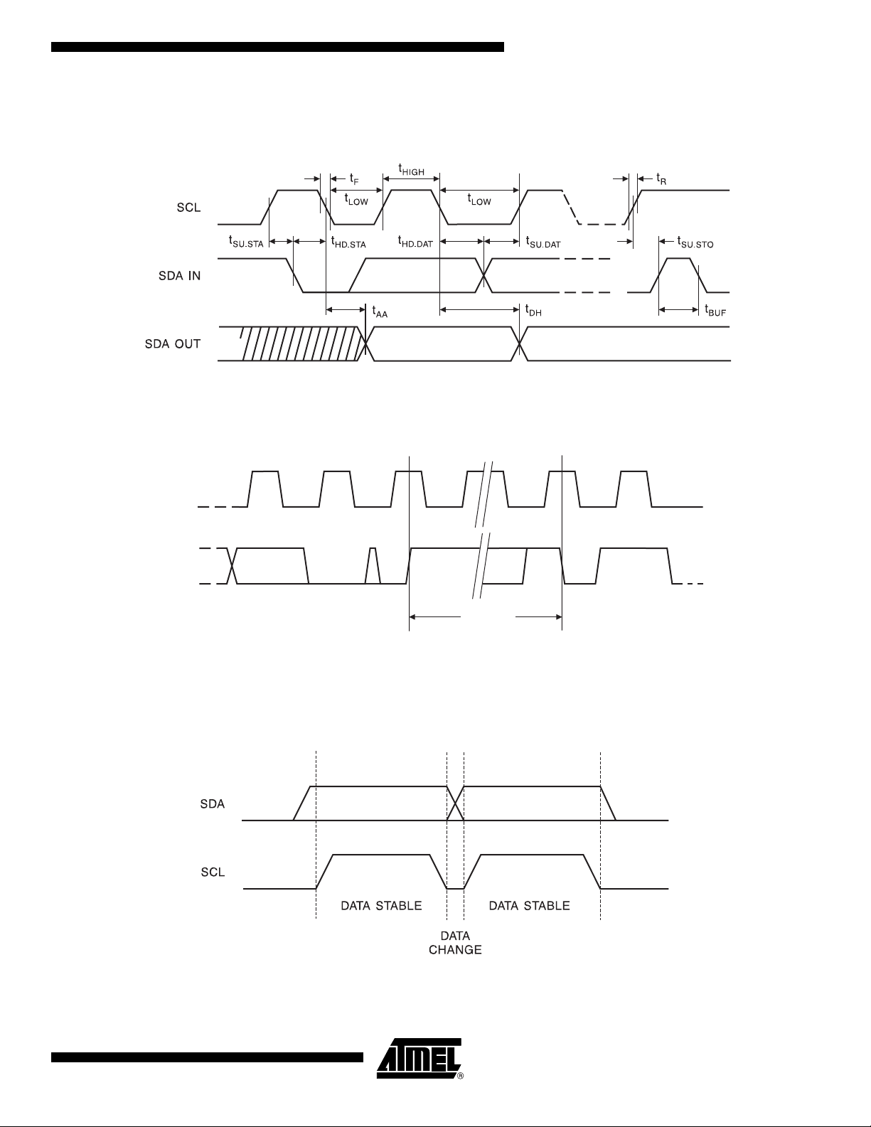
Bus Timing
S
S
Figure 2. SCL: Serial Clock, SDA: Serial Data I/O®
Write Cycle Timing
Figure 3. SCL: Serial Clock, SDA: Serial Data I/O
AT24C01A/02/04/08A/16A
CL
DA
Note: 1. The write cycle time tWR is the time from a valid stop condition of a write sequence to the end of the internal clear/write cycle.
8th BIT
WORDn
ACK
STOP
CONDITION
(1)
t
wr
START
CONDITION
Figure 4. Data Validity
7
0180Z1–SEEPR–5/07
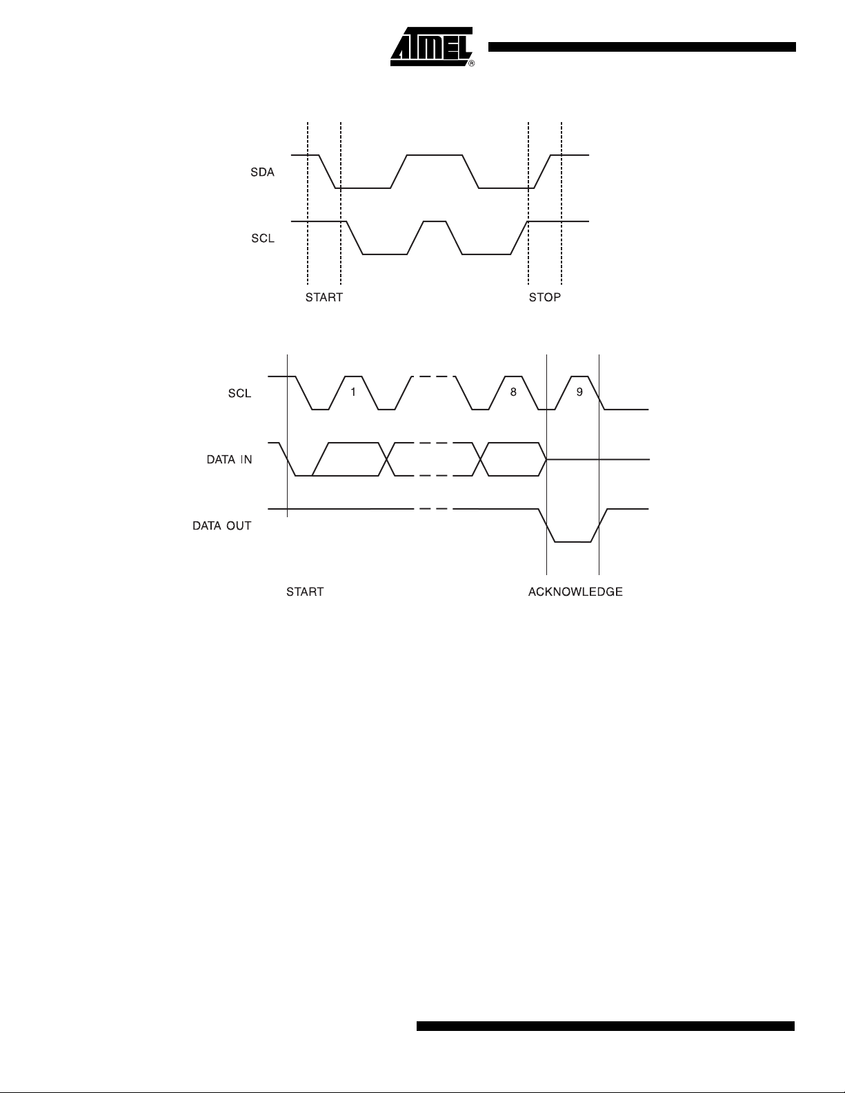
Figure 5. Start and Stop Definition
Figure 6. Output Acknowledge
8
AT24C01A/02/04/08A/16A
0180Z1–SEEPR–5/07

AT24C01A/02/04/08A/16A
Device Addressing The 1K, 2K, 4K, 8K and 16K EEPROM devices all require an 8-bit device address word
following a start condition to enable the chip for a read or write operation (refer to Figure
7).
The device address word consists of a mandatory one, zero sequence for the first four
most significant bits as shown. This is common to all the EEPROM devices.
The next 3 bits are the A2, A1 and A0 device address bits for the 1K/2K EEPROM.
These 3 bits must compare to their corresponding hard-wired input pins.
The 4K EEPROM only uses the A2 and A1 device address bits with the third bit being a
memory page address bit. The two device address bits must compare to their corresponding hard-wired input pins. The A0 pin is no connect.
The 8K EEPROM only uses the A2 device address bit with the next 2 bits being for
memory page addressing. The A2 bit must compare to its corresponding hard-wired
input pin. The A1 and A0 pins are no connect.
The 16K does not use any device address bits but instead the 3 bits are used for memory page addressing. These page addressing bits on the 4K, 8K and 16K devices
should be considered the most significant bits of the data word address which follows.
The A0, A1 and A2 pins are no connect.
The eighth bit of the device address is the read/write operation select bit. A read operation is initiated if this bit is high and a write operation is initiated if this bit is low.
Upon a compare of the device address, the EEPROM will output a zero. If a compare is
not made, the chip will return to a standby state.
Write Operations BYTE WRITE: A write operation requires an 8-bit data word address following the
device address word and acknowledgment. Upon receipt of this address, the EEPROM
will again respond with a zero and then clock in the first 8-bit data word. Following
receipt of the 8-bit data word, the EEPROM will output a zero and the addressing
device, such as a microcontroller, must terminate the write sequence with a stop condition. At this time the EEPROM enters an internally timed write cycle, t
nonvolatile memory. All inputs are disabled during this write cycle and the EEPROM will
not respond until the write is complete (see Figure 8 on page 11).
PAGE WRITE: The 1K/2K EEPROM is capable of an 8-byte page write, and the 4K, 8K
and 16K devices are capable of 16-byte page writes.
A page write is initiated the same as a byte write, but the microcontroller does not send
a stop condition after the first data word is clocked in. Instead, after the EEPROM
acknowledges receipt of the first data word, the microcontroller can transmit up to seven
(1K/2K) or fifteen (4K, 8K, 16K) more data words. The EEPROM will respond with a zero
after each data word received. The microcontroller must terminate the page write
sequence with a stop condition (see Figure 9 on page 11).
The data word address lower three (1K/2K) or four (4K, 8K, 16K) bits are internally
incremented following the receipt of each data word. The higher data word address bits
are not incremented, retaining the memory page row location. When the word address,
internally generated, reaches the page boundary, the following byte is placed at the
beginning of the same page. If more than eight (1K/2K) or sixteen (4K, 8K, 16K) data
words are transmitted to the EEPROM, the data word address will “roll over” and previous data will be overwritten.
, to the
WR
0180Z1–SEEPR–5/07
9

ACKNOWLEDGE POLLING: Once the internally timed write cycle has started and the
EEPROM inputs are disabled, acknowledge polling can be initiated. This involves sending a
start condition followed by the device address word. The read/write bit is representative of the
operation desired. Only if the internal write cycle has completed will the EEPROM respond
with a zero allowing the read or write sequence to continue.
Read Operations
Read operations are initiated the same way as write operations with the exception that the
read/write select bit in the device address word is set to one. There are three read operations:
current address read, random address read and sequential read.
CURRENT ADDRESS READ: The internal data word address counter maintains the last
address accessed during the last read or write operation, incremented by one. This address
stays valid between operations as long as the chip power is maintained. The address “roll
over” during read is from the last byte of the last memory page to the first byte of the first page.
The address “roll over” during write is from the last byte of the current page to the first byte of
the same page.
Once the device address with the read/write select bit set to one is clocked in and acknowledged by the EEPROM, the current address data word is serially clocked out. The
microcontroller does not respond with an input zero but does generate a following stop condition (see Figure 10 on page 12).
RANDOM READ: A random read requires a “dummy” byte write sequence to load in the data
word address. Once the device address word and data word address are clocked in and
acknowledged by the EEPROM, the microcontroller must generate another start condition.
The microcontroller now initiates a current address read by sending a device address with the
read/write select bit high. The EEPROM acknowledges the device address and serially clocks
out the data word. The microcontroller does not respond with a zero but does generate a following stop condition (see Figure 11 on page 12).
SEQUENTIAL READ: Sequential reads are initiated by either a current address read or a random address read. After the microcontroller receives a data word, it responds with an
acknowledge. As long as the EEPROM receives an acknowledge, it will continue to increment
the data word address and serially clock out sequential data words. When the memory
address limit is reached, the data word address will “roll over” and the sequential read will continue. The sequential read operation is terminated when the microcontroller does not respond
with a zero but does generate a following stop condition (see Figure 12 on page 12).
10
AT24C01A/02/04/08A/16A
0180Z1–SEEPR–5/07

Figure 7. Device Address
Figure 8. Byte Write
AT24C01A/02/04/08A/16A
MSB
8K
16K
Figure 9. Page Write
(* = DON’T CARE bit for 1K)
0180Z1–SEEPR–5/07
11

Figure 10. Current Address Read
Figure 11. Random Read
(* = DON’T CARE bit for 1K)
Figure 12. Sequential Read
12
AT24C01A/02/04/08A/16A
0180Z1–SEEPR–5/07
AT24C01A/02/04/08A/16A
AT24C01A Ordering Information
(1)
Ordering Code Package Operation Range
AT24C01A-10PU-2.7
AT24C01A-10PU-1.8
AT24C01A-10SU-2.7
AT24C01A-10SU-1.8
AT24C01A-10TU-2.7
AT24C01A-10TU-1.8
(2)
(2)
(2)
(2)
(2)
(2)
AT24C01A-10TSU-1.8
AT24C01AU3-10UU-1.8
AT24C01AY1-10YU-1.8
design)
AT24C01AY6-10YH-1.8
AT24C01A-W1.8-11
(4)
(2)
(2)
(2)
(Not recommended for new
(3)
8P3
8P3
8S1
8S1
8A2
8A2
5TS1
Lead-free/Halogen-free/
Industrial Temperature
(–40°C to 85°C)
8U31
8Y1
8Y6
Die Sale Industrial Temperature
(–40°C to 85°C)
Notes: 1. This device is not recommended for new design. Please refer to AT24C01B datasheet. For 2.7V devices used in the 4.5V to
5.5V range, please refer to performance values in the AC and DC characteristics table.
2. “U” designates Green Package + RoHS compliant.
3. “H” designates Green Package + RoHS compliant, with NiPdAu Lead Finish.
4. Available in waffle pack and wafer form; order as SL788 for inkless wafer form. Bumped die available upon request. Please
contact Serial EEPROM Marketing.
Package Type
8P3 8-lead, 0.300" Wide, Plastic Dual Inline Package (PDIP)
8S1 8-lead, 0.150" Wide, Plastic Gull Wing Small Outline (JEDEC SOIC)
8A2 8-lead, 4.4 mm Body, Plastic Thin Shrink Small Outline Package (TSSOP)
8Y1 8-lead, 4.90 mm x 3.00 mm Body, Dual Footprint, Non-leaded, Miniature Array Package (MAP)
8Y6 8-lead, 2.00 x 3.00 mm Body, 0.50 mm Pitch, Ultra Thin Mini-MAP, Dual No Lead Package (DFN), (MLP 2x3 mm)
5TS1 5-lead, 2.90 mm x 1.60 mm Body, Plastic Thin Shrink Small Outline Package (SOT23)
8U3-1 8-ball, die Ball Grid Away Package (dBGA2)
Options
–2.7 Low-voltage (2.7V to 5.5V)
–1.8 Low-voltage (1.8V to 5.5V)
0180Z1–SEEPR–5/07
13
AT24C02 Ordering Information
(1)
Ordering Code Package Operation Range
AT24C02-10PU-2.7
AT24C02-10PU-1.8
(2)
(2)
AT24C02N-10SU-2.7
AT24C02N-10SU-1.8
AT24C02-10TU-2.7
AT24C02-10TU-1.8
(2)
(2)
AT24C02Y1-10YU-1.8
AT24C02-10TSU-1.8
AT24C02U3-10UU-1.8
AT24C02-W2.7-11
(3)
(2)
(2)
(2)
(2)
(2)
8P3
8P3
8S1
8S1
8A2
8A2
Lead-free/Halogen-free/
Industrial Temperature
(–40°C to 85°C)
8Y1
5TS1
8U3-1
Die Sale Industrial Temperature
(–40°C to 85°C)
Notes: 1. This device is not recommended for new design. Please refer to AT24C02B datasheet. For 2.7V devices used in the 4.5V to
5.5V range, please refer to performance values in the AC and DC characteristics table.
2. “U” designates Green Package + RoHS compliant.
3. Available in waffle pack and wafer form; order as SL719 for wafer form. Bumped die available upon request. Please contact
Serial EEPROM Marketing.
Package Type
8P3 8-lead, 0.300" Wide, Plastic Dual Inline Package (PDIP)
8S1 8-lead, 0.150" Wide, Plastic Gull Wing Small Outline (JEDEC SOIC)
8A2 8-lead, 4.4 mm Body, Plastic Thin Shrink Small Outline Package (TSSOP)
8Y1 8-lead, 4.90 mm x 3.00 mm Body, Dual Footprint, Non-leaded, Miniature Array Package (MAP)
5TS1 5-lead, 2.90 mm x 1.60 mm Body, Plastic Thin Shrink Small Outline Package (SOT23)
8U3-1 8-ball, die Ball Grid Away Package (dBGA2)
Options
–2.7 Low-voltage (2.7V to 5.5V)
–1.8 Low-voltage (1.8V to 5.5V)
14
AT24C01A/02/04/08A/16A
0180Z1–SEEPR–5/07
AT24C01A/02/04/08A/16A
AT24C04 Ordering Information
(1)
Ordering Code Package Operation Range
AT24C04-10PU-2.7
AT24C04-10PU-1.8
(2)
(2)
AT24C04N-10SU-2.7
AT24C04N-10SU-1.8
AT24C04-10TU-2.7
AT24C04-10TU-1.8
(2)
(2)
AT24C04Y1-10YU-1.8
AT24C04Y6-10YH-1.8
AT24C04-10TSU-1.8
AT24C04U3-10UU-1.8
AT24C04-W1.8-11
(4)
(2)
(2)
(2)
(Not recommended for new design)
(3)
(2)
(2)
8P3
8P3
8S1
8S1
8A2
8A2
8Y1
Lead-free/Halogen-free/
Industrial Temperature
(–40°C to 85°C)
8Y6
5TS1
8U3-1
Die Sale Industrial Temperature
(–40°C to 85°C)
Notes: 1. For 2.7V devices used in the 4.5V to 5.5V range, please refer to performance values in the AC and DC characteristics table.
2. “U” designates Green Package + RoHS compliant.
3. “H” designates Green Package + RoHS compliant, with NiPdAu Lead Finish.
4. Available in waffle pack and wafer form; order as SL788 for inkless wafer form. Bumped die available upon request. Please
contact Serial EEPROM Marketing.
Package Type
8P3 8-lead, 0.300" Wide, Plastic Dual Inline Package (PDIP)
8S1 8-lead, 0.150" Wide, Plastic Gull Wing Small Outline (JEDEC SOIC)
8A2 8-lead, 4.4 mm Body, Plastic Thin Shrink Small Outline Package (TSSOP)
8Y1 8-lead, 4.90 mm x 3.00 mm Body, Dual Footprint, Non-leaded, Miniature Array Package (MAP)
8Y6 8-lead, 2.00 x 3.00 mm Body, 0.50 mm Pitch, Ultra Thin Mini-MAP, Dual No Lead Package (DFN), (MLP 2x3 mm)
5TS1 5-lead, 2.90 mm x 1.60 mm Body, Plastic Thin Shrink Small Outline Package (SOT23)
8U3-1 8-ball, die Ball Grid Away Package (dBGA2)
Options
–2.7 Low-voltage (2.7V to 5.5V)
–1.8 Low-voltage (1.8V to 5.5V)
0180Z1–SEEPR–5/07
15
AT24C08A Ordering Information
Ordering Code Package Operation Range
AT24C08A-10PU-2.7
AT24C08A-10PU-1.8
AT24C08AN-10SU-2.7
AT24C08AN-10SU-1.8
AT24C08A-10TU-2.7
AT24C08A-10TU-1.8
AT24C08AY1-10YU-1.8
AT24C08AY6-10YH-1.8
AT24C08AU2-10UU-1.8
AT24C08A-W1.8-11
Notes: 1. For 2.7V devices used in the 4.5V to 5.5V range, please refer to performance values in the AC and DC characteristics table.
2. “U” designates Green Package + RoHS compliant.
3. “H” designates Green Package + RoHS compliant, with NiPdAu Lead Finish.
4. Available in waffle pack and wafer form; order as SL788 for inkless wafer form. Bumped die available upon request. Please
contact Serial EEPROM Marketing.
(2)
(2)
(2)
(2)
(2)
(2)
(2)
(Not recommended for new design) 8Y1
(3)
(2
(4)
(1)
8P3
8P3
8S1
8S1
8A2
8A2
8Y6
8U2-1
Die Sale Industrial Temperature
Lead-free/Halogen-free/
Industrial Temperature
(−40°C to 85°C)
(–40°C to 85°C)
Package Type
8P3 8-pin, 0.300" Wide, Plastic Dual Inline Package (PDIP)
8S1 8-lead, 0.150" Wide, Plastic Gull Wing Small Outline (JEDEC SOIC)
8A2 8-lead, 4.4 mm Body, Plastic Thin Shrink Small Outline Package (TSSOP)
8Y1 8-lead, 4.90 mm x 3.00 mm Body, Dual Footprint, Non-leaded, Miniature Array Package (MAP)
8Y6 8-lead, 2.00 x 3.00 mm Body, 0.50 mm Pitch, Ultra Thin Mini-MAP, Dual No Lead Package (DFN), (MLP 2x3 mm)
8U2-1 8-ball, die Ball Grid Array Package (dBGA2)
Options
−2.7 Low Voltage (2.7V to 5.5V)
−1.8 Low Voltage (1.8V to 5.5V)
16
AT24C01A/02/04/08A/16A
0180Z1–SEEPR–5/07

AT24C01A/02/04/08A/16A
AT24C16A Ordering Information
Ordering Code Package Operation Range
AT24C16A-10PU-2.7
AT24C16A-10PU-1.8
AT24C16AN-10SU-2.7
AT24C16AN-10SU-1.8
AT24C16A-10TU-2.7
AT24C16A-10TU-1.8
AT24C16AY1-10YU-1.8
design)
AT24C16AY6-10YH-1.8
AT24C16AU2-10UU-1.8
AT24C16A-W1.8-11
Notes: 1. This device is not recommended for new design. Please refer to AT24C16B datasheet. For 2.7V devices used in the 4.5V to
5.5V range, please refer to performance values in the AC and DC characteristics table.
2. “U” designates Green Package + RoHS compliant.
3. “H” designates Green Package + RoHS compliant, with NiPdAu Lead Finish.
4. Available in waffle pack and wafer form; order as SL788 for inkless wafer form. Bumped die available upon request. Please
contact Serial EEPROM Marketing.
(2)
(2)
(2)
(2)
(2)
(2)
(2)
(Not recommended for new
(3)
(2)
(3)
(1)
8P3
8P3
8S1
8S1
8A2
8A2
8Y1
8Y6
8U2-1
Die Sale
Lead-free/Halogen-free/
Industrial Temperature
(−40°C to 85°C)
Industrial Temperature
(−40°C to 85°C)
Package Type
8P3 8-pin, 0.300" Wide, Plastic Dual Inline Package (PDIP)
8S1 8-lead, 0.150" Wide, Plastic Gull Wing Small Outline (JEDEC SOIC)
8A2 8-lead, 0.170" Wide, Thin Shrink Small Outline Package (TSSOP)
8Y1 8-lead, 4.90 mm x 3.00 mm Body, Dual Footprint, Non-leaded, Miniature Array Package (MAP)
8Y6 8-lead, 2.00 x 3.00 mm Body, 0.50 mm Pitch, Ultra Thin Mini-MAP, Dual No Lead Package (DFN), (MLP 2x3 mm)
8U2-1 8-ball, die Ball Grid Array Package (dBGA2)
Options
−2.7 Low Voltage (2.7V to 5.5V)
−1.8 Low Voltage (1.8V to 5.5V)
0180Z1–SEEPR–5/07
17
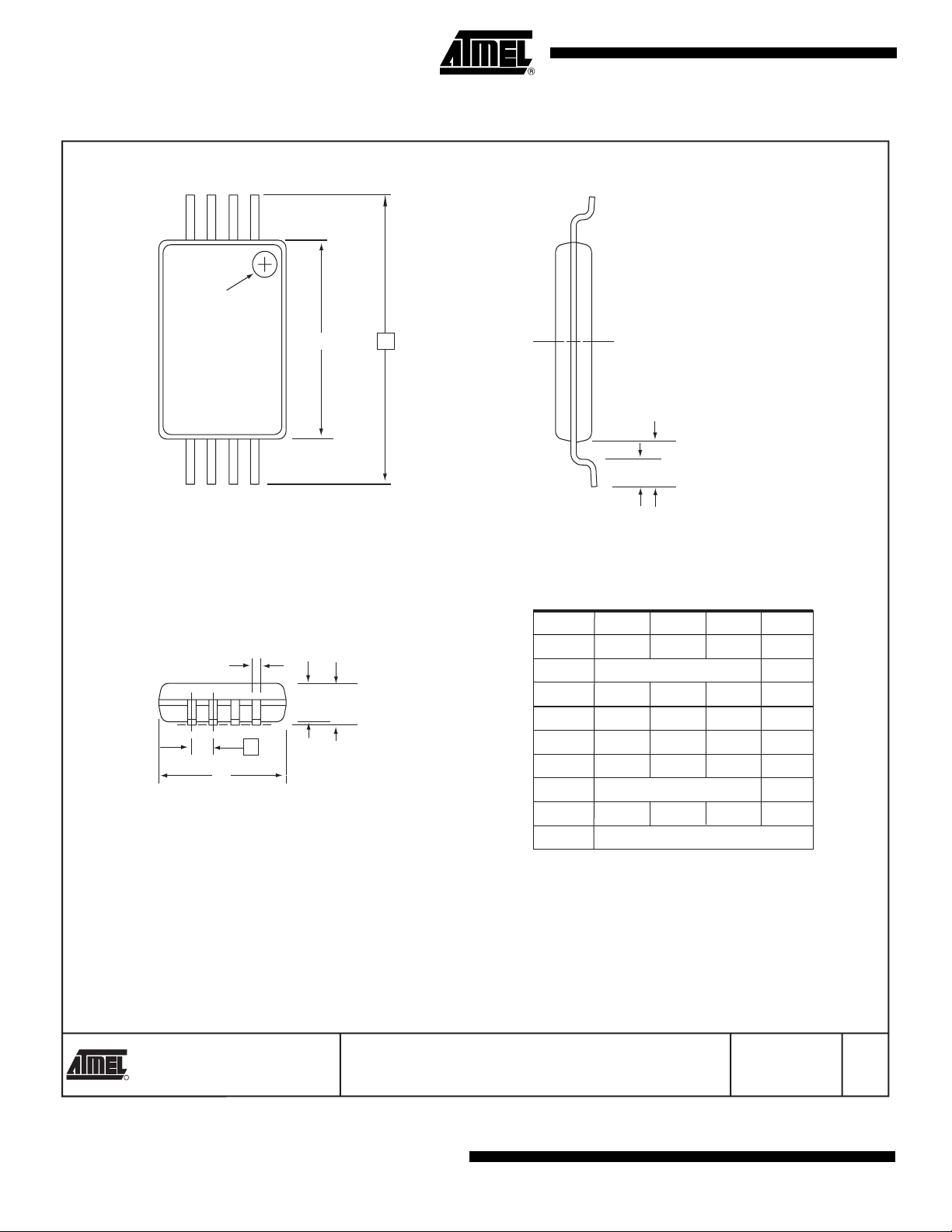
Packaging Information
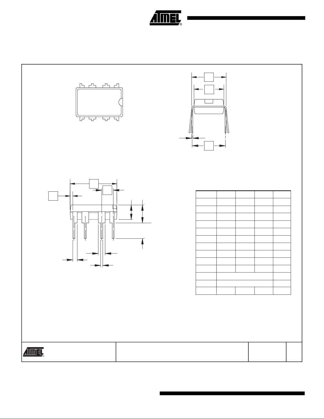
8P3 – PDIP
D1
b3
4 PLCS
Top View
D
e
Side View
1
E
E1
N
c
eA
End View
COMMON DIMENSIONS
(Unit of Measure = inches)
b
b2
A2 A
SYMBOL
A
A2 0.115 0.130 0.195
b 0.014 0.018 0.022 5
b2 0.045 0.060 0.070 6
b3 0.030 0.039 0.045 6
c 0.008 0.010 0.014
D 0.355 0.365 0.400 3
L
D1 0.005
E 0.300 0.310 0.325 4
E1 0.240 0.250 0.280 3
e 0.100 BSC
eA 0.300 BSC 4
L 0.115 0.130 0.150 2
MIN
NOM
–
MAX
–
0.210 2
–
–
3
NOTE
Notes: 1. This drawing is for general information only; refer to JEDEC Drawing MS-001, Variation BA, for additional information.
2. Dimensions A and L are measured with the package seated in JEDEC seating plane Gauge GS-3.
3. D, D1 and E1 dimensions do not include mold Flash or protrusions. Mold Flash or protrusions shall not exceed 0.010 inch.
4. E and eA measured with the leads constrained to be perpendicu
5. Pointed or rounded lead tips are preferred to ease insertion.
6. b2 and b3 maximum dimensions do not include Dambar protrusions. Dambar protrusions shall not exceed 0.010 (0.25 mm).
TITLE
8P3, 8-lead, 0.300" Wide Body, Plastic Dual
In-line Package (PDIP)
18
2325 Orchard Parkway
R
San Jose, CA 95131
AT24C01A/02/04/08A/16A
lar to datum.
DRAWING NO.
01/09/02
8P3
0180Z1–SEEPR–5/07
REV.
B

8S1 – JEDEC SOIC
AT24C01A/02/04/08A/16A
C
1
E
N
∅
E1
L
Top View
End View
e
D
Side View
B
A
SYMBOL
A1
A 1.35 – 1.75
A1 0.10 – 0.25
b 0.31 – 0.51
C 0.17 – 0.25
D 4.80 – 5.00
E1 3.81 – 3.99
E 5.79 – 6.20
e 1.27 BSC
L 0.40 – 1.27
∅ 0˚ – 8˚
COMMON DIMENSIONS
(Unit of Measure = mm)
MIN
NOM
MAX
NOTE
Note:
These drawings are for general information only. Refer to JEDEC Drawing MS-012, Variation AA for proper dimensions, tolerances, datums, etc.
1150 E. Cheyenne Mtn. Blvd.
Colorado Springs, CO 80906
R
0180Z1–SEEPR–5/07
TITLE
8S1, 8-lead (0.150" Wide Body), Plastic Gull Wing
Small Outline (JEDEC SOIC)
DRAWING NO.
8S1 B
10/7/03
REV.
19
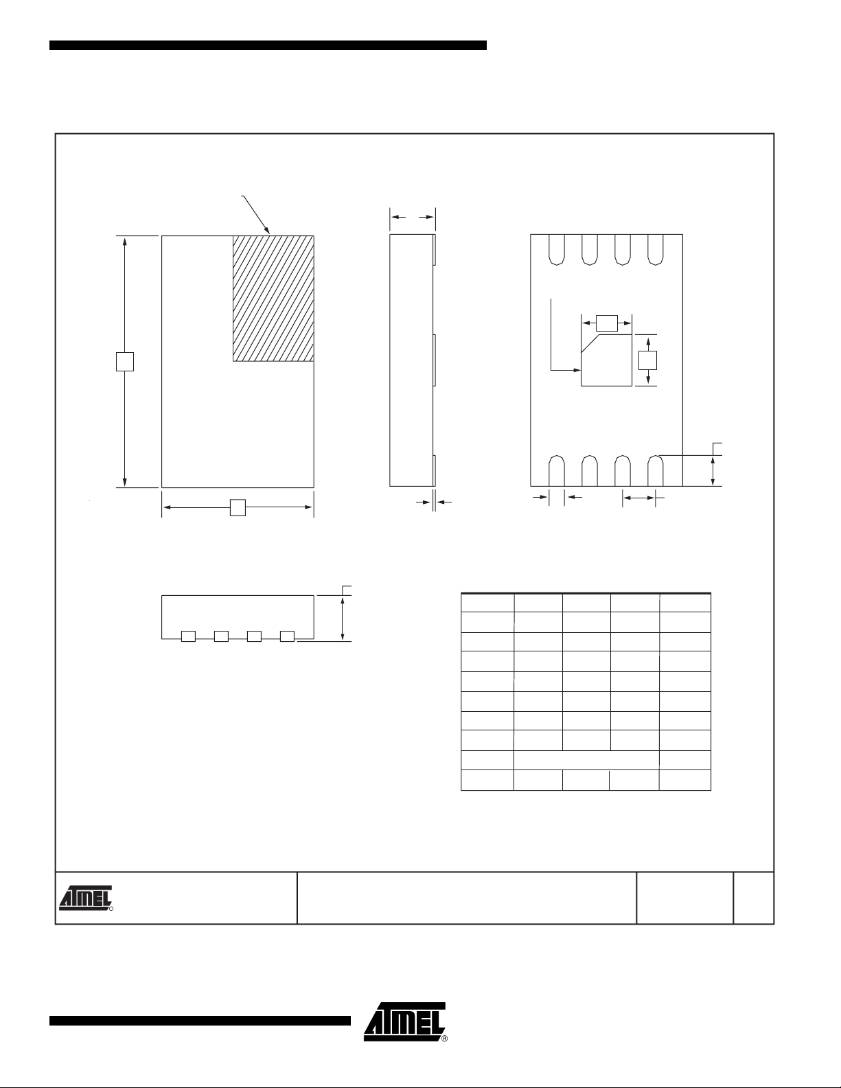
8A2 – TSSOP
Pin 1 indicator
this corner
123
N
Top View
b
e
D
Side View
A2
E1
E
L1
L
End View
COMMON DIMENSIONS
(Unit of Measure = mm)
SYMBOL
A
D 2.90 3.00 3.10 2, 5
E 6.40 BSC
E1 4.30 4.40 4.50 3, 5
A – – 1.20
A2 0.80 1.00 1.05
b 0.19 – 0.30 4
e 0.65 BSC
L 0.45 0.60 0.75
L1 1.00 REF
MIN
NOM
MAX
NOTE
Notes: 1. This drawing is for general information only. Refer to JEDEC Drawing MO-153, Variation AA, for proper dimensions, tolerances,
20
datums, etc.
2. Dimension D does not include mold Flash, protrusions or gate burrs. Mold Flash, protrusions and gate burrs shall not exceed
0.15 mm (0.006 in) per side.
3. Dimension E1 does not include inter-lead Flash or protrusions. Inter-lead Flash and protrusions shall not exceed 0.25 mm
(0.010 in) per side.
4. Dimension b does not include Dambar protrusion. Allowable Dambar protrusion shall be 0.08 mm total in excess of the
b dimension at maximum material condition. Dambar cannot be located on the lower radius of the foot. Minimum space between
protrusion and adjacent lead is 0.07 mm.
5. Dimension D and E1 to be determined at Datum Plane H.
DRAWING NO.
8A2
2325 Orchard Parkway
R
San Jose, CA 95131
TITLE
8A2, 8-lead, 4.4 mm Body, Plastic
Thin Shrink Small Outline Package (TSSOP)
AT24C01A/02/04/08A/16A
0180Z1–SEEPR–5/07
5/30/02
REV.
B
8Y1 – MAP
AT24C01A/02/04/08A/16A
PIN 1 INDEX AREA
A
1
PIN 1 INDEX AREA
3 4
2
E1
D
D1
L
E
Top View
Side View
A
End View
8
A1
SYMBOL
A – – 0.90
A1 0.00 – 0.05
D 4.70 4.90 5.10
E 2.80 3.00 3.20
D1 0.85 1.00 1.15
E1 0.85 1.00 1.15
b 0.25 0.30 0.35
e 0.65 TYP
L 0.50 0.60 0.70
b
COMMON DIMENSIONS
(Unit of Measure = mm)
MIN
NOM
6e5
7
Bottom View
MAX
NOTE
2325 Orchard Parkway
R
San Jose, CA 95131
0180Z1–SEEPR–5/07
TITLE
8Y1, 8-lead (4.90 x 3.00 mm Body) MSOP Array Package
(MAP) Y1
DRAWING NO.
8Y1
2/28/03
REV.
C
21
8Y6 − Mini-MAP (MLP 2x3 mm)
A
Pin 1
Index
Area
E
D
A2
A3
E2
A1
SYMBOL
D 2.00 BSC
E 3.00 BSC
D2 1.40 1.50 1.60
E2 - - 1.40
A - - 0.60
A1 0.0 0.02 0.05
A2 - - 0.55
A3 0.20 REF
L 0.20 0.30 0.40
e 0.50 BSC
b 0.20 0.25 0.30 2
D2
e (6X)
1.50 REF.
COMMON DIMENSIONS
(Unit of Measure = mm)
MIN
NOM
MAX
b
(8X)
Pin 1 ID
L (8X)
NOTE
Notes: 1. This drawing is for general information only. Refer to JEDEC Drawing MO-229, for proper dimensions,
tolerances, datums, etc.
2. Dimension b applies to metallized terminal and is measured between 0.15 mm and 0.30 mm from the terminal tip. If the
terminal has the optional radius on the other end of the terminal, the dimension should not be measured in that radius area.
TITLE
22
2325 Orchard Parkway
R
San Jose, CA 95131
AT24C01A/02/04/08A/16A
8Y6, 8-lead 2.0 x 3.0 mm Body, 0.50 mm Pitch, Utlra Thin Mini-Map,
Dual No Lead Package (DFN) ,(MLP 2x3)
DRAWING NO.
8Y6
0180Z1–SEEPR–5/07
8/26/05
REV.
C

5TS1 – SOT23
AT24C01A/02/04/08A/16A
e1
E1
5
4
E
C
C
L
L1
1
2
Top View
3
End View
b
A2
A
Seating
Plane
e
D
Side View
NOTES: 1. This drawing is for general information only. Refer to JEDEC Drawing
MO-193, Variation AB, for additional information.
2. Dimension D does not include mold flash, protrusions, or gate burrs.
Mold flash, protrusions, or gate burrs shall not exceed 0.15 mm per end.
Dimension E1 does not include interlead flash or protrusion. Interlead
flash or protrusion shall not exceed 0.15 mm per side.
3. The package top may be smaller than the package bottom. Dimensions
D and E1 are determined at the outermost extremes of the plastic body
exclusive of mold flash, tie bar burrs, gate burrs, and interlead flash, but
including any mismatch between the top and bottom of the plastic body.
4. These dimensions apply to the flat section of the lead between 0.08 mm
and 0.15 mm from the lead tip.
5. Dimension "b" does not include Dambar protrusion. Allowable Dambar
protrusion shall be 0.08 mm total in excess of the "b" dimension at
maximum material condition. The Dambar cannot be located on the lower
radius of the foot. Minimum space between protrusion and an adjacent lead
shall not be less than 0.07 mm.
1150 E. Cheyenne Mtn. Blvd.
R
Colorado Springs, CO 80906
TITLE
5TS1, 5-lead, 1.60 mm Body, Plastic Thin Shrink
Small Outline Package (SHRINK SOT)
A1
COMMON DIMENSIONS
(Unit of Measure = mm)
SYMBOL
A – – 1.10
A1 0.00 – 0.10
A2 0.70 0.90 1.00
c 0.08 – 0.20 4
D 2.90 BSC 2, 3
E 2.80 BSC 2, 3
E1 1.60 BSC 2, 3
L1 0.60 REF
e 0.95 BSC
e1 1.90 BSC
b 0.30 – 0.50 4, 5
MIN
NOM
MAX
DRAWING NO.
PO5TS1 A
NOTE
6/25/03
REV.
0180Z1–SEEPR–5/07
23

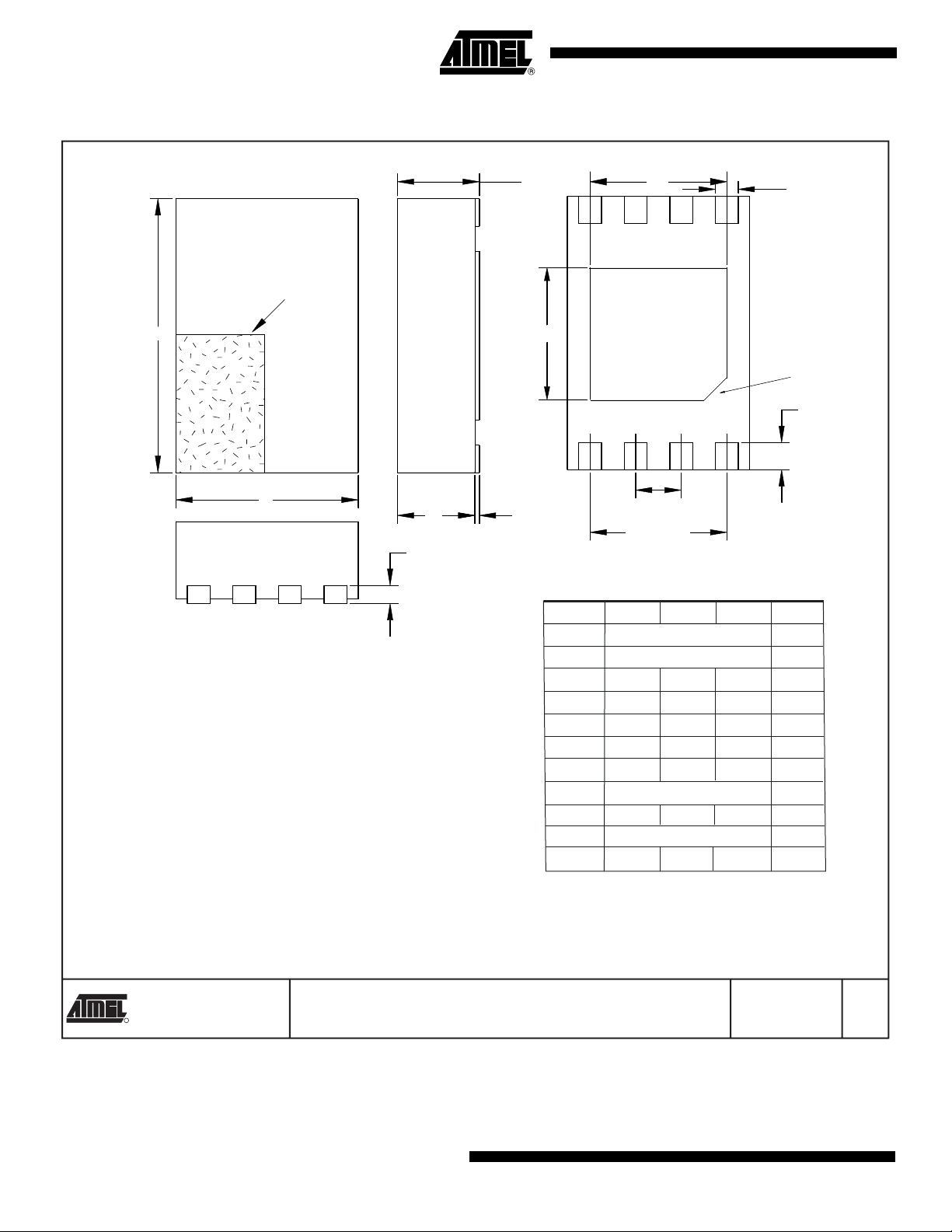
8U2 – dBGA2
ZM80.0
YXZM51.0
D
Top View
E
Pin 1 Mark
this corner
-Z-
8
1
2
7
3
6
Øb
d
4
5
D1
E1
e
A2
Bottom View
Side View
Notes: 1. These drawings are for general information only. No JEDEC Drawing to refer to for additional information.
2.
Dimension is measured at the maximum solder ball diameter, parallel to primary datum Z.
#
#
#
#
A
A1
SYMBOL
D 5.10
D1 1.43 TYP
E 3.25
E1 1.25 TYP
e 0.75 TYP
d 0.75 TYP
A 0.90 REF
A1 0.49 0.52 0.55
A2 0.35 0.38 0.41
Ø
COMMON DIMENSIONS
(Unit of Measure = mm)
MIN
b 0.47 0.50 0.53
NOM
TITLE
1150 E. Cheyenne Mtn. Blvd.
Colorado Springs, CO 80906
R
8U2, 8-ball 0.75 pitch, Die Ball Grid Array
Package (dBGA) AT24C512 (AT19870)
MAX
NOTE
02/04/02
DRAWING NO.
8U2 A
REV.
24
AT24C01A/02/04/08A/16A
0180Z1–SEEPR–5/07

8U3-1 – dBGA2
AT24C01A/02/04/08A/16A
E
D
PIN 1 BALL PAD CORNER
Top View
PIN 1 BALL PAD CORNER
2
31
4
(d1)
d
8
67
5
e
(e1)
Bottom View
8 SOLDER BALLS
1. Dimension “b” is measured at the maximum solder ball diameter.
This drawing is for general information only.
A
2
A
Side View
COMMON DIMENSIONS
(Unit of Measure = mm)
SYMBOL
A 0.71 0.81 0.91
A1 0.10 0.15 0.20
A2 0.40 0.45 0.50
b 0.20 0.25 0.30
D 1.50 BSC
E 2.00 BSC
e 0.50 BSC
e1 0.25 REF
d 1.00 BSC
d1 0.25 REF
MIN
NOM
1.
b
A
1
MAX
NOTE
R
0180Z1–SEEPR–5/07
1150 E. Cheyenne Mtn. Blvd.
Colorado Springs, CO 80906
TITLE
8U3-1, 8-ball, 1.50 x 2.00 mm Body, 0.50 mm pitch,
Small Die Ball Grid Array Package (dBGA2)
DRAWING NO.
PO8U3-1 A
6/24/03
REV.
25

Revision History
Doc. No. Date Comments
0180Z1 5/2007 Implemented revision history.
Changed formatting on page 16
26
AT24C01A/02/04/08A/16A
0180Z1–SEEPR–5/07

Atmel Corporation Atmel Operations
2325 Orchard Parkway
San Jose, CA 95131, USA
Tel: 1(408) 441-0311
Fax: 1(408) 487-2600
Regional Headquarters
Europe
Atmel Sarl
Route des Arsenaux 41
Case Postale 80
CH-1705 Fribourg
Switzerland
Tel: (41) 26-426-5555
Fax: (41) 26-426-5500
Asia
Room 1219
Chinachem Golden Plaza
77 Mody Road Tsimshatsui
East Kowloon
Hong Kong
Tel: (852) 2721-9778
Fax: (852) 2722-1369
Japan
9F, Tonetsu Shinkawa Bldg.
1-24-8 Shinkawa
Chuo-ku, Tokyo 104-0033
Japan
Tel: (81) 3-3523-3551
Fax: (81) 3-3523-7581
Memory
2325 Orchard Parkway
San Jose, CA 95131, USA
Tel: 1(408) 441-0311
Fax: 1(408) 436-4314
Microcontrollers
2325 Orchard Parkway
San Jose, CA 95131, USA
Tel: 1(408) 441-0311
Fax: 1(408) 436-4314
La Chantrerie
BP 70602
44306 Nantes Cedex 3, France
Tel: (33) 2-40-18-18-18
Fax: (33) 2-40-18-19-60
ASIC/ASSP/Smart Cards
Zone Industrielle
13106 Rousset Cedex, France
Tel: (33) 4-42-53-60-00
Fax: (33) 4-42-53-60-01
1150 East Cheyenne Mtn. Blvd.
Colorado Springs, CO 80906, USA
Tel: 1(719) 576-3300
Fax: 1(719) 540-1759
Scottish Enterprise Technology Park
Maxwell Building
East Kilbride G75 0QR, Scotland
Tel: (44) 1355-803-000
Fax: (44) 1355-242-743
RF/Automotive
Theresienstrasse 2
Postfach 3535
74025 Heilbronn, Germany
Tel: (49) 71-31-67-0
Fax: (49) 71-31-67-2340
1150 East Cheyenne Mtn. Blvd.
Colorado Springs, CO 80906, USA
Tel: 1(719) 576-3300
Fax: 1(719) 540-1759
Biometrics/Imaging/Hi-Rel MPU/
High Speed Converters/RF Datacom
Avenue de Rochepleine
BP 123
38521 Saint-Egreve Cedex, France
Tel: (33) 4-76-58-30-00
Fax: (33) 4-76-58-34-80
Literature Requests
www.atmel.com/literature
Disclaimer: The information in this document is provided in connection with Atmel products. No license, express or implied, by estoppel or otherwise, to any
intellectual property right is granted by this document or in connection with the sale of Atmel products. EXCEPT AS SET FORTH IN ATMEL’S TERMS AND CONDI-
TIONS OF SALE LOCATED ON ATMEL’S WEB SITE, ATMEL ASSUMES NO LIABILITY WHATSOEVER AND DISCLAIMS ANY EXPRESS, IMPLIED OR STATUTORY
WARRANTY RELATING TO ITS PRODUCTS INCLUDING, BUT NOT LIMITED TO, THE IMPLIED WARRANTY OF MERCHANTABILITY, FITNESS FOR A PARTICULAR
PURPOSE, OR NON-INFRINGEMENT. IN NO EVENT SHALL ATMEL BE LIABLE FOR ANY DIRECT, INDIRECT, CONSEQUENTIAL, PUNITIVE, SPECIAL OR INCIDENTAL DAMAGES (INCLUDING, WITHOUT LIMITATION, DAMAGES FOR LOSS OF PROFITS, BUSINESS INTERRUPTION, OR LOSS OF INFORMATION) ARISING OUT
OF THE USE OR INABILITY TO USE THIS DOCUMENT, EVEN IF ATMEL HAS BEEN ADVISED OF THE POSSIBILITY OF SUCH DAMAGES. Atmel makes no
representations or warranties with respect to the accuracy or completeness of the contents of this document and reserves the right to make changes to specifications
and product descriptions at any time without notice. Atmel does not make any commitment to update the information contained herein. Unless specifically provided
otherwise, Atmel products are not suitable for, and shall not be used in, automotive applications. Atmel’s products are not intended, authorized, or warranted for use
as components in applications intended to support or sustain life.
© 2007 Atmel Corporation. All rights reserved. Atmel®, logo and combinations thereof and others, are registered trademarks or trademarks of
Atmel Corporation or its subsidiaries. Other terms and product names may be trademarks of others.
Printed on recycled paper.
0180Z1–SEEPR–5/07

 Loading...