

ATMEL AT24C01-10TI-2.7, AT24C01-10TI-2.5, AT24C01-10TI-1.8, AT24C01-10TI, AT24C01-10TC-2.7 Datasheet
...
Features
•
Low Voltage and Standard Voltage Operation
– 5.0 (VCC = 4.5V to 5.5V)
– 2.7 (VCC = 2.7V to 5.5V)
– 2.5 (VCC = 2.5V to 5.5V)
– 1.8 (VCC = 1.8V to 5.5V)
•
Internally Organized 128 x 8
•
2-Wire Serial Interface
•
Bidirectional Data Transfer Protocol
•
100 kHz (1.8V, 2.5V, 2.7V) and 400 kHz (5V) Compatibility
•
4-Byte Page Write Mode
•
Self-Timed Write Cycle (10 ms max)
•
High Reliability
– Endurance: 1 Million Write Cycles
– Data Retention: 100 Years
– ESD Protection: >3000V
•
Automotive Grade and Extended Temperature Devices Available
•
8-Pin PDIP, 8-Pin MSOP, 8-Pin TSSOP and 8-Pin JEDEC SOIC Packages
2-Wire Serial
EEPROM
1K (128 x 8)
Description
The AT24C01 provides 1024 bits of serial electrically erasable and programmable
read only memory (EEPROM) organized as 128 words of 8 bits each. The device is
optimized for use in many industri al and comm ercial ap plicatio ns wher e low power
and low voltage operation are essential. The AT24C01 is available in space saving
8-pin PDIP, 8-pin MSOP, 8-pin TSSOP , and 8-pin JEDEC SOIC pac kages and is
accessed via a 2-wire serial interface. In addition, the entire family is available in 5.0V
(4.5V to 5.5V), 2.7V (2.7V to 5.5V), 2.5V (2.5V to 5.5V) and 1.8V (1.8V to 5.5V) versions.
Pin Configurations
Pin Name Function
NC No Connect
SDA Serial Data
SCL Serial Clock Input
Test Test Input (GND or V
8-Pin PDIP
CC
NC
NC
NC
GND
)
8-Pin MSOP
8-Pin TSSOP
1
2
3
4
8-Pin SOIC
8
VCC
7
TEST
6
SCL
5
SDA
AT24C01
2-Wire, 1K
Serial EEPROM
NC
NC
NC
GND
1
2
3
4
8
VCC
7
TEST
6
SCL
5
SDA
NC
NC
NC
GND
1
2
3
4
VCC
8
TEST
7
SCL
6
SDA
5
Rev. 0134C–07/98
1
Absolute Maximum Ratings*
Operating Temperature.................................. -55°C to +125°C
Storage Temperature..................................... -65°C to +150°C
Voltage on Any Pin
with Respect to Ground.....................................-1.0V to +7.0V
Maximum Operating Voltage........................................... 6.25V
DC Output Current........................................................5.0 mA
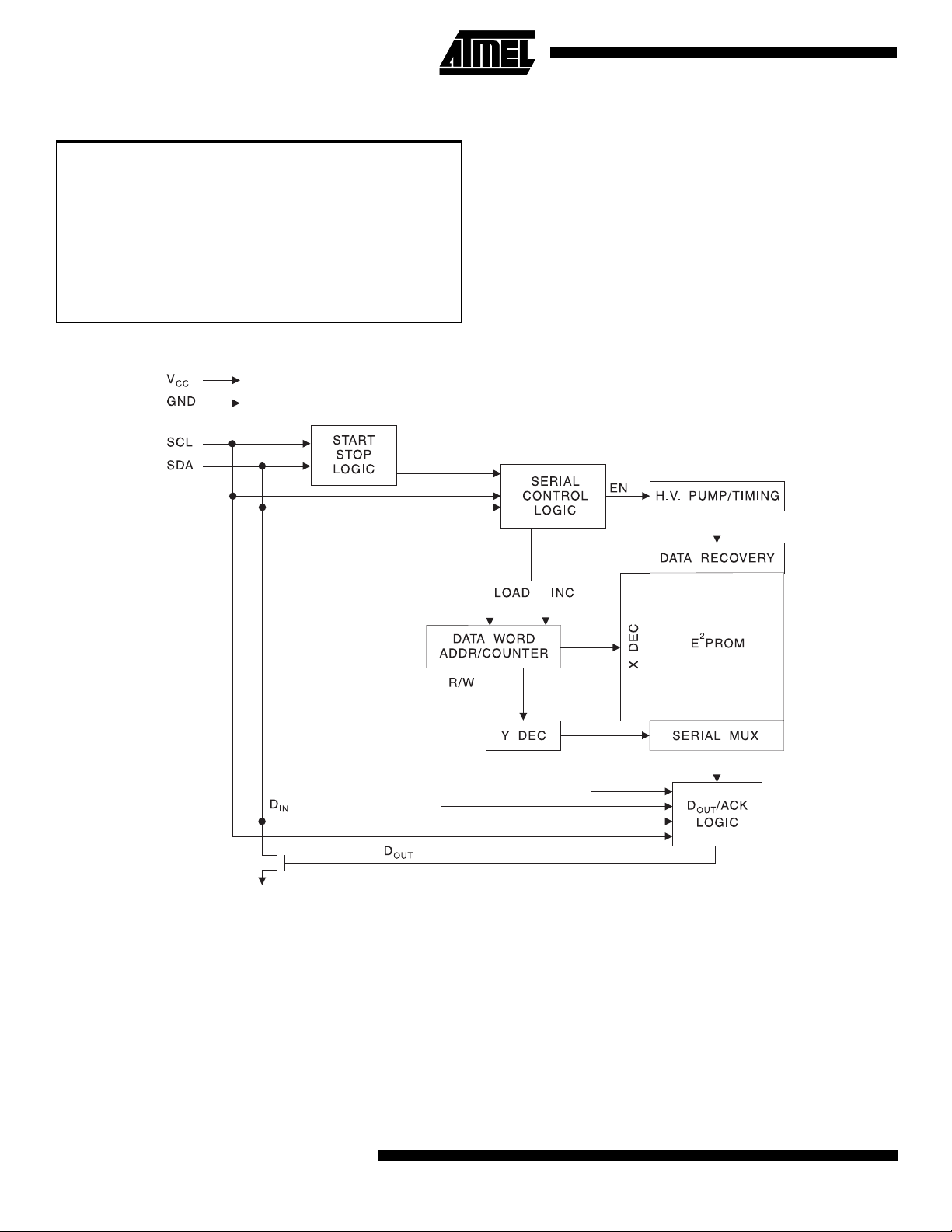
Block Diagram
*NOTICE: Stresses beyond those listed under “Absolute
Maximum Ratings” may cause permanent damage to the de vic e. T his is a stres s r ating o nly an d
functional opera tion of the device at these or an y
other conditions beyond those indicated in the
operational sections of this specification is not
implied. Exposure to absolute maximum rating
conditions for extended periods may affect
device reli abi li ty.
Pin Description
SERIAL CLOCK (SCL):
edge clock data into each EEPROM device and negative
edge clock data out of each device.
SERIAL DATA (SDA):
serial data transfer. This pin is open-drain driven and may
be wire-ORed with any number of other open-drain or open
collector devices.
2
The SCL input is used to positive
The SDA pin is bidirectional for
AT24C01
Memory Organization
AT24C01, 1K SERIAL EEPROM:
128 pages of 1 byte each. The 1K requires a 7-bit data
word address for random word addressing.
Internally organiz ed wi th
AT24C01
Pin Capacitance
Applicable over recommended operating range from TA = 25°C, f = 1.0 MHz, VCC = +1.8V.
Symbol T est Condit ion Max Units Condition
C
I/O
C
IN
DC Characteristics
Applicable over recommend ed operating range from: TAI = -40°C to +85°C, VCC = +1.8V to +5.5V, TAC = 0°C to +70°C,
= +1.8V to +5.5V (unless otherwise noted).
V
CC
Symbol Parameter Test Condition Min Typ Max Units
Input/Output Capacitance (SDA) 8 pF V
I/O
= 0V
Input Capacitance (A0, A1, A2, SCL) 6 pF VIN = 0V
V
V
V
V
I
I
I
I
I
I
I
I
V
V
V
V
CC1
CC2
CC3
CC4
CC
CC
SB1
SB2
SB3
SB4
LI
LO
IL
IH
OL2
OL1
Supply Voltage 1.8 5.5 V
Supply Voltage 2.5 5.5 V
Supply Voltage 2.7 5.5 V
Supply Voltage 4.5 5.5 V
Supply Current VCC = 5.0V READ at 100 KHz 0.4 1.0 mA
Supply Current VCC = 5.0V WRITE at 100 KHz 2.0 3.0 mA
Standby Current VCC = 1.8V VIN = VCC or V
Standby Current VCC = 2.5V VIN = VCC or V
Standby Current V
= 2.7V VIN = VCC or V
CC
Standby Current VCC = 5.0V VIN = VCC or V
Input Leakage Current VIN = VCC or V
Output Leakage Current V
Input Low Level
Input High Level
(1)
(1)
OUT
= V
CC
SS
SS
SS
SS
SS
or V
Output Low Level VCC = 3.0V IOL = 2.1 mA 0.4 V
Output Low Level VCC = 1.8V IOL = 0.15 mA 0.2 V
Note: 1. VIL min and VIH max are reference only and are not tested.
SS
0.6 3.0
1.4 4.0
1.6 4.0
8.0 18.0
0.10 3.0
0.05 3.0
µ
µ
µ
µ
µ
µ
-0.6 VCC × 0.3 V
VCC × 0.7 VCC + 0.5 V
A
A
A
A
A
A
3

AC Characteristics
Applicable over recomme nded operating r ange from TA = -40°C to +85°C, VCC = +1.8V to +5.5V, CL = 1 TTL Gate and
100 pF (unless otherwise noted).
2.7-, 2.5-, 1.8-volt 5.0-volt
Symbol Parameter
f
SCL
t
LOW
t
HIGH
t
I
t
AA
t
BUF
t
HD.STA
t
SU.STA
t
HD.DAT
t
SU.DAT
t
R
t
F
t
SU.STO
t
DH
t
WR
Endurance
Note: 1. This parameter is characterized and is not 100% tested.
(1)
Clock Frequency, SCL 100 400 KHz
Clock Pulse Width Low 4.7 1.2
Clock Pulse Width High 4.0 0.6
Noise Suppression Time
Clock Low to Data Out Valid 0.1 4.5 0.1 0.9
Time the bus must be free before a new
transmission can start
Start Hold Time 4.0 0.6
Start Set-up Time 4.7 0.6
Data In Hold Time 0 0
Data In Set-up Time 200 100 ns
Inputs Rise Time
Inputs Fall Time
Stop Set-up Time 4.7 0.6
Data Out Hold Time 100 50 ns
Write Cycle Time 10 10 ms
5.0V, 25°C, Page Mode 1M 1M
(1)
(1)
(1)
(1)
100 50 ns
4.7 1.2
1.0 0.3
300 300 ns
UnitsMin Max Min Max
µ
s
µ
s
µ
s
µ
s
µ
s
µ
s
µ
s
µ
s
µ
s
Write
Cycles
Device Operation
CLOCK and DATA TRANSITIONS:
mally pulled high wi th an ex ter na l dev ic e. Dat a o n t he SDA
pin may chan ge o nly duri ng S CL l ow t ime per iods (refe r t o
Data Validity timing diagram). Data changes during S CL
high periods will indicate a start or stop condition as
defined below.
START CONDITION:
A high-to-low transition of SDA with
SCL high is a start condition which must precede any other
command (refer to Start and Stop Definition timing diagram).
STOP CONDITION:
A low-to-high transition of SDA with
SCL high is a stop condition which terminates all communications. After a read sequence, the stop comm and will
place the EEPROM in a standby power mode (refer to Start
and Stop Definition timing diagram).
ACKNOWLEDGE:
All addresses and data words are serially transmitted to and from the EEPROM in 8-bit words.
Any device on the system bus receiving data (w hen com-
4
AT24C01
The SDA pin is nor-
municating with the EEPROM) must pull the SDA bus low
to acknowledge that it has successfully received each
word. This must happen during the ninth clock cycle after
each word received and after all other system devices have
freed the SDA bus. The EEPROM will likewise ackno wledge by pulling SDA low after receiving each address or
data word (refer to Acknowledge Response from Receiver
timing diagram).
STANDBY MODE:
The AT24C01 features a low power
standby mode which is enabled: (a) upon power-up and (b)
after the receipt of the STOP bit and the completi on of any
internal operations.
MEMORY RESET:
After an interruption in protocol, power
loss or system reset, any 2-wire part can be reset by following these steps:
(a) Clock up to 9 cycles, (b) look for SDA high in each cycle
while SCL is high and then (c) create a start condition as
SDA is high.

Bus Timing
SCL: Serial Clock, SDA: Serial Data I/O
Write Cycle Timing
SCL: Serial Clock, SDA: Serial Data I/O
AT24C01
SCL
SDA
Note: 1. The write cycle time tWR is the time from a valid stop condition of a write sequence to the end of the internal clear/write
cycle.
8th BIT ACK
WORD n
STOP
CONDITION
t
(1)
WR
START
CONDITION
5

Data Validity
Start and Stop Definition
Output Acknowledge
6
AT24C01

AT24C01
Write Operations
BYTE WRITE:
requires a 7-bit data word address and a low write bit. Upon
receipt of this address, th e EEPROM will again respond
with a zero and then clock in the first 8-bit data word. Following receipt of the 8-b it da ta wo rd, the EE PROM will output a zero and the addressing device, such as a
microcontroller, must te rminate th e write sequ ence with a
stop condition. At this time the EEPROM enters an internally-timed write cycle to the nonvolatile memory. All inputs
are disabled during this wr ite cycl e , t
will not respond until the write is complete (refer to Figure
1).
PAGE WRITE:
write.
A page write is initiated the same as a byte write but the
microcontroller does not send a stop condition after the first
data word is clocked in. Instead, after the EEPROM
acknowledges receipt of the first data word, the microcontroller can transmit up to three more d ata words. Th e
EEPROM will respond with a zero after each data word
received. Th e microcontr oller must ter minate the pag e
write sequence with a stop condition (refer to Figure 2).
The data word address lower 2 bits are internally incremented following the rece ipt of each data word. The hig her
five data word address bits are not incremented, retaining
the memory page row location. When the word address,
internally ge nerated, r eaches th e page boun dary, the fo llowing byte is pla ced at th e be ginnin g o f the same pa ge. If
more than four data words are transmitted to the EEPROM,
the data word address will “roll ov er” and previ ous data will
be overwritten.
ACKNOWLEDGE POLLING:
write cycle has started and the EEPROM inputs are disabled, acknowledge polling can be initiated. T his invol ves
sending a start condition followed by the device address
word. The read/write bit is repres entative of the operation
desired. Only if the internal write cycle has completed will
the EEPROM respond with a zero allowing the read or
write sequence to continue.
Following a start condition, a write operation
, and the EEPROM
WR
The AT24C01 is capable of a 4-byte page
Once the internally-time d
Read Operations
Read operations are initiated the same way as write operations with the exception that the read/write select bit in the
device address word is set to one. There are two read
operations: byte read and sequential read.
BYTE READ:
followed by a 7-bit data word address and a high read bit.
The AT24C01 will respond with an acknowledge and then
serially output 8 data bits. The microcontroller does not
respond with a zero but does generate a following stop
condition (refer to Figure 3).
SEQUENTIAL READ:
same as a byt e rea d. Aft er the m icroc ontr oller rece ives a n
8-bit data word, it responds with an acknowledge. As long
as the EEPROM receives an acknowledge, it will continue
to increment the data w ord address and seria lly clock out
sequential data words. Whe n the memory addr ess limit is
reached, the data word address will “roll over” and the
sequential read will continue. The sequential read operation is terminated whe n the microcontroller does not
respond with an input zero but does generate a following
stop condition (refer to Figure 4).
A byte read is initiated with a start condition
Sequential read s are initiate d the
Figure 1.
Byte Write
7

Figure 2.
Page Write
Figure 3.
Figure 4.
Byte Read
Sequential Read
8
AT24C01

Ordering Information
tWR (max)
(ms)
10 3000 18 400 AT24C01-10PC
10 1500 4 100 AT24C01-10PC-2.7
10 1000 4 100 AT24C01-10PC-2.5
10 800 3 100 AT24C01-10PC-1.8
ICC (max)
(µA)
3000 18 400 AT24C01-10PI
1500 4 100 AT24C01-10PI-2.7
1000 4 100 AT24C01-10PI-2.5
800 3 100 AT24C01-10PI-1.8
ISB (max)
(µA)
f
MAX
(kHz) Ordering Code Package Operation Range
AT24C01-10SC
AT24C01-10MC
AT24C01-10TC
AT24C01-10SI
AT24C01-10MI
AT24C01-10TI
AT24C01-10SC-2.7
AT24C01-10MC-2.7
AT24C01-10TC-2.7
AT24C01-10SI-2.7
AT24C01-10MI-2.7
AT24C01-10TI-2.7
AT24C01-10SC-2.5
AT24C01-10MC-2.5
AT24C01-10TC-2.5
AT24C01-10SI-2.5
AT24C01-10MI-2.5
AT24C01-10TI-2.5
AT24C01-10SC-1.8
AT24C01-10MC-1.8
AT24C01-10TC-1.8
AT24C01-10SI-1.8
AT24C01-10MI-1.8
AT24C01-10TI-1.8
AT24C01
8P3
8S1
8M
8T
8P3
8S1
8M
8T
8P3
8S1
8M
8T
8P3
8S1
8M
8T
8P3
8S1
8M
8T
8P3
8S1
8M
8T
8P3
8S1
8M
8T
8P3
8S1
8M
8T
Commercial
(0°C to 70°C)
Industrial
(-40°C to 85°C)
Commercial
(0°C to 70°C)
Industrial
(-40°C to 85°C)
Commercial
(0°C to 70°C)
Industrial
(-40°C to 85°C)
Commercial
(0°C to 70°C)
Industrial
(-40°C to 85°C)
Package Type
8M 8-Lead, 0.118” Wide, Miniature Small Outline Package (MSOP)
8P3 8-Lead, 0.300" Wide, Plastic Dual Inline Package (PDIP)
8S1 8-Lead, 0.150" Wide, Plastic Gull Wing Small Outline (JEDEC SOIC)
8T 8-Lead, 0.170” Wide, Thin Shrink Small Outline Package (TSSOP)
Options
Blank Standard Operation (4.5V to 5.5V)
-2.7 Low-Voltage (2.7V to 5.5V)
-2.5 Low-Voltage (2.5V to 5.5V)
-1.8 Low-Voltage (1.8V to 5.5V)
9

Packaging Information
8M,
8-Lead, 0.118” Wide, Miniature Small Outline
Package (MSOP)
0.40 (0.016)
0.25 (0.010)
3.10 (0.122)
PIN 1
3.10 (0.122)
2.90 (0.114)
0.15 (0.006)
0.05 (0.002)
3.81
(0.150)
REF
4.90 (0.193)
REF
2.90 (0.114)
0.65 (0.026) TYP
1.10 (0.043)
0.97 (0.038)
0.23 (0.009)
0.13 (0.005)
8P3
, 8-Lead, 0.300” Wide, Plastic Dual Inline
Package (PDIP)
Dimensions in Inches and (Millimeters)
JEDEC STANDARD MS-001 BA
.400 (10.16)
.355 (9.02)
PIN
1
.280 (7.11)
.240 (6.10)
.037 (.940)
.300 (7.62) REF
.210 (5.33) MAX
SEATING
PLANE
.150 (3.81)
.115 (2.92)
.012 (.305)
.008 (.203)
.070 (1.78)
.045 (1.14)
.027 (.690)
.100 (2.54) BSC
.015 (.380) MIN
.022 (.559)
.014 (.356)
.325 (8.26)
.300 (7.62)
0
REF
15
.430 (10.9) MAX
8S1
, 8-Lead, 0.150” Wide, Plastic Gull Wing Small
Outline (JEDEC SOIC)
Dimensions in Inches and (Millimeters)
.020 (.508)
.013 (.330)
.244 (6.20)
.228 (5.79)
.068 (1.73)
.053 (1.35)
.010 (.254)
.007 (.203)
PIN 1
0
8
.157 (3.99)
.150 (3.81)
.050 (1.27) BSC
.196 (4.98)
.189 (4.80)
.010 (.254)
.004 (.102)
REF
.050 (1.27)
.016 (.406)
8T
, 8-Lead 0.170” Wide, Thin Shrink Small Outline
Package (TSSOP)
Dimensions in Millimeters and (Inches)*
PIN 1
6.50 (.256)
6.25 (.246)
0.30 (.012)
0.19 (.008)
3.10 (.122)
0
REF
8
2.90 (.114)
0.15 (.006)
0.05 (.002)
4.5 (.177)
4.3 (.169)
0.75 (.030)
0.45 (.018)
1.20 (.047) MAX
0.20 (.008)
0.09 (.004)
1.05 (.041)
0.80 (.033)
.65 (.026) BSC
*Controlling dimension: millimeters
10
AT24C01
 Loading...