

Datasheet AT22LV10-25PI, AT22LV10-25JI, AT22LV10-20SI, AT22LV10-20SC, AT22LV10-20PI Datasheet (ATMEL)
...
Features
•
Low V oltage Programmable Logic Device
– Wide Power Supply Range - 3.0V to 5.5V
– Ideal for Battery Powered Systems
•
High Speed Operation
– 20 ns max Propagation Delay at V
•
Commercial and Industrial Temperature Ranges
•
Familiar 22V10 Logic Architecture
•
Low Power 3-Volt CMOS Operation
CC
= 3.0V
AT22LV10L AT22LV10
Temp Com./Ind. Com./Ind.
(mA) 4 / 5 35 / 45
I
CC
•
CMOS and TTL Compatible Inputs and Outputs
–10 µA Leakage Maximum
•
Reprogrammable - Tested 100% for Programmability
•
High Reliability CMOS Technology
– 2000V ESD Protection
– 200 mA Latchup Immunity
•
Dual-In-Line and Surface Mount Packages
V
= 3.6V
CC
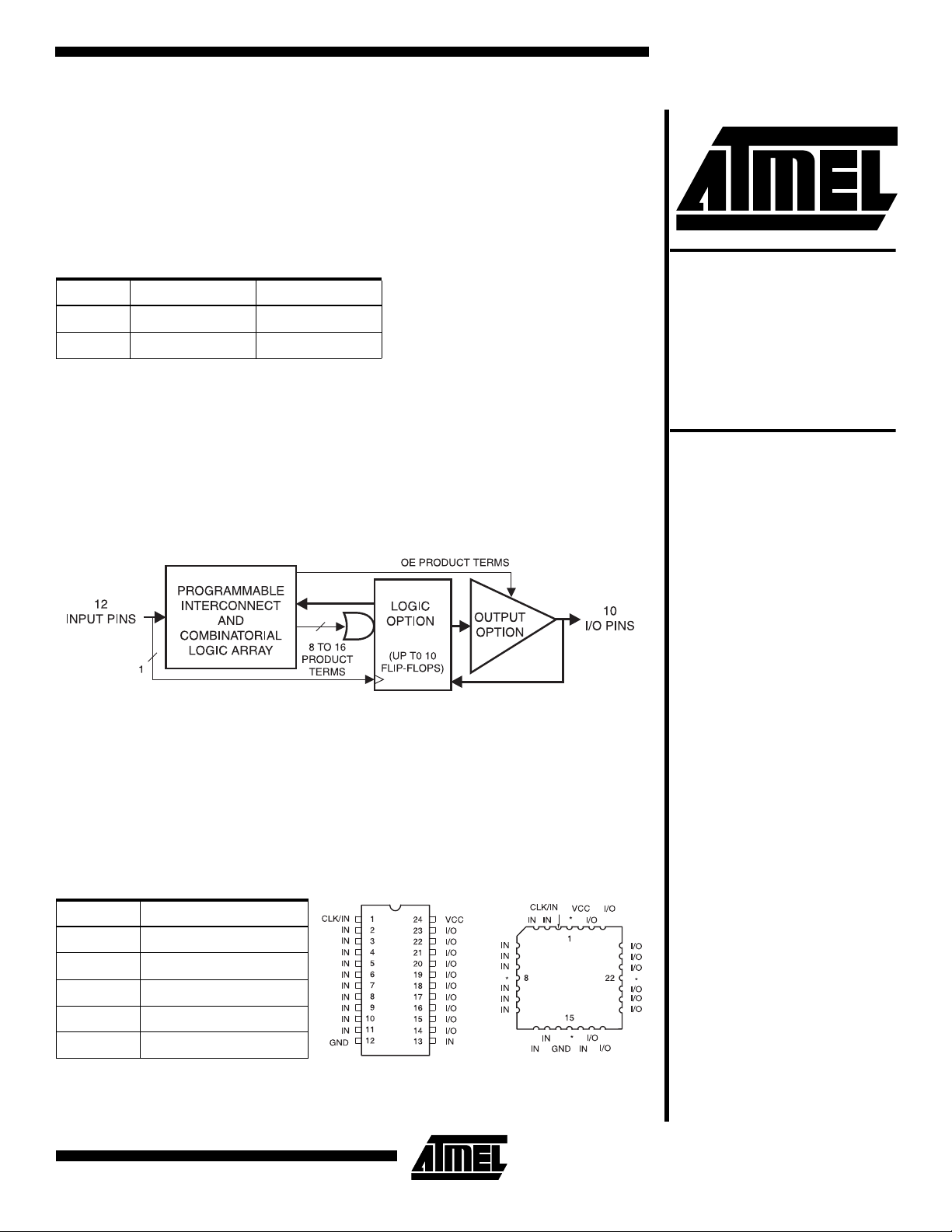
Logic Diagram
Description
The AT22LV10 and AT22LV10L are low volta ge compat ible CMO S high perfor mance
Programmable Logic Devices (PLDs). Speeds down to 20 ns and po wer dissipation
as low as 14.4 mW ar e offered . All sp eed rang es are spe cifi ed over th e 3.0V to 5. 5V
range. All pins offer a low ±10 µA leakage.
(continued)
Low-Voltage UV
Erasable
Programmable
Logic Device
AT22LV10
AT22LV10L
Pin Configurations
Pin Name Function
CLK/IN Clock and Logic Input
IN Logic Inputs
I/O Bidirectional Buffers
* No Internal Connection
VCC 3.0V to 5.5V Supply
DIP/SOIC PLCC
Rev. 0190C— 05/98
1
The AT22LV10L provides the optimum low power CMOS
PLD solution, with lo w DC power (1 mA typical at V
CC
=
3.3V) and full CMOS output le ve ls. The AT2 2LV 10L sig ni ficantly reduces total system power, allowing battery powered operation.
Full CMOS output levels help reduce power in many other
system components.
The AT22LV10 and AT22LV10L logic architectures ar e
identical to the familiar 22V10. Each output is allocated
from eight to 16 product terms, which allows highly complex logic functions to be realized.
Two additional product terms are included to provide synchronous preset an d asy nchr onous r eset . These te rms ar e
common to all ten registers. All registers are automatically
cleared upon power up.
Register pr el o ad sim p li fi e s te s ti n g. A secu r i ty fu se pr e v en ts
unauthorized copying of programmed fuse patterns.
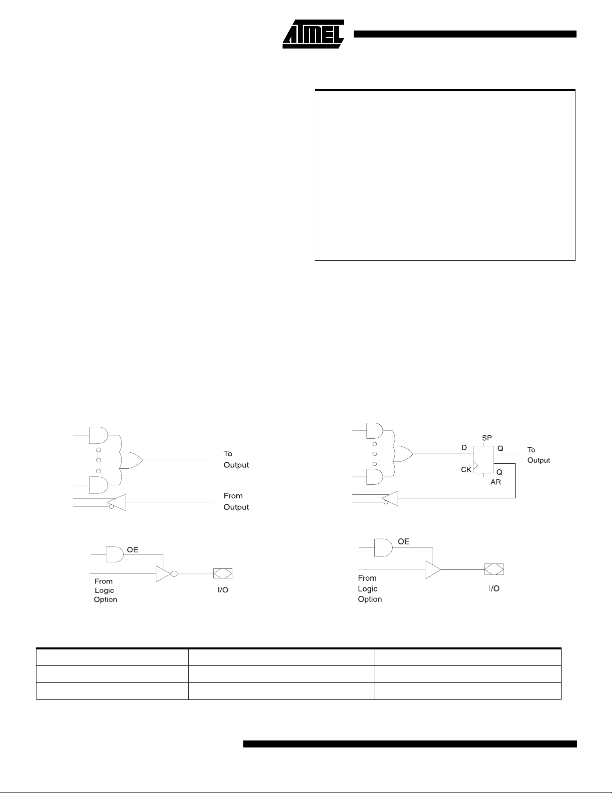
Logic Options
Absolute Maximum Ratings*
Temperature Under Bias................................-55°C to +125°C
Storage Temperature .....................................-65°C to +150°C
Voltage on Any Pin with
Respect to Ground........................................-2.0V to +7.0V
Voltage on Input Pins
with Respect to Ground
During Programming...................................-2.0V to +14.0V
Programming Voltage with
Respect to Ground......................................-2.0V to +14.0V
Integrated UV Erase Dose............................. 7258 W•sec/cm
*NOTICE: Stresses beyond those listed under “Absolute Maxi-
mum Ratings” ma y cause permanent d amage to th e
device. This is a stress rating only and functional
operation of the device at these or any other conditions beyond those indicated in the operational sections of this specif ication is not implie d. Exposure to
absolute maximum rating conditions for extended
periods may affect device reliability.
Note: 1. Minimum voltage is -0.6V dc whihc may undershoot
to -2.0V for pulses of less than 20 ns. Maximum pin
voltage is V
+ 2.0V for pulses of less than 20 ns.
V
CC
+ 0.75V dc which may unders hoo t to
CC
(1)
(1)
(1)
2
Output Options
DC and AC Operating Conditions
Commercial Industrial
Operating Temperature (Case) 0°C - 70°C -40°C - 85°C
VCC Power Supply 3.0V to 5.5V 3.0V to 5.5V
2
AT22LV10(L)
AT22LV10(L)
DC Characteristics
Symbol Parameter Condition Min Typ Max Units
I
LI
I
LO
I
CC
Input Load Current VIN = -0.1V to VCC + 1V 10 µA
Output Leakage
Current
= -0.1V to VCC + 0.1V 10 µA
V
OUT
Com. 20/50 35/90 mA
AT22LV10
Ind. 20/50 45/100 mA
Com. 1/2 4/12 mA
AT22LV10L
Power Supply
Current
= 3.6V / 5.5V ,
V
CC
= GND,
V
IN
Outputs Open
Ind. 1/2 5/15 mA
(1)
I
OS
V
IL1
V
IL2
V
IH
Output Short Circuit
Current
Input Low Voltage 4.5V ≤ V
Input Low Voltage 3.0V ≤ V
= 0.5V -120 mA
V
OUT
5.5V -0.6 0.8 V
≤
CC
4.5V -0.6 0.6 V
<
CC
Input High Voltage 2.0 V
+ 0.75 V
CC
VCC = 3.0V Com.,Ind. IOL = 8 mA 0.5 V
V
OL
V
OH
Output Low Voltage
= VIH or V
V
IN
IL
Output High Voltage
V
= 4.5V Com.,Ind. IOL = 16 mA 0.5 V
CC
V
= 3.0V Com.,Ind. IOL = 6 mA 0.35 V
CC
= VIH or VIL,
V
IN
= 3.0V / 4.5V
V
CC
IOH = -100 µAV
I
= -0.4 mA / -4.0 mA 2.4 V
OH
- 0.3 V
CC
Note: 1. Not more than one output at a time should be shorted. Duration of short circuit test should not exceed 30 sec.
3
AC Characteristics for the AT22LV10
AT22LV10-20 AT22LV10-25
Symbol Parameter
t
PD
t
EA
t
ER
t
CF
tCOClock to Output 0 8 14 0 10 17 ns
Input or Feedback to NonRegistered Output
12 20 15 25 ns
Input to Output Enable 20 15 25 ns
Input to Output Disable 20 15 25 ns
Clock to Feedback 049059ns
UnitsMin Typ Max Min Typ Max
t
S
t
H
t
P
t
W
Input or Feedback Setup Time 10 6 12 7 ns
Hold Time 0 0 ns
Clock Period 10 12 ns
Clock Width 5 6 ns
External Feedback 1/(tS+tCO) 41.6 34.5 MHz
F
MAX
Internal Feedback 1/(tS + tCF) 52.6 47.6 MHz
No Feedback 1/(t
t
AW
Asynchronous Reset Width 20 12 25 15 ns
Asynchronous Reset,
t
AR
Synchronous Preset,
Recovery Time
t
AP
Asynchronous Reset to
Registered Output Reset
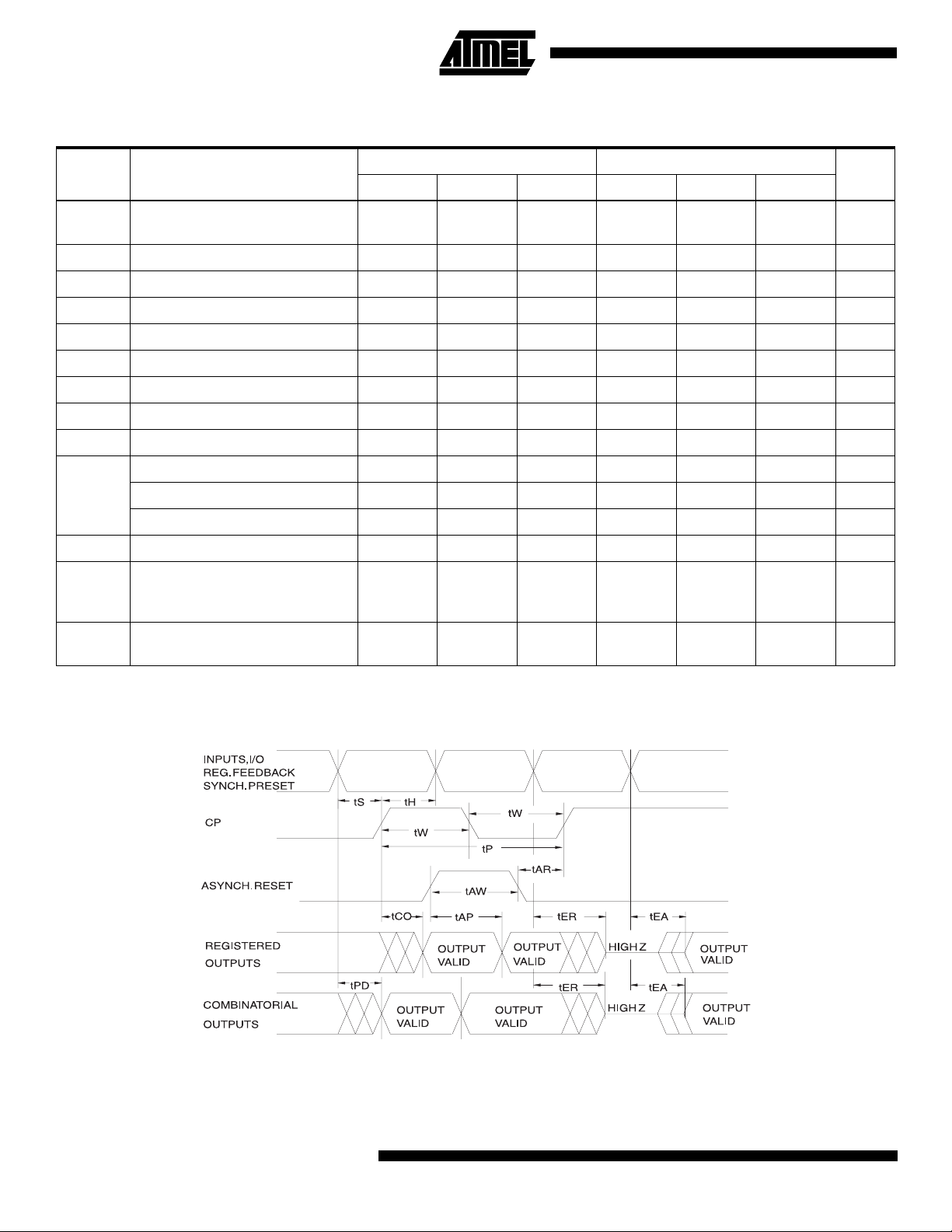
AC Waveforms
) 100.0 83.3 MHz
P
20 12 25 15 ns
15 25 18 28 ns
(1)
Note: 1. Timing measurement reference is 1.5V. Input AC driving levels are 0.0V and 3.0V, unless otherwise specified.
4
AT22LV10(L)

AC Characteristics for the AT22LV10L
Symbol Parameter
AT22LV10(L)
AT22LV10L-25
UnitsMin Typ Max
t
PD
t
EA
t
ER
t
CF
t
CO
t
SF
t
S
t
H
t
P
t
W
Input or Feedback to Non-Registered Output 15 25 ns
Input to Output Enable 15 25 ns
Input to Output Disable 15 25 ns
Clock to Feedback 0 5 9 ns
Clock to Output 0 10 14 ns
Feedback Setup Time 12 7 ns
Input Setup Time 17 15 ns
Hold Time 0 ns
Clock Period 12 ns
Clock Width 6 ns
External Feedback 1/(tS + tCO)32.2MHz
F
MAX
t
AW
t
AR
t
AP
Internal Feedback 1/(t
No Feedback 1/(t
+ tCF)47.6MHz
SF
) 83.3 MHz
P
Asynchronous Reset Width 25 15 ns
Asynchronous Reset Recovery Time 25 15 ns
Asynchronous Reset to Registered Output Reset 18 28 ns
Input Test Waveforms and
Measurement Levels
Output Test Loads:
Commercial
5

Functional Logic Diagram AT22LV10(L)
6
AT22LV10(L)

Preload of Registered Outputs
The registers in the AT22LV10 and AT22LV10L are provided with circuitry to allow loading of each r egister asy nchronously with either a high or a low. T his feature will
simplify testing since any state can be forced into the registers to control test sequencing. A V
will force the register high ; a V
IL
dent of the p olarity b it (C0) setting. The prel oad stat e is
entered by placing an 11.5V to 13V signal on pin 8 on
level on the I/O pin
IH
will force it low, indep en-
AT22LV10(L)
DIPs, and pin 10 on SMPs. When the clock pin is pulsed
high, the data on the I/O p ins is placed i nto the t en registers.
Level forc ed on registered output
pin during preload cycle
V
IH
V
IL
Register state after
cycle
High
Low
Power-Up Reset
The registers in the AT22LV10 and AT22LV10L are
designed to reset during power up. At a point delayed
slightly from VCC crossing 2.5V, all register s will be res et
to the low state. The output state will depend on the polarity
of the output buffer.
This feature is critical for state machine initialization. However, due to the asynchronous nature of reset and the
uncertainty of how VCC actually rises in the system, the following conditions are required:
1. The V
2. After reset occurs, all input and feedback setup
times must be met before driving the clock pin high,
and
3. The clock must remain stable during t
Pin Capacitance
C
IN
C
OUT
Note: 1. Typical values for nominal supply voltage. This parameter is only sampled and is not 100% tested.
rise must be monotonis;
CC
(f = 1 MHz, T = 25°C)
Parameter Description Min Typ Max Units
Power-Up
Reset Time
PR
t
PR
.
(1)
Typ Max Units Conditions
58pFV
68pFV
600 1000 ns
= 0V
IN
= 0V
OUT
Erasure Characteristics
The entire fuse array of an AT22LV10 or AT22LV10L is
erased after exposure to ult raviolet l ight at a wavelen gth o f
2537 Å. Complete erasure is assured after a minimum of
20 minutes exposur e using 12,00 0
spaced one inch away from the chip. Minimum erase time
for lamps at other intensity ratings can be calculated from
µW/cm
2
intensity lamps
•
the minimum inte grated erasur e dose of 1 5 W
sec/cm2. To
prevent unintentional erasure, an opaque label is recommended to cover the clear window on any UV erasable
PLD which will be subjected to continuous fluorescent
indoor lighting or sunligh t.
7

8
AT22LV10(L)

AT22LV10(L)
9

Ordering Information
t
PD
(ns)
20 10 14 AT22LV10-20JC
25 12 17 AT22LV10-25JC
25 17 14 AT22LV10L-25JC
t
S
(ns)
t
CO
(ns) Ordering Code Package Operation Range
AT22LV10-20PC
AT22LV10-20SC
AT22LV10-20JI
AT22LV10-20PI
AT22LV10-20SI
AT22LV10-25PC
AT22LV10-25SC
AT22LV10-25JI
AT22LV10-25PI
AT22LV10-25SI
AT22LV10L-25PC
AT22LV10L-25SC
AT22LV10L-25JI
AT22LV10L-25PI
AT22LV10L-25SI
28J
24P3
24S
28J
24P3
24S
28J
24P3
24S
28J
24P3
24S
28J
24P3
24S
28J
24P3
24S
Commercial
(0°C to 70°C)
Industrial
(-40°C to 85°C)
Commercial
(0°C to 70°C)
Industrial
(-40°C to 85°C)
Commercial
(0°C to 70°C)
Industrial
(-40°C to 85°C)
Package Type
28J 28-Lead, Plastic J-Leaded Chip Carrier OTP (PLCC)
24P3 24-Lead, 0.300" Wide, Plastic Dual Inline Package OTP (PDIP)
24S 24-Lead, 0.300" Wide, Plastic Gull Wing Small Outline OTP (SOIC)
10
AT22LV10(L)

Packaging Information
AT22LV10(L)
28J
, 28-Lead, Plastic J-Leaded Chip Carrier (PLCC)
Dimensions in Inches and (Millimeters)
JEDEC STANDARD MS-018 AB
.045(1.14) X 45°
.032(.813)
.026(.660)
.050(1.27) TYP
PIN NO.1
IDENTIFY
.045(1.14) X 30° - 45°
.456(11.6)
SQ
.450(11.4)
.495(12.6)
.485(12.3)
.300(7.62) REF SQ
.022(.559) X 45° MAX (3X)
SQ
.012(.305)
.008(.203)
.021(.533)
.013(.330)
.043(1.09)
.020(.508)
.120(3.05)
.090(2.29)
.180(4.57)
.165(4.19)
.430(10.9)
.390(9.91)
SQ
24P3
, 24-Lead, 0.300” Wide. Plastic Dual Inline
Package (PDIP)
Dimensions in Inches and (Millimeters)
JEDEC STANDARD MS-011 AB
1.27(32.3)
.200(5.06)
SEATING
PLANE
MAX
.151(3.84)
.125(3.18)
.110(2.79)
.090(2.29)
.012(.305)
.008(.203)
1.25(31.7)
1.100(27.94) REF
PIN
1
.065(1.65)
.040(1.02)
.325(8.26)
.300(7.62)
0
REF
15
.400(10.2) MAX
.023(.584)
.014(.356)
.266(6.76)
.250(6.35)
.090(2.29)
MAX
.005(.127)
MIN
.070(1.78)
.020(.508)
24S
, 24-Lead, 0.300” Wide, Plastic Gull Wing Small
Outline (SOIC)
Dimensions in Inches and (Millimeters)
.020(.508)
.013(.330)
PIN 1 ID
0
REF
8
.616(15.6)
.598(15.2)
.050(1.27) BSC
.012(.305)
.003(.076)
.050(1.27)
.015(.381)
.299(7.60)
.291(7.39)
.420(10.7)
.393(9.98)
.105(2.67)
.092(2.34)
.013(.330)
.009(.229)
11
 Loading...