

ATMEL AT17LV512A-10JI, AT17LV512A-10JC, AT17C010A-10JI, AT17C010A-10JC, AT17LV010A-10JI Datasheet
...
Features
•
Serial EEPROM Family for Configuring Altera FLEX
•
Simple, Easy-to-use 4-pin Interface
•
E2 Programmable 1M Bit Serial Memories Designed To Store Configuration Programs
For Programmable Gate Arrays
•
Cascadable To Support Additional Configurations or Future Higher-density Arrays
•
Low-power CMOS EEPROM Process
•
Programmable Reset Polarity
•
Available in the Space-efficient Surface-mount PLCC Package
•
In-System Programmable Via 2-Wire Bus
•
Emulation of 24CXX Serial EPROMs
•
Available in 3.3V
10% LV and 5V
±±±±
5% C Versions
±±±±
10K Devices
Description
The AT17C512/01 0A and AT17LV5 12/010A (AT1 7A Series) FPG A Configuratio n
EEPROMs (Configurators) provide and easy-to-use, cost-effective configuration
memory for programming Altera FLEX Field Programmable Gate Arrays, FPGA, (the
“devices”). The AT17A Series is packaged in the popular 20-pin PLCC package. The
AT17A Series famil y us es a simple s eri al-acc ess procedu re to confi gure one or more
FPGA devices. The AT17A Series organization supplies enough memory to configure
one or multiple small er FPG A s. Usi ng a special feature of the A T17A S er ies, the user
can select the polarity of the reset function by programming an EEPROM byte. The
AT17C/LV512/010A parts generate their own internal clock and can be used as a system “master” for loading the FPGA devices.
The Atmel devices also supports a system friendly READY pin and a write protect
mechanism. The READY pin is used to simplify system power-up considerations. The
WP1 pin is used to protect part of the device memory during in-system programming.
The AT17A Series can be programmed with industry standard programmers.
FPGA Serial
Configuration
Memories
AT17C512A
AT17LV512A
AT17C010A
AT17LV010A
Pin Configurations
20-Pin PLCC
NC
DATANCVCC
3
2
1
NC
NC
4
5
6
7
8
9
101112
NC
nCS
GND
DCLK
WP1
RESET/OE
NC
20
19
18
17
16
15
14
13
NC
nCASC
SER_EN
NC
NC
READY
NC
Rev. 0974A–04/98
1
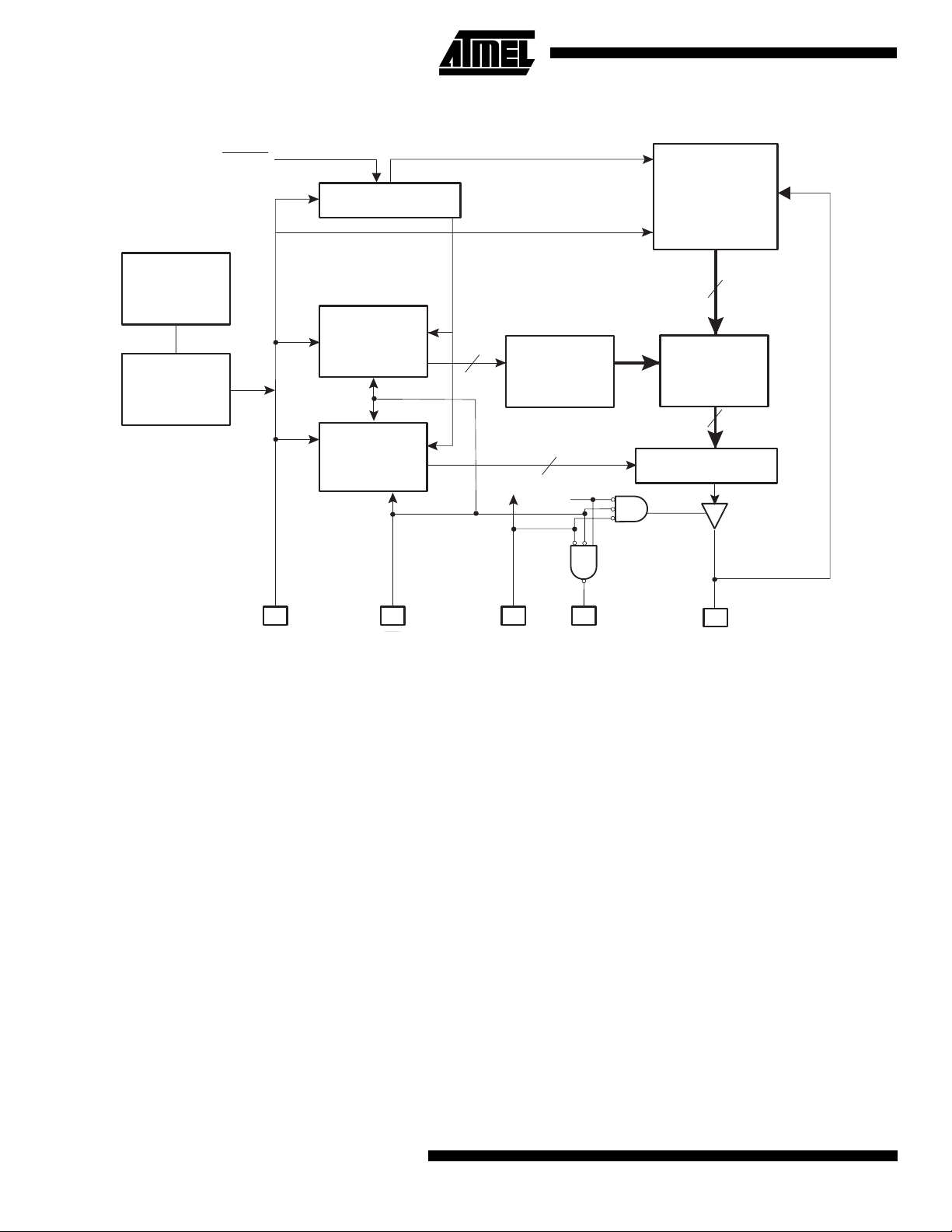
Block Diagram
SER_EN
PROGRAMMING
MODE LOGIC
PROGRAMMING
DATA SHIFT
REGISTER
OSC
CONTROL
ROW
ADDRESS
COUNTER
OSC
BIT
COUNTER
Device Configuration
The control signals for configuration EEPROMs–nCS, OE,
and DCLK–interface directly with the FPGA device control
signals. All FPGA devices can control the entire configuration process and retrieve data from the configuration
EEPROM without requ iring an external intelligent c ontroller.
The configuration EEPROM devi ce’s OE and nCS pins
control the t ri-state buf fer on the DAT A output pin a nd
enable the addres s coun ter and th e os cillato r. W hen OE is
driven low, the configuration EEPROM device resets the
address counter and tri -states its DATA pin. The nCS pin
controls the output of the AT17A Series. If nCS is held high
after the OE reset pulse, the counter is disabled and the
DATA output pin is tri-stated. When nCS is driven low, the
counter and the DATA outp ut pin are enabled. Whe n OE is
driven low again, the address counter is reset and the
DATA output pin is tri-stated, regardless of the state of the
nCS.
When the configurator has driven out all of its data and
nCASC is driven low, the device tri-states the DATA pin to
avoid contention with other configurators. Upon power-up,
the address counter is automatically reset.
24/32
11
ROW
DECODER
5
TC
nCSDCLK OE nCASC DATA
EEPROM
CELL
MATRIX
COLUMN
DECODER
24/32
FPGA Device Configuration
FPGA devices can be configured with an AT17A Series
EEPROM. The AT17A Series device stores configuration
data in its EEPROM array and clocks the data out serially
with its internal oscil lator. The OE, nCS , and DCLK pins
supply the control signals for the address counter and the
output tri-state buffer. The AT17A Series device sends a
serial bitstream of configuration data to its DATA pin, which
is connected to the DATA0 input pin on the FPGA device.
When configuration data for a FPGA device exceeds the
capacity of a single AT17A Series device, multiple AT17A
Series devices can be serially linked togethe r. When multiple AT17A Ser ies dev ices are requir ed, the nCA SC and
nCS pins prov ide han dsha king betwee n the A T17A S erie s
devices.
The position of an AT17A Series device in a chain determines its operation. The first AT17A Ser ies device in a
Configurator chain is powered up or reset with nCS low and
is configured for FPGA devic es protocol. Th is AT17A
Series device supplies all clock pulses to one or more
FPGA devices and to any downstream AT17A Series during configuration. T he first AT 17A Ser ies device also pro vides the first stream of data to the FPGA devices during
2
AT17C/LV/512A/010A
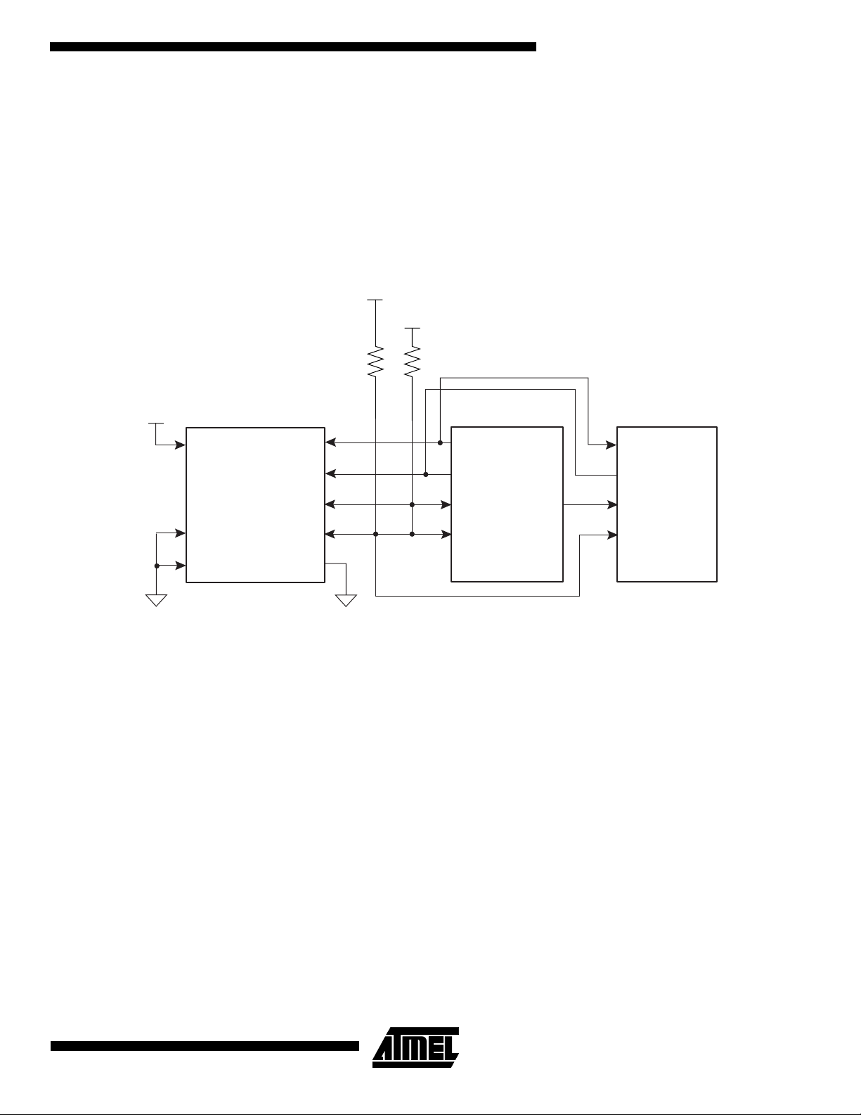
AT17C/LV/512A/010A
multi-device configuration. Once the first AT17A Series
device finish es sending c onfiguration data, it dri ves its
nCASC pin low, whi ch drives the nCS pin of the second
AT17A Series device low. This activates the second AT17A
Series device to send configu ration data to the FPGA
device.
The first AT17A Series device clocks all subsequent AT17A
Series devices until configuration is complete. Once all
AT17A Series device is driven high by CONF_DONE on
the FPGA devices, the first AT17A Se ries dev ice clock s 16
additional cycles to initialize the FPGA device. Then the
first AT17A Series device goes int o ze ro -power (id le) st ate.
If nCS on the first AT17A Series device is driven high
before all configuration data is transferred–or if the nCS is
not driven high after all configuration data is transferred–
the nSTATUS is driven low, indicating a configuration error.
configuration data is transferred and nCS on the first
Figure 1. FPGA Device Configured with Two AT17A Series Devices
VCC
VCC
1KW 1KW
VCC
nCONFIG
Device 1
DATA0
CONF_DONE
DCLK
DCLK
DATA
AT17C010A
Device 1
nCASCnCS
AT17C010A
Device 2
DCLK
DATA
nCS
nSTATUSMSEL0
nCEMSEL1
GND GND
OE
OE
3
Pin Configurations
Pin Number
(20-Pin PLCC) Pin Name Pin Type Description
2 DATA Output Serial data output.
4 DCLK I/O Clock output or clock input. Rising edges on DCLK increment the internal address
counter and present the next bit of data to the DATA pin. The counter is incremented
only if the OE input is held high, the nCS input is held low, and all configuration data
has not been transferred to the target device (otherwise, in FPGA 10K master mode,
the DCLK pin drives low).
5 WP1 Input WRITE PROTECT (1). Used to protect portions of memory during programming. See
programming guide for details.
8 RESET
9 nCS Input Chip select input (active low). A low input allows DCLK to increment the address
10 GND Ground A 0.2 µF decoupling capacitor should be placed between the V
12 nCASC Output Cascade select output (active low). This output goes low when the address counter
15 READY Output Open c ollector reset state indica tor . Driven Low during po wer-up reset, re leased wh en
18 SER_EN
20 V
/OE Input Output enable (ac tiv e h igh) and reset (acti v e lo w) . A lo w logic l e v e l resets the addres s
counter. A high logic level enables DATA and permits the address counter to count. In
the mode, if this pin is low (reset), the internal oscillator becomes inactive and DCLK
drives low.
counter and enables DATA to drive out. If the AT17A Series is reset with nCS low, the
device initializes as the first device in a daisy-chain. If the AT17A Series is reset with
nCS high, the device initializes as the next AT17A Series device in the chain
and GND pins.
CC
has reached its maximum value. In a daisy-chain of AT17A Series devices, the
nCASC pin of one device is usually connected to the nCS input pin of the next device
in the chain, which permits DCLK to clock data from the next AT17A Series device in
the chain.
A2 Input Device selection input, A2. This is used to enable (or select) the device during
is Low (see Programming Guide for more details)
CC
programming, when SER_EN
power-up is complete. (Recommend a 4.7KΩ Pull-up on this pin if used).
Input Serial enable is normally high during FPGA loading operations. Bringing SER_EN
Low, enables the two wire serial interface mode for programming.
Po wer Power pin.
Absolute Maximum Ratings*
Operating Temperature..................................-55°C to +125°C
Storage Temperature.....................................-65°C to +150°C
Voltage on Any Pin
with Respect to Ground.............................-0.1V to VCC + 0.5V
Supply Voltage (V
Maximum Soldering Temp. (10 s @ 1/16 in.)..................260°C
ESD (R
4
= 1.5K, C
ZAP
AT17C/LV/512A/010A
) .........................................-0.5V to +7.0V
CC
= 100 pF)................................ 2000V
ZAP
*NOTICE: Stresses beyond those listed under Absolute Maxi-
mum Ratings may cause permanent damage to the
device. These are stress ratings only, and functional
operation of the device at these or any other conditions beyond those listed under Operating Cond iti ons
is not implied. Exposure to Absolute Maximum Ratings conditions for extended periods of time may
affect device reliability.

Operating Conditions
AT17C/LV/512A/010A
AT17CXXXA AT17LVXXXA
Symbol Description
Commercial
V
CC
Industrial
Military
Supply voltage relative to GND
-0°C to +70°C
Supply voltage relative to GND
-40°C to +85°C
Supply voltage relative to GND
-55°C to +125°C
UnitsMin Max Min Max
4.75 5.25 3.0 3.6 V
4.5 5.5 3.0 3.6 V
4.5 5.5 3.0 3.6 V
5

DC Characteristics
V
= 5V ± 5% Commercial / 5V ± 10% Ind./Mil.
CC
Symbol Description Min Max Units
V
V
V
V
V
V
V
V
I
I
IH
IL
OH
OL
OH
OL
OH
OL
CCA
L
High-level input voltage 2.0 V
CC
Low-level input voltage 0 0.8 V
High-level output voltage (IOH = -4 mA)
3.7 V
Commercial
Low-le vel output vo lta ge (IOL = +4 mA) 0.32 V
High-level output voltage (IOH = -4 mA)
3.6 V
Industrial
Low-le vel output vo lta ge (IOL = +4 mA) 0.37 V
High-level output voltage (IOH = -4 mA)
3.5 V
Military
Low-le vel output vo lta ge (IOL = +4 mA) 0.4 V
Supply current, active mode 10 mA
Input or output leakage current (VIN = VCC or GND) -10 10
Commercial 150
I
CCS
Supply current, standby mode AT17010A/512A
Industrial/Military 150
DC Characteristics
VCC = 3.3V ± 10%
V
A
µ
A
µ
A
µ
Symbol Description Min Max Units
V
V
V
V
V
V
V
V
I
I
I
IH
IL
OH
OL
OH
OL
OH
OL
CCA
L
CCS
High-level input voltage 2.0 V
CC
Low-level input voltage 0 0.8 V
High-level output voltage (IOH = -2.5 mA)
2.4 V
Commercial
Low-le vel output vo lta ge (IOL = +3 mA) 0.4 V
High-level output voltage (IOH = -2 mA)
2.4 V
Industrial
Low-le vel output vo lta ge (IOL = +3 mA) 0.4 V
High-level output voltage (IOH = -2 mA)
2.4 V
Military
Low-le vel output vo lta ge (IOL = +2.5 mA) 0.4 V
Supply current, active mode 5 mA
Input or output leakage current (VIN = VCC or GND) -10 10
Commercial 50
Supply current, standby mode
Industrial/Military 50
V
A
µ
A
µ
A
µ
6
AT17C/LV/512A/010A

AC Characteristics
AC Characteristics When Cascading
AT17C/LV/512A/010A
7

.
AC Characteristics for AT17C010A/512A
VCC = 5V ± 5% Commercial / VCC = 5V ± 10% Ind./Mil
Commercial Industrial/Military
Symbol Description
T
T
T
T
T
T
T
T
T
T
F
T
T
V
OE
CE
CAC
OH
DF
LC
HC
SCE
HCE
HOE
MAX
LC
HC
RDY
(2)
(2)
(2)
(2)
(3)
OE to Data Delay 30 35 ns
nCS to Data Delay 45 45 ns
CLK to Data Delay 50 55 ns
Data Hold From nCS, OE, or DCLK 0 0 ns
nCS or OE to Data Float Delay 50 50 ns
CLK Low Time Slave Mode 20 20 ns
CLK High Time Slave Mode 20 20 ns
nCS Setup Time to DCLK (to guarantee proper counting) 20 25 ns
nCS Hold Time to DCLK (to guarantee proper counting) 0 0 ns
OE High Time (Guarante es Counter Is Reset) 20 20 ns
MAX Input Clock Frequency Slave Mode 15 15 MHz
CLK Low Time Master Mode 30 250 30 250 ns
CLK High Time Master Mode 30 250 30 250 ns
Ready Pin Open Collector Voltage 1.2 2.4 1.2 2.4 V
AC Characteristics for AT17C010A/512A When Cascading
VCC = 5V ± 5% Commercial / VCC = 5V ± 10% Ind./Mil.
UnitsMin Max Min Max
Symbol Description
(3)
T
T
T
T
CDF
OCK
OCE
OOE
(2)
(2)
(2)
DCLK to Data Float Delay 50 50 ns
DCLK to nCASC Delay 35 40 ns
CE to nCASC Delay 35 35 ns
OE to nCASC Delay 30 30 ns
Notes: 1. Preliminary specifications for military operating range only.
2. AC test load = 50 pF.
3. Float delays are measured with 5 pF AC loads. Transition is measured ± 200 mV from steady state active levels.
Commercial Industrial/Military
UnitsMin Max Min Max
8
AT17C/LV/512A/010A

.
AC Characteristics for AT17C010A/512A
VCC = 3.3V ± 10% Commercial / VCC = 3.3V ± 10% Ind./Mil
Symbol Description
T
T
T
T
T
T
T
T
T
T
F
T
T
V
OE
CE
CAC
OH
DF
LC
HC
SCE
HCE
HOE
MAX
LC
HC
RDY
(2)
(2)
(2)
(2)
(3)
(4)
OE to Data Delay 50 55 ns
nCS to Data Delay 55 60 ns
CLK to Data Delay 60 65 ns
Data Hold From nCS, OE, or DCLK 0 0 n s
nCS or OE to Data Float Delay 50 50 ns
CLK Low Time Slave Mode 25 25 ns
CLK High Time Slave Mode 25 25 ns
nCS Setup Time to DCLK (to guarantee proper counting) 35 40 ns
nCS Hold Time to DCLK (to guarantee proper counting) 0 0 ns
OE High Time (Guarantees Counter Is Reset) 20 20 ns
MAX Input Clock Frequency Slave Mode 15 10 MHz
CLK Low Time Master Mode 30 300 30 300 ns
CLK High Time Master Mode 30 300 30 300 ns
Ready Pin Ope n Collector Voltage 1.2 2.4 1.2 2.4 V
AT17C/LV/512A/0
Commercial Industrial/Military
UnitsMin Max Min Max
AC Characteristics for AT17C010A/512A When Cascading
VCC = 3.3V ± 10% Commercial / VCC =3.3V ± 10% Ind./Mil.
Commercial Industrial/Military
Symbol Description
(3)
T
CDF
(2)
T
OCK
(2)
T
OCE
(2)
T
OOE
Notes: 1. Preliminary specifications for military operating range only.
2. AC test load = 50 pF.
3. Float delays are measured with 5 pF AC loads. Transition is measured ± 200 mV from steady state active levels.
4. Duri ng cascade F
DCLK to Data Float Delay 50 50 ns
DCLK to nCASC Delay 50 55 ns
CE to nCASC Delay 35 40 ns
OE to nCASC Delay 35 35 ns
= 12.5 MHz
MAX
UnitsMin Max Min Max
9

Ordering Information - 5V Devices
Memory
Size (K) Ordering Code Package Operation Range
512K
1M Bit
(1)
(2)
AT17C512A-10JC 20J Commercial
(0°C to 70°C)
AT17C512A-10JI 20J Industrial
(-40°C to 85°C)
AT17C010A-10JC 20J Commercial
(0°C to 70°C)
AT17C010A-10JI 20J Industrial
(-40°C to 85°C)
Ordering Information - 3.3V Devices
Memory
Size (K) Ordering Code Package Operation Range
(1)
512K
(2)
1M Bit
Notes: 1. Use 512K density parts to replace Altera EPC1441.
2. Use 1M density parts to replace Altera EPC1
AT17LV512A-10JC 20J Commercial
(0°C to 70°C)
AT17LV512A-10JI 20J Industrial
(-40°C to 85°C)
AT17LV010A-10JC 20J Commercial
(0°C to 70°C)
AT17LV010A-10JI 20J Industrial
(-40°C to 85°C)
10
20J
Package Type
20-Lead, Plastic J-Leaded Chip Carrier (PLCC)
AT17C/LV/512A/010A

Packaging Information
20J, 20-Lead, Plastic J-Leaded Chip Carrier (PLCC)
Dimensions in Inches and (Millimeters)
JEDEC STANDARD MS-018 AA
AT17C/LV/512A/0
11
 Loading...