

ATMEL AT17LV512-10JI, AT17LV512-10JC, AT17C010-10JI, AT17C010-10JC, AT17LV010-10JI Datasheet
...
Features
•
E2 Programmable 524, 288 x 1 and 1,04 8,5 76 x 1 bit Serial Memories Designe d To Store
Configuration Programs For Field Programmable Gate Arrays (FPGA)
•
Simple Interface to SRAM FPGAs
•
Compatible With Atmel AT6000, AT40K FPGAs, Altera EPF8K, EPF10K,
EPF6K FPGAs, ORCA FPGAs, Xilinx XC3000, XC4000, XC5200 FPGAs, Motorola
MPA1000 FPGAs
•
Cascadable To Support Additional Configurations or Future Higher-density Arrays
•
Low-power CMOS EEPROM Process
•
Programmable Reset Polarity
•
Available In PLCC Package (Pin Compatable across Product Family)
•
In-System Programmable Via 2-Wire Bus
•
Emulation of 24CXX Serial EPROMs
•
Available in 3.3V ± 10% LV and 5V Versions
•
System Friendly READY Pin
FPGA
Configuration
2
E
PROM
Description
The AT17C512/010 and AT17LV512/010 (high-density AT17 Series) FPGA Configuration EEPROMs (Configurators) provide an easy-to-use, cost-effective configuration
memory for Field Program mable Gate Arrays. The high -densit y AT17 Series is packaged in the popular 20-pin PLCC. The hig h-densi ty AT17 S eries fam ily uses a simple
serial-access procedure to configure one or more FPGA devices. The high-density
AT17 Series organization supplies enou gh memory to configure one or multi ple
smaller FPGAs. The user can select the polarity of the reset function by programming
one EEPROM byte. The devices also support a write protection mode and a system
friendly READY pin, which signifies a “good” power level to the device and can be
used to ensure reliable system power-up.
The high-density AT17 Series can be program med with industry-standar d programmers, and the Atmel ATDH2200 Programming board.
Pin Configurations
20-Pin PLCC
CLK
WP1
D
A
T
N
A
C
3 2 1 20 19
4
V
C
N
C
N
C
C
NC
18
SER_EN
17
Memory
512K and 1M
AT17C512
AT17LV512
AT17C010
AT17LV010
RESET/OE
WP2
CE
9510611712813
N
G
N
C
N
D
NCN
C
C
16
15
14
NC
READY
CEO
Rev. 0944A-A–12/97
1
Controlling The High-Density AT17 Series Serial EEPROMs
Most connections between the FPGA device and the Serial
EEPROM are simple and self-explanatory:
• The DATA output of th e high-density AT17 Series dr ives
DIN of the FPGA devices.
• The master FPGA CCLK output dr ives the CLK input of
the high-density AT17 Series.
• The CEO
input of the next AT17C/LV512 /010 in a ca scad e chain of
PROMs.
•SER_EN
ISP).
READY is available as an open-collector indicator of the
device’s RESET s tatus; i t is driven L ow while the device is
in its POWER-ON RESET cycle and released (tri-stated)
when the cycle is complete.
There are two different wa ys to use the inp uts CE
as shown in the AC Characteristics waveforms.
output of any AT17C/LV5 12/010 drives the CE
must be connected to VCC, (except during
and OE,
Condition 1
The simplest connection is to have the FPGA D/P output
drive both CE
and RESET/OE in paral le l ( F ig ure 1) . Du e to
its simplicity, however, this method will fail if the FPGA
receives an external reset condi tion during the configuration cycle. If a sy stem rese t is ap plied to the FPGA, it will
abort the original configuration and then reset itself for a
new configuration, as in tend ed. O f cour s e, the hig h-density
AT17 Series does not see the ex ter nal r es et sig nal an d wi ll
not reset its internal address counters and, consequently,
will remain out of sync with the FPGA for the remainder of
the configuration cycle.
Condition 2
The FPGA D/P output drives only the CE in put of t he high density AT17 Series, while its OE
inversion of the input to the FPGA RESET
connection works under all normal circumstances, even
when the user aborts a configuration before D/P
High. A High level on the RESET/OE
AT17C/LVxxx – during FPGA reset – cl ears t he Conf igu rator’s internal address pointer, so that the reconfiguration
starts at the beginn ing . The high- de ns ity AT 17 Ser ies do es
not require an inverter since the RESET polarity is programmable.
input is driven by the
input pin. This
has gone
input to the
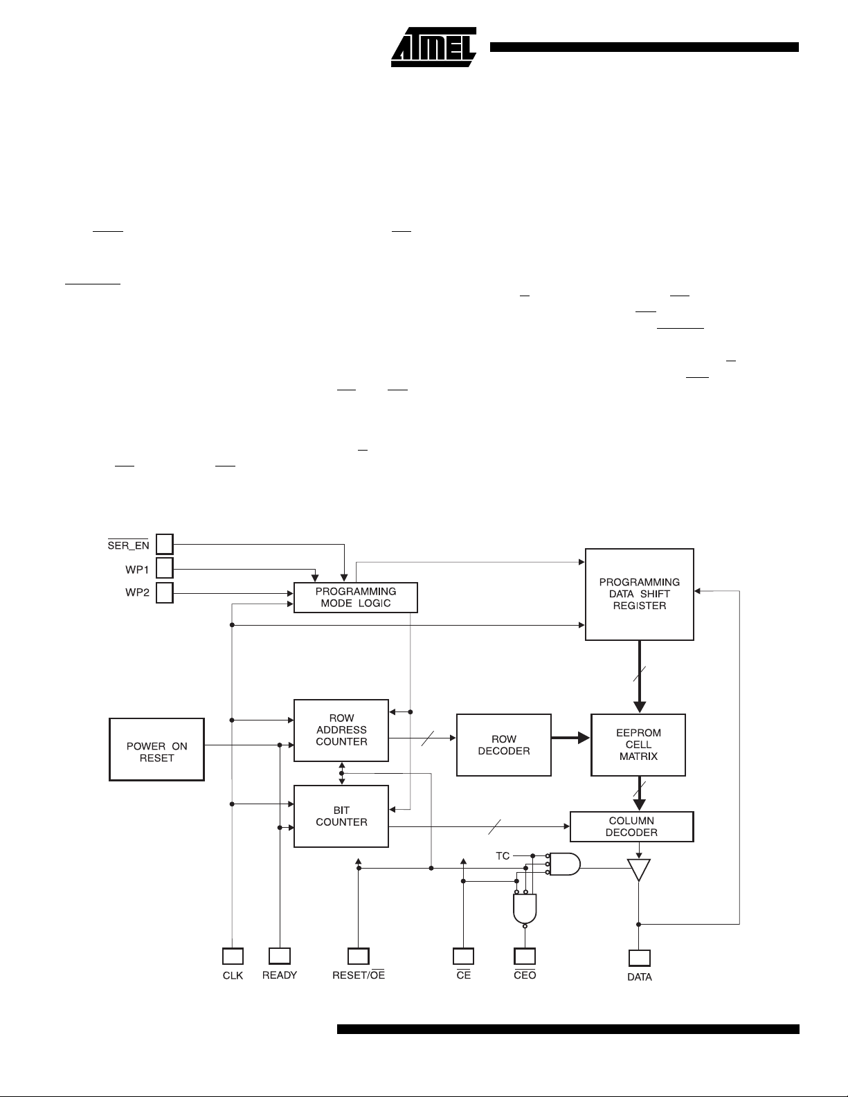
Block Diagram
2
AT17C/LV512/010
AT17C/LV512/010
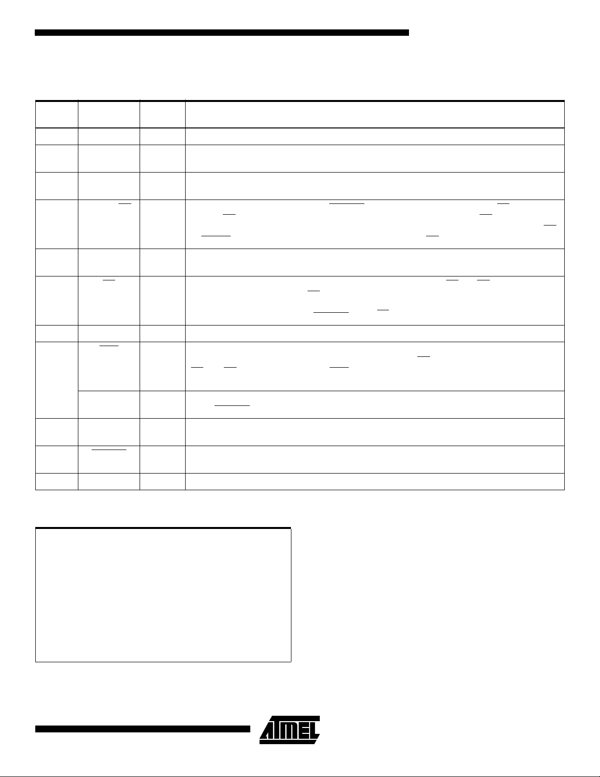
Pin Configurations
20
PLCC Name I/O Description
2 DATA I/O Three-state DATA output for reading. Input/Output pin for programming.
4 CLK I Clock input. Used to increment the internal address and bit counter for reading and
programming.
5 WP1 I WRITE PROTECT (1). Used to protect portions of memory during programming. See
programming guide for details.
6 RESET/OE
7 WP2 I WRITE PROTECT (2). Used to protect portions of memory during programming. See
I RESET/Output Enable input (when SER_EN is High). A Low level on both the CE and
RESET/OE
address and bit counters . The l ogic p olarity of t his input i s prog ra mmab l e as eithe r RESET/ OE
or RESET
programming guide for details.
inputs enables the data output driver. A High level on RESET/OE resets both the
/OE. This document describes the pin as RESET/OE.
8CE
10 GND Ground pin.
14 CEO
A2 I Device selection input, A2. This is used to enable (or select) the device during programming,
15 READY O Open collector reset state indicator. Driven Low during power-up reset, released when power-
17 SER_EN I Serial enable is normally high during FPGA loading operations. Bringing SER_EN Low,
20 V
CC
I Chip Enable input. Used for device selection. A Low level on both CE and OE enables the data
output driver. A High level on CE
device into a low power mode. Note this pin will not
Programming mode (i.e., when SER_EN
O Chip Enable Out output. This signal is asserted Low on the clock cycle following the last bit
read from the memory. It will stay Low as long as CE and OE
CE
until OE goes Hig h. There after, CEO will stay Hig h until the ent ire PR OM is read again and
senses the status of RESET polarity.
when SER_EN
up is complete. (Recommend a 4.7KΩ Pull-up on this pin if used).
enables the two wire serial interface mode for programming.
+3.3V/+5V power supply pin.
is Low (see Programming Guide for more details)
disables both the address and bit counters and forces the
enable/disable the device in 2-wire Serial
is Low).
are both Low. It will then follow
Absolute Maximum Ratings*
Operating Temperature.................................. -55°C to +125°C
Storage Temperature.....................................-65°C to +150°C
Voltage on Any Pin
with Respect to Ground............................-0.1V to V
Supply Voltage (V
).........................................-0.5V to +7.0V
CC
+ 0.5V
CC
*NOTICE: Stresses beyond those listed under Absolute Maxi-
mum Ratings may cause permanent damage to the
device. These are stress ratings only, and functional
operation of the device at these or any other conditions beyond those listed under Operating Cond itions
is not implied. Exposure to Absolute Maximum Ratings conditions for extended periods of time may
affect device reliability.
Maximum Soldering Temp. (10 s @ 1/16 in.)..................260°C
ESD (R
= 1.5K, C
ZAP
= 100 pF)...............................2000V
ZAP
3

FPGA Master Serial Mode Summary
The I/O and logic functions of the FPGA and thei r associated interconnections are establish ed by a configuration
program. The program is loaded either automatically upon
power up, or on command, depending on the state of the
three FPGA m ode pi ns. In Mast er Mode , the F PGA a utomatically loads the configuration program from an external
memory. The Serial Configuration EEPROM has been
designed for compatibility with the Master Serial Mode.
Cascading Serial Configuration
EEPROMs
For multiple FPGAs configured as a daisy- chain, or for
future FPGAs requiring larger configuration memories, cascaded Configurators provide additional memory.
As the last bit from the first Configurator is read, the clock
signal to the Configurator asserts its CEO
disables its DATA line. The second Configurator recognizes the Low level on its CE
output.
Figure 1.
Condition 1 Connection
input and enables its DAT A
output Low and
After configu ratio n is comp lete, the addr ess co unters o f all
cascaded Configurators are reset if the reset signal drives
the RESET/OE
level.
If the address counters are not to be reset upon completion, then the RESET/O E
more details, please reference the AT17C Series Programming Guide.
on each Configurator to it s active (High)
inputs can be tied to ground. For
Programming Mode
The programming mode i s entered by b ringing SER_EN
Low. In this mode the chip can be programmed by the 2wire interface. The programming is done at V
only. Programming super voltages are generated inside the
chip. See the Programming Specification for Atmel's Configuration Memories Application Note for further information. The AT17C Series parts ar e read/wri te at 5V nom inal.
The AT17LV parts are read/write at 3.3V nominal.
supply
CC
AT17C/ LVXXX Res et Polarity
The AT17C/LVXXX lets the user choose the reset polarity
as either RESET/OE
or RESET/OE.
Operating Conditions
Symbol Description
Commercial
V
CC
Industrial
Military
Supply voltage relative to GND
-0°C to +70°C
Supply voltage relative to GND
-40°C to +85°C
Supply voltage relative to GND
-55°C to +125°C
Standby Mode
The AT17C/LVXXX enters a low-power standby mode
whenever CE
tor consumes less than 0.5mA at 5.0 volts. The output
remains in a high impedance state regardless of the state
of the OE
is asserted High. In this mode, the Configura-
input.
AT17CXXX AT17LVXXX
UnitsMin/Max Min/Max
4.75 / 5.25 3.0 / 3.6 V
4.5 / 5.5 3.0 / 3.6 V
4.5 / 5.5 3.0 / 3.6 V
4
AT17C/LV512/010

AT17C/LV512/010
DC Characteristics
V
= 5V ± 5% Commercial / 5V ± 10% Ind./Mil.
CC
Symbol Description Min Max Units
V
V
V
V
V
V
V
V
I
CCA
I
L
I
CCS
IH
IL
OH
OL
OH
OL
OH
OL
High-level input voltage 2.0 V
CC
Low-level input voltage 0 0.8 V
High-level output voltage (IOH = -4 mA)
3.86 V
Commercial
Low-le vel output voltage (IOL = +4 mA) 0.32 V
High-level output voltage (IOH = -4 mA)
3.76 V
Industrial
Low-le vel output voltage (IOL = +4 mA) 0.37 V
High-level output voltage (IOH = -4 mA)
3.7 V
Military
Low-le vel output voltage (IOL = +4 mA) 0.4 V
Supply current, active mode (at FMAX) 10 mA
Input or output leakage current (VIN = VCC or GND) -10 10
Commercial 0.5 mA
Supply current, standby mode
Industrial/Military 0.5 mA
V
A
µ
DC Characteristics
VCC = 3.3V ± 10%
Symbol Description Min Max Units
V
V
V
V
V
V
V
V
I
CCA
I
L
I
CCS
IH
IL
OH
OL
OH
OL
OH
OL
High-level input voltage 2.0 V
CC
Low-level input voltage 0 0.8 V
High-level output voltage (IOH = -2.5 mA)
2.4 V
Commercial
Low-le vel output voltage (IOL = +3 mA) 0.4 V
High-level output voltage (IOH = -2 mA)
2.4 V
Industrial
Low-le vel output voltage (IOL = +3 mA) 0.4 V
High-level output voltage (IOH = -2 mA)
2.4 V
Military
Low-le vel output voltage (IOL = +2.5 mA) 0.4 V
Supply current, active mode 5 mA
Input or output leakage current (VIN = VCC or GND) -10 10
Commercial 100
Supply current, standby mode
Industrial/Military 100
V
A
µ
A
µ
A
µ
5

AC Characteristics
AC Characteristics When Cascading
6
AT17C/LV512/010

.
AC Characteristics for AT17C512/010
VCC = 5V ± 5% Commercial / VCC = 5V ± 10% Ind./Mil
Symbol Description
(2)
T
T
T
T
T
T
T
T
T
T
F
V
OE
CE
CAC
OH
DF
LC
HC
SCE
HCE
HOE
MAX
RDY
(2)
(2)
(2)
(3)
OE to Data Delay 30 35 ns
CE to Data Delay 45 45 ns
CLK to Data Delay 50 50 ns
Data Hold From CE, OE, or CLK 0 0 ns
CE or OE to Data Float Delay 50 50 ns
CLK Low Time 20 20 ns
CLK High Time 20 20 ns
CE Setup Time to CLK (to guara ntee prop er coun ting) 20 25 ns
CE Hold Time to CLK (to guarantee proper counting) 0 0 ns
OE High Time (Guarantees Counter Is Reset) 20 20 ns
MAX Input Clock Frequency 15 15 MHz
Ready Pin Ope n Collector Voltage 1.2 2.2 1.2 2.2 V
AT17C/LV512/010
Commercial/Industrial Military
UnitsMin Max Min Max
AC Characteristics for AT17C512/010 When Cascading
VCC = 5V± 5% Commercial / VCC = 5V ± 10% Ind./Mil.
Commercial/Industrial Military
Symbol Description
(3)
T
CDF
(2)
T
OCK
(2)
T
OCE
(2)
T
OOE
Notes: 1. Preliminary specifications for military operating range only.
2. AC test load = 50 pF.
3. Float delays are measured with 5 pF AC loads. Transition is measured ± 200 mV from steady state active levels.
CLK to Data Float Delay 50 50 ns
CLK to CEO Delay 35 40 ns
CE to CEO Delay 35 35 ns
RESET/OE to CEO Delay 30 30 ns
UnitsMinMaxMinMax
7

AC Characteristics for AT17LV512/010
VCC = 3.3V ± 10%
Symbol Description
(2)
T
OE
T
CE
T
CAC
T
OH
T
DF
T
LC
T
HC
T
SCE
T
HCE
T
HOE
F
MAX
V
RDY
Notes: 1. Preliminary specifications for military operating range only.
OE to Data Delay 50 55 ns
(2)
CE to Data Delay 55 60 ns
(2)
CLK to Data Delay 55 60 ns
Data Hold From CE, OE, or CLK 0 0 ns
(3)
CE or OE to Data Float Delay 50 50 ns
CLK Low Time 25 25 ns
CLK High Time 25 25 ns
CE Setup Time to CLK (to guarantee proper counting) 30 35 ns
CE Hold Time to CLK (to guarantee proper counting) 0 0 ns
OE High Time (Guarantees Counter Is Reset) 25 25 ns
(4)
MAX Input Clock Frequency 15 10 MHz
Ready Pin Open Collector Voltage 1.2 2.2 1.2 2.2 V
2. AC test load = 50 pF.
3. Float delays are measured with 5 pF AC loads. Transition is measured ± 200 mV from steady state active levels.
4. During cascade F
= 12.5 MHz.
MAX
Commercial/Industrial Military
Min Max Min Max
Units
AC Characteristics for AT17LV512/010 When Cascading
VCC = 3.3V ± 10%
Commercial/Industrial Military
Symbol Description
(3)
T
CDF
(2)
T
OCK
(2)
T
OCE
(2)
T
OOE
CLK to Data Float Delay 50 50 ns
CLK to CEO Delay 50 55 ns
CE to CEO Delay 35 40 ns
RESET/OE to CEO Delay 35 35 ns
UnitsMinMaxMinMax
8
AT17C/LV512/010

AT17C/LV512/010
Ordering Information - 5V Devices
Memory Size Ordering Code Package Operation Range
512K AT17C512-10JC 20J Commercial
(0°C to 70°C)
AT17C512-10JI 20J Industrial
(-40°C to 85°C)
1M AT17C010-10JC 20J Commercial
(0°C to 70°C)
AT17C010-10JI 20J Industrial
(-40°C to 85°C)
Ordering Information - 3.3V Devices
Memory Size Ordering Code Package Operation Range
512K AT17LV512-10JC 20J Commercial
(0°C to 70°C)
AT17LV512-10JI 20J Industrial
(-40°C to 85°C)
1M AT17LV010-10JC 20J Commercial
(0°C to 70°C)
AT17LV010-10JI 20J Industrial
(-40°C to 85°C)
Package Type
20J 20 Lead, Plastic J-Leaded Chip Carrier (PLCC)
9
 Loading...