

ATMEL AT17C128A-10JI, AT17C128A-10JC, AT17LV256A-10JI, AT17LV256A-10JC, AT17LV128A-10JI Datasheet
...
1
Features
•
EE Programmab le 65,536 x 1, 131,0 72 x 1 and 262,1 44 x 1 bit Serial M emories De signed
to Store Configuration Programs for Programmable Gate Arrays
•
Simple Interface to SRAM FPGAs Requires Only One User I/O Pin
•
Able to Configure with EPF6000 and EPF8000, Flex 10K FPGAs
•
Cascadable To Support Additional Configurations or Future Higher-Density Arrays
(17C128/256 only)
•
Low-Power CMOS EEPROM Process
•
Programmable Reset Polarity
•
Available in Industry-Standard Pin-Compatible PLCC Package
•
In-System Programmable via 2-Wire Bus
•
Emulation of 24CXX Serial EEPROMs
•
Available in 3.3V and 5V Versions
Description
The AT17C65/128/256A and AT17LV65/128/256A (AT17A Series) FPGA Configuration EEPROMS (Configurator) provide an easy-to-use, cost-effective configuration
memory for Field Programmable Gate Arrays. The AT17A Series is packaged in the
popular 20-pin PLCC. The AT17 A Series family uses a sim ple s erial-ac cess p rovide s
to configure one or more FPGA devices. The AT17A Series organization suppli es
enough memory t o confi gure one or multipl e smal ler FPGA s. Using a speci al featu re
of the AT17A Series, the user can select the polarity of the reset function by programming a special EEPROM bit.
The AT17A Series is pin compatible with the industry standard configurator, and can
be programmed with industry standard programmers.
Pin Configurations
20-Pin PLCC
4
5
6
7
8
18
17
16
15
14
CLK (DCLK)
NC
NC
NC
RESET/OE (RESET/OE)
SER_EN
NC
NC
NC
NC
321
20
19
910111213
CE (nCS)
GND
NC
CEO (nCASC)
NC
NC
DATANCVCC
NC
Rev. 0996A–07/98
FPGA
Configuration
EEPROM
65K, 128K and 256K
AT17CxxxA
AT17LVxxxA
AT17A Series
2
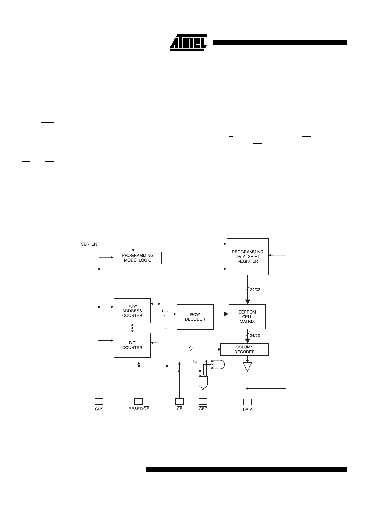
Controlling The AT17A Series Serial EEPROMs
Most connections betwe en the FPG A devic e and the s erial
EEPROM are simple and self-explanatory.
• The DATA output of the AT17A Se ries drives DIN of the
FPGA devices.
• The master FPGA CCLK output dr ives the CLK inpu t of
the AT17A Series.
• The CEO
output of any AT17C/LV128/256A drives the
CE
input of the next AT17C/LV65/128/256 in a cascade
chain of PROMs.
•SER_EN
must be connected to VCC.
There are, however, two different ways to use the inputs
CE
and OE, as shown in the AC Characteristics wave-
forms.
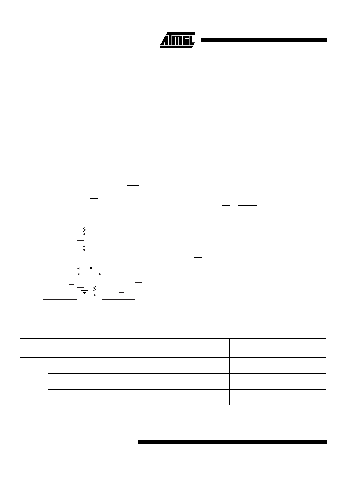
Condition 1
The simplest connection is to have the FPGA D/P output
drive both CE
and RESET/OE in parall el (Fi gur e 1 ). Due to
its simplicity, however, this method will fail if the FPGA
receives an external rese t cond ition d uring the c onfigur a-
tion cycle. If a system reset is applied to the F PGA, it will
abort the original configuration and then reset itself for a
new configuration, as intended. Of course, the AT17A
Series does not s ee the exte rnal reset s ignal and wi ll not
reset its internal address co unters and, co nsequently, wil l
remain out of sync with the FPGA for the remainder of the
configuration cycle.
Condition 2
The FPGA D/P output drives only the CE input of the
AT17A Series, wh ile its OE
input is driven by the inve rsion
of the input to the FP G A RES ET
input pin. This conn ec tio n
works under all nor mal cir cums ta nce s, ev en when the us er
aborts a configuration before D/P
has gone high. A hig h
level on the RESET/OE
input to the AT17C/LVxxxA – during FPGA reset – clears the Configurator's internal address
pointer, so that the reconfiguration starts at the beginning.
The AT17A Series does not require an inverter since the
RESET polarity is programmable.
Block Diagram
AT17A Series
3
Pin Configurations
PLCC/S
OIC DIP
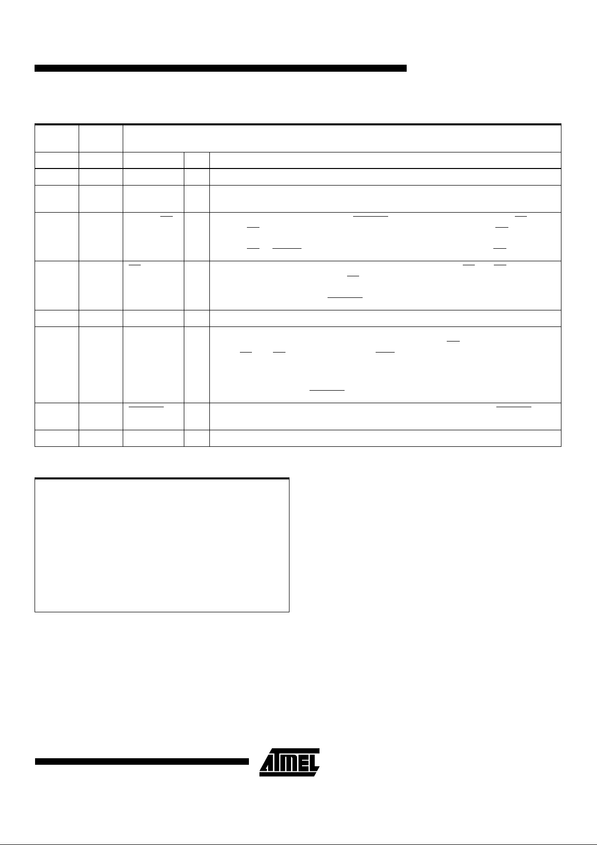
Pin Pin Name I/O Description
2 1 DATA I/O Three-state DATA output for reading. Input/Output pin for programming.
4 2 CLK I Clock input. Used to increment the internal address and bit counter for reading and
programming.
8 3 RESET/OE RESET/Output Enable input (when SER_EN is High). A low level on both the CE and
RESET/OE
inputs enab les the da ta ou tput driv er. A h igh level on RESET /OE rese ts bo th
the address and bit counters. A logic polarity of this input is programmable as either
RESET/OE or RESET/OE. This document describes the pin as RESET/OE.
94CE
I Chip Enable input. Used for device selection. A low level on both CE and OE enables the
data output driver. A high level on CE
disables both the address and bit counters and
forces te device into a low-power mode. Note this pin will not enable/disable the device in
2-wire serial mode (ie; when SER_EN is low).
10 5 GND Ground pin
12 6 CEO O Chip Enable Out output. This signal is asserted low on the clock cycle following the last
bit read from the memory. It will stay low as long as CE and OE are both low. It will then
follow CE
until OE goes high. Thereafter, CEO will stay high until the entire PROM is
read again and senses the status of RESET polarity.
A2 I Device selection input, A2. This is used to enable (or select) the device during
programming and when SER _EN
is low (see Programming Guide for more details).
18 7 SER_EN I Serial enable is normally high during FPGA loading operations. Bringing SER_EN low,
enables the 2-wire serial interface for programming.
20 8 V
CC
+3.3V/+5V power supply pin.
Absolute Maximum Ratings*
Operating Temperature..................................-55°C to +125°C
*NOTICE: Stresses beyond those listed under “Absolute
Maximum Ratings” may cause permanent damage to the dev ice. Th is is a s tress rating only an d
functional oper ati on of the de vi ce at t hes e o r any
other conditions beyond those indicated in the
operational sections of this specification is not
implied. Exposure to absolute maximum rating
conditions f or e xtended periods ma y af fect dev ice
reliability .
Storage Temperature.....................................-65°C to +150°C
Voltage on Any Pin
with Respect to Ground.............................-0.1V to V
CC +
0.5V
Supply Voltage (V
CC
) .......................................-0.5 V to + 7.0V
Maximum Soldering Temp. (10 sec. @ 1/16 in.).............260°C
ESD (R
ZAP
= 1.5K, C
ZAP
= 100 pF)................................. 2000V
AT17A Series
4
FPGA Master Serial Mode Summary
The I/O and logic functions o f the FPGA and their assoc iated interconnections are established by a configuration
program. The program is loaded either automatically upon
power up, or on command, dependin g on the state of th e
three FPGA mode pi ns. In Master M ode, the FPGA automatically loads the configuration program from an external
memory. The Serial Configuration EEPROM has been
designed for compatibility with the Master Serial Mode.
Cascading Serial Configuration
EEPROMs (AT17C/LV256A)
For multiple FPGAs config ured as a daisy-chain, or for
future FPGAs requiring larger configuration memories, cascaded Configurators provide additional memory
(17C/LV128/256A only).
After the last bit f rom t he first Configurator is rea d, t he next
clock signal to the Configurator asserts its CEO
output Low
and disables its DA TA line . The sec ond Confi gurator r ecognizes the low lev el o n i ts CE
input and enables i ts DATA
output.
Figure 1.
Condition 1 Connection
After configuration is complete, the address counters of all
cascaded Configurators are reset if the reset signal drives
the RESET/OE
on each Configurator Active.
If the address counters are not to be reset upon completion, then the RES ET/O E
inputs can be tied to groun d. For
more details, please refere nc e the A T17C S er ies Pr o gramming Guide
Programming Mode
The programming mode is entered by bringing SER_E N
low. In this mode the chip can be program med by the 2wire interface. The programming is done at V
CC
supply
only. Programming super voltages are generated inside the
chip. See the Programming Specification for Atmel’s Configuration Memories Application Note for further information. The AT17C Series parts are rea d/write at 5V nominal .
The AT17LV parts are read/write at 3.0V nominal.
AT17C/LVxxx Reset Polarity
The AT17C/LVxxxA lets the user choose the reset polarity
as either RESET/OE
or RESET/OE.
Standby Mode
The AT17C/LVxxxA enters a low-power standby mode
whenever CE
is asserted high. In this mode, the Configurator consumes less than 1.0 mA of current. The output
remains in a high-impedance state regardless of the state
of the OE
input.
CS
REBOOT
M2
M1
M0
FPGA
D0
CCLK
CON
FLEX DEVICE
SERIAL
EEPROM
DATA
CLK
CE
SER_EN
RESET/OE
AT17CXX
V
CC
FLEX 10K, FLEX 16K
(CLK REQUIRED)
Operating Conditions
Symbol Description
AT17Cxxx AT17LVxxx
UnitsMin/Max Min/Max
V
CC
Commercial Supply voltage relative to GND
-0°C to +70°C
4.75/5.25 3.0/3.6 V
Industrial Supply voltage relative to GND
-40°C to +85C
°
4.5/5.5 3.0/3.6 V
Military Supply voltage relative to GND
-55°C to +125C
4.5/5.5 3.0/3.6 V

AT17A Series
5
.
DC Characteristics
VCC = 5V ± 5% Commercial / 5V ± 10% Ind./Mil.
Symbol Description Min Max Units
V
IH
High-level input voltage 2.0 V
CC
V
V
IL
Low-level input voltage 00.8V
V
OH
High-level output voltage (IOH = -4 mA)
Commercial
3.7 V
V
OL
Low-level output voltage (IOL = +4 mA) 0.32 V
V
OH
High-level output voltage (IOH = -4 mA)
Industrial
3.6 V
V
OL
Low-level output voltage (IOL = +4 mA) 0.37 V
V
OH
High-level output voltage (IOH = -4 mA)
Military
3.5 V
V
OL
Low-level output voltage (IOL = +4 mA) 0.4 V
I
CCA
Supply current, active mode 10 mA
I
L
Input or output leakage current (VIN = VCC or GND) -10 10
µ
A
I
CCS
Supply current, standby mode AT17C256
Commercial 75
µ
A
Industrial/Military 150
µ
A
Supply current, standby mode AT17C128/65
Commercial 1 mA
Industrial/Military 2 mA
DC Characteristics
VCC = 3.3V ± 10%
Symbol Description Min Max Units
V
IH
High-level input voltage 2.0 V
CC
V
V
IL
Low-level input voltage 00.8V
V
OH
High-level output voltage (IOH = -2.5 mA)
Commercial
2.4 V
V
OL
Low-level output voltage (IOL = +3 mA) 0.4 V
V
OH
High-level output voltage (IOH = -2 mA)
Industrial
2.4 V
V
OL
Low-level output voltage (IOL = +3 mA) 0.4 V
V
OH
High-level output voltage (IOH = -2 mA)
Military
2.4 V
V
OL
Low-level output voltage (IOL = +2.5 mA) 0.4 V
I
CCA
Supply current, active mode 5mA
I
L
Input or output leakage current (VIN = VCC or GND) -10 10
µ
A
I
CCS
Supply current, stand by mode
Commercial 50
µ
A
Industrial/Military 100
µ
A

AT17A Series
6
AC Characteristics
AC Characteristics When Cascading

AT17A Series
7
.
.
Notes: 1. Preliminary specifications for military operating range only.
2. AC test load = 50 pf.
3. Float delays are measured with 5 pF AC loads. Transition is measured ±200 mV from steady-state active levels.
AC Characteristics for AT17C256A
VCC = 5V ± 5% Commercial / VCC = 5V ± 10% Ind./Mil
Symbol Description
Commercial Industrial/Military
UnitsMin Max Min Max
t
OE
(2)
OE to Data Delay 25 25 ns
t
CE
(2)
CE to Data Delay 45 45 ns
t
CAC
(2)
CLK to Data Delay 50 55 ns
t
OH
(2)
Data Hold From CE, OE, or CLK 0 0 ns
t
DF
(3)
CE or OE to Data Float Delay 50 50 ns
t
LC
CLK Low Time 20 20 ns
t
HC
CLK High Time 20 20 ns
t
SCE
CE Setup Time to CLK (to guarantee proper counting ) 35 40 ns
t
HCE
CE Hold Time to CLk (to guarantee proper counting) 0 0 ns
t
HOE
OE High Time (guarantees counter is reset) 20 20 ns
F
MAX
MAX Input Clock Frequency 12.5 12.5 MHz
AC Characteristics for AT17C256A When Cascading
VCC = 5V± 5% Commercial / VCC = 5V ± 10% Ind./Mil
Symbol Description
Commercial Industrial/Military
UnitsMin Max Min Max
t
CDF
(3)
CLK to Data Float Delay 50 50 ns
t
OCK
(2)
CLK to CEO Dela y 35 40 ns
t
OCE
(2)
CE to CEO Delay 35 35 ns
t
OOE
(2)
RESET/OE to CEO Delay 30 35 ns

AT17A Series
8
.
.
Notes: 1. Preliminary specifications for military operating range only.
2. AC test load = 50 pf.
3. Float delays are measured with 5 pF AC loads. Transition is measured ±200 mV from steady-state active levels.
4. During cascade F
MAX
= 8 MHz.
AC Characteristics for AT17C65/128A
VCC = 5V ± 5% Commercial / VCC = 5V ± 10% Ind./Mil.
Symbol Description
Commercial Industrial/Military
UnitsMin Max Min Max
t
OE
(2)
OE to Data Delay 110 150 ns
t
CE
(2)
CE to Data Delay 50 50 ns
t
CAC
(2)
CLK to Data Delay 50 55 ns
t
OH
(2)
Data Hold From CE, OE, or CLK 0 0 ns
t
DF
(3)
CE or OE to Data Float Delay 50 50 ns
t
LC
CLK Low Time 30 35 ns
t
HC
CLK High Time 30 35 ns
t
SCE
CE Setup Time to CLK (to guarantee pr oper counting) 45 50 ns
t
HCE
CE Hold Time to CLk (to guarantee proper counting) 0 5 ns
t
HOE
OE High Time (guarantees counter is reset) 50 60 ns
F
MAX
(4)
MAX Input Clock Frequency 10 10 MHz
AC Characteristics for AT17C128/256A When Cascading
VCC = 5V ± 5% Commercial / VCC = 5V ± 10% Ind./Mil.
Symbol Description
Commercial Industrial/Military
UnitsMin Max Min Max
t
CDF
(3)
CLK to Data Float Delay 50 50 ns
t
OCK
(2)
CLK to CEO Dela y 65 75 ns
t
OCE
(2)
CE to CEO Delay 55 60 ns
t
OE
(2)
RESET/OE to CEO Delay 55 55 ns

AT17A Series
9
Notes: 1. Preliminary specifications for military operating range only.
2. AC test lead = 50 pf.
3. Float delays are measured with 5 pF AC loads. Transition is measured ±200 mV from steady-state active levels.
4. During cascade F
MAX
= 8 MHz.
AC Characteristics
VCC = 3.3V ± 10%
Symbol Description
Commercial Industrial/Military
UnitsMin Max Min Max
t
OE
(2)
OE to Data Delay 40 45 ns
t
CE
(2)
CE to Data Delay 60 60 ns
t
CAC
(2)
CLK to Data Delay 75 80 ns
t
OH
(2)
Data Hold From CE, OE, or CLK 0 0 ns
t
DF
(3)
CE or OE to Data Float Delay 55 55 ns
t
LC
CLK Low Time 25 25 ns
t
HC
CLK High Time 25 25 ns
t
SCE
CE Setup Time to CLK (to guarantee proper counting) 35 60 ns
t
HCE
CE Hold Time to CLk (to guarantee proper counting) 0 0 ns
t
HOE
OE High Time (guarantees counter is reset) 25 25 ns
F
MAX
(4)
MAX Input Clock Frequency 10 8 10 MHz
AC Characteristics When Cascading
VCC = 3.3V ± 10%
Symbol Description
Commercial Industrial/Military
UnitsMin Max Min Max
t
CDF
(3)
CLK to Data Float Delay 60 60 ns
t
OCK
(2)
CLK to CEO Dela y 55 60 ns
t
OCE
(2)
CE to CEO Delay 55 60 ns
t
OOE
(2)
RESET/OE to CEO Delay 40 45 ns

AT17A Series
10
Ordering Inf o rmation - 5V Devices
Memory
Size (K) Ordering Code Package Operation Range
64K AT17C65 A-10J C 20J Commercial
(0°C to 70°C)
AT17C65A-10JI 20J Industrial
(-40°C to 85°C)
128K AT17C128A-10JC 20J Commercial
(0°C to 70°C)
AT17C128A-10JI 20J Industrial
(-40°C to 85°C)
256K AT17C256A-10JC 20J Commercial
(0°C to 70°C)
AT17C256A-10JI 20J Industrial
(-40°C to 85°C)
Ordering Information - 3.3V Devices
Memory
Size (K) Ordering Code Package Operation Range
64K AT17LV65A-10JC 20J Commercial
(0°C to 70°C)
AT17LV65A-10JI 20J Industrial
(-40°C to 85°C)
128K AT17LV128A-10JC 20J Commercial
(0°C to 70°C)
AT17LV128A-10JI 20J Industrial
(-40°C to 85°C)
256K AT17LV256A-10JC 20J Commercial
(0°C to 70°C)
AT17LV256A-10JI 20J Industrial
(-40°C to 85°C)
Package Type
20J 20-Lead, Plastic J-Leaded Chip Carrier (PLCC)

AT17A Series
11
Packaging Information
20J,
20-Lead, Plastic J-Leaded Chip Carrier (PLCC)
Dimensions in Inches and (Millimeters)
JEDEC STANDARD MS-018 AA
 Loading...