

Datasheet AT17C256-10PI, AT17C256-10PC, AT17C256-10JI, AT17C256-10JC, AT17C128-10SI Datasheet (ATMEL)
...
Features
•
E2 Programmable 65,536 x 1, 131,072 x 1, and 262,144 x 1 bit Seria l Memories Design ed
To Store Configuration Programs For Programmable Gate Arrays
•
Simple Interface to SRAM FPGAs Requires Only One User I/O Pin
•
Compatible With AT6000 FPGAs, ATT3000 FPGA, EPF8000 FPGAs, ORCA FPGAs,
XC2000, XC3000, XC4000, XC5000 FPGAs, MPA1000
•
Cascadable To Support Additional Configurations or Future Higher-density Arrays
(17C128 and 17C256 only)
•
Low-power CMOS EEPROM Process
•
Programmable Reset Polarity
•
Available In the Space-efficient Plastic DIP or Surface-mount
PLCC and SOIC Packages
•
In-System Programmable Via 2-Wire Bus
•
Emulation of 24CXX Serial EPROMs
•
Available in 3.3V ± 10% LV Version
AT17 Series
FPGA
Configuration
2
E
PROM
Description
The AT17C65/128/256 a nd AT17LV65 /128/256 (AT1 7 Series) FPGA Co nfiguratio n
EEPROMS (Configurator) provide an easy-to-use, cost-effective configuration memory for Field Programmable Gate Arrays. The AT17 Series is pack aged in the 8-pin
DIP and the popular 20-pin PLCC and SOIC. The AT17 Series family uses a simple
serial-access procedure to configure one or more FPGA devices. The AT17 Series
organization suppl ies enough me mory to config ure one or multipl e smaller FPG As.
Using a special feature of the AT17 Series, the user can select the polarity of the reset
function by programming a special EEPROM bit.
The AT17 Series can be programmed with industry standard programmers.
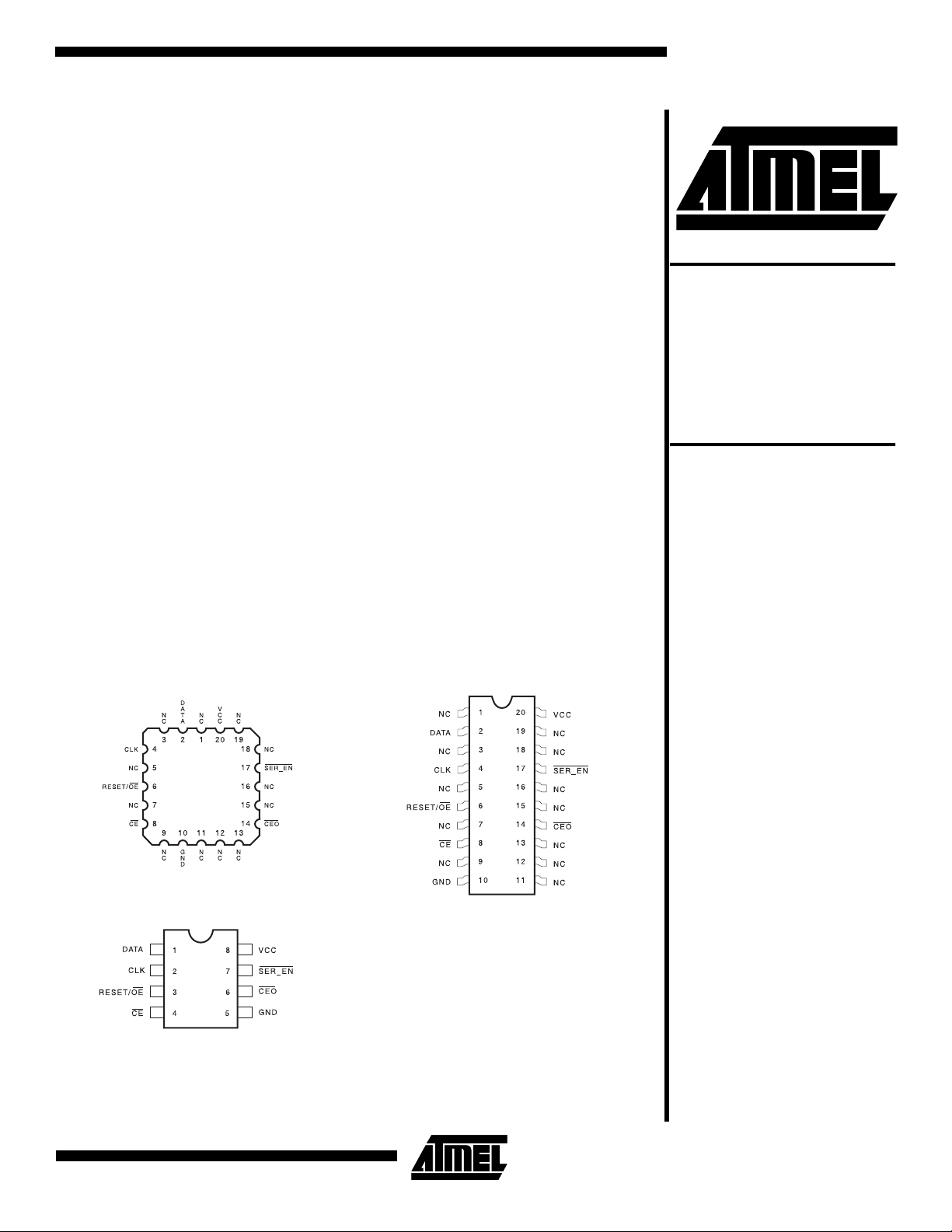
Pin Configurations
20-pin PLCC
20-Pin SOIC
65K, 128K and 256K
AT17C65
AT17C128
AT17C256
8-Pin DIP
0391E-A–5/97
1
Controlling The AT17 Series Serial EEPROMs
Most connections between the FPGA device and the Serial
EEPROM are simple and self-explanatory.
• The DATA output of the AT17 Series drives DIN of the
FPGA devices.
• The master FPGA CCLK output drives the CLK input of
the AT17 Series.
•The CEO
input of the next AT17C/LV128/256 in a cascade chain of
PROMs.
•SER_EN
There are, however, two different ways to use the inputs
and OE, as shown in the AC Characteristi cs wave-
CE
forms.
output of any AT17C/LV128/256 drives the CE
must be connected to VCC.
Condition 1
The simplest connection is to have the FPGA D/P output
drive both CE
its simplicity, however, this method will fail if the FPGA
receives an ext ernal reset condition during the co nfigura-
and RESET/OE in para ll el (F i gure 1 ). Due to
tion cycle. If a system r eset is a pplied t o the FPG A, it wi ll
abort the original configuration and then reset itself for a
new configuration, as intended. Of course, the AT17 Series
does not see the external reset signal and will not reset its
internal address counters and, consequently, will remain
out of sync with the FPGA for the remainder of the configuration cycle.
Condition 2
The FPGA D/P output drives only the CE input of the AT17
Series, while its O E
input to the FPGA RESET
under all normal circumstances, even when the user aborts
a configuration before D/P
the RESET/OE
reset – clears the Configurator's internal address pointer,
so that the reconfigurati on starts at the b eginning. The
AT17 Series does n ot requir e an inverte r sinc e the RE SET
polarity is programmable.
input is driven by the inversion of the
input pin. This connection wor ks
has gone High. A High level on
input to the AT17C/LVxxx – du ring FPGA
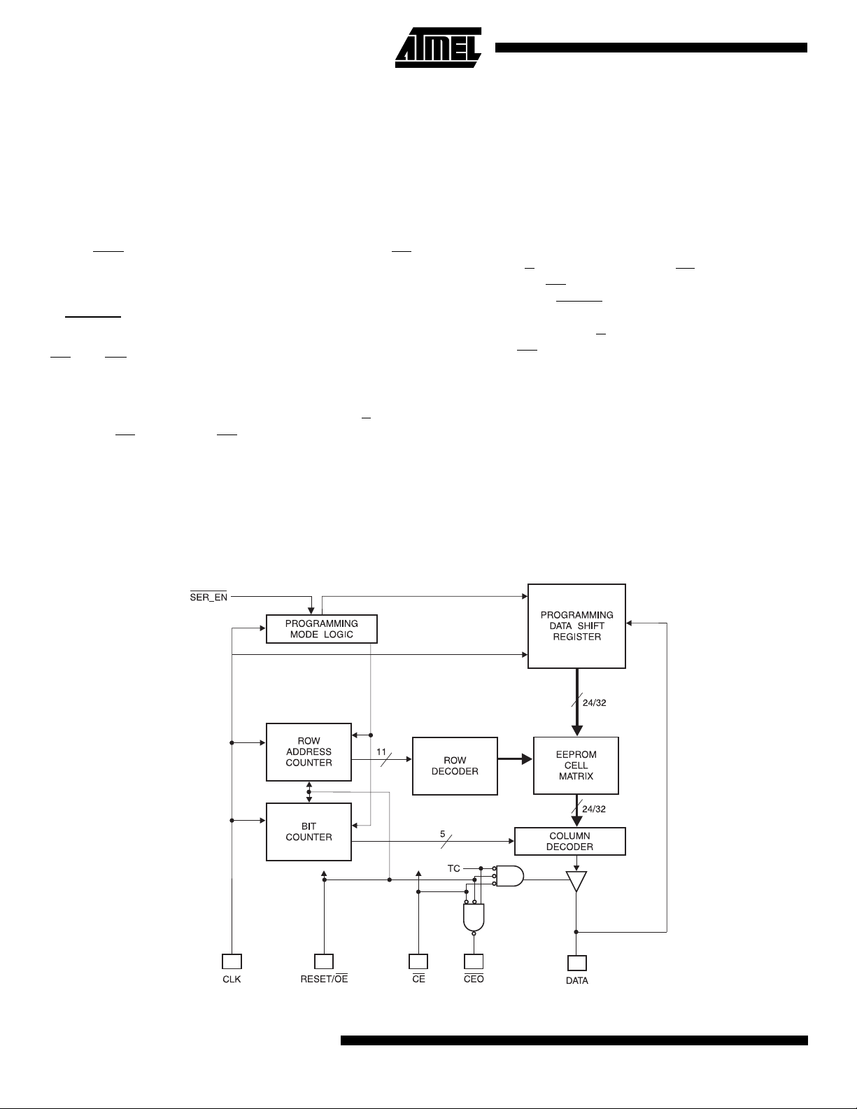
Block Diagram
2
AT17 Series
AT17 Series
Pin Configurations
PLCC/
SOIC DIP
Pin Pin Name I/O Description
2 1 DATA I/O Three-state DATA output for reading. Input/Output pin for programming.
42CLK I
Clock input. Used to increment the internal address and bit counter for reading
and programming.
RESET/Output Enable input (when SER_EN is High). A Low level on both the
CE
and RESET/OE inputs enables the data output driver. A High level on
63RESET/OE
RESET/OE
input is programmable as eith er RESET/OE
describes the pin as RESET/OE
84CE
I Chip Enable input. Used for device selection. A Low level on both CE and OE
enables the data output driver. A High level on CE
and bit counters and forces te device into a low power mode. Note this pin will
not enable/disable the device in 2-wire Serial mode (ie; when SER_EN
10 5 GND Ground Pin
14 6 CEO
O Chip Enable Out output. This signal is asserted Low on the clock cycle following
the last bit read from the memory. It will stay Low as long as CE and OE
both Low. It will then follow CE
High until the entire PROM is read again and senses the status of RESET
polarity.
A2 I Device selection input, A2. This is used to enable (or select) the device during
programming and when SER_EN
details).
17 7 SER_EN
Serial enable is normally high during FPGA loading operations. Bringing
I
SER_EN low, enables the 2-wire serial interface for programming.
resets both the addresss and bit counters. A logic polarity of this
or RESET/OE. This document
.
disables both the address
is Low).
are
until OE goes High. Thereafter CEO will stay
is Low (see Programming Guide for more
20 8 V
CC
+3.3V/+5V power supply pin.
Absolute Maximum Ratings*
Operating Temperature.........................-55°C to +125°C
Storage Temperature............................-65°C to +150°C
Voltage on Any Pin
with Respect to Ground.................... -0.1V to V
Supply Voltage (Vcc).............................. -0.5 V to +7.0V
Maximum Soldering Temp. (10 sec. @ 1/16 in.)...260°C
ESD (R
= 1.5K, C
ZAP
= 100pF) ........................2000V
ZAP
CC +
0.5V
*NOTICE: Stresses beyond those listed under “Absolute
Maximum Ratings” may cause permanent damage to the dev ice . This is a stress rating only an d
functional operati on of the de vi ce at these or an y
other conditions beyond those indicated in the
operational sections of this specification is not
implied. Exposure to absolute maximum rating
conditions f or exten ded periods ma y affect d evice
reliability .
3

FPGA Master Serial Mode Summary
The I/O and logic functions of the FPG A and their as sociated interconnections are established by a co nfiguration
program. The program is loaded either automatically upon
power up, or on comm and, depending on the state of th e
three FPGA mode pins. In Master Mode , the FPGA automatically loads th e conf igur ation progra m from an exter nal
memory. The Serial Configuration EEPROM has been
designed for compatibility with the Master Serial Mode.
Cascading Serial Configuration
EEPROMs
(AT17C/LV128 and AT17C/LV256)
For multiple FPGA s configured as a daisy-ch ain, or for
future FPGAs requiring larger configuration memories, cascaded Configurators provide additional memory (17C/
LV128 and 17C/LV256 only).
After the last bit fr om th e fi rst Con fig ur ator is read, the nex t
clock signal to the Configurator asserts its CEO
and disables its DATA line. The second Configurator recognizes the Low level on its CE
output.
Figure 1.
Condition 1 Connection
input and enables i ts DATA
output Low
After configuration is complete, the address counters of all
cascaded Configurators are reset if the reset signal drives
the RESET/OE
If the address counters are not to be reset upon completion, then the RE SET/O E
more details, please re ferenc e th e AT1 7C Se ri es Pr og ra mming Guide.
on each Configurator Active.
inputs can be tied to groun d. For
Programming Mode
The programming mode is entered b y bringing SE R_EN
Low. In this mode the chip can be programmed by the 2wire interface. The programming is done at V
only. Programming super voltages are generated inside the
chip. See the Programming Specification for Atmel's Configuration Memories Application Note for further information. The AT17C Series part s are read /write at 5V no minal .
The AT17LV parts are read/write at 3.0V nominal.
supply
CC
AT17C/LVXXX Reset Polarity
The AT17C/LVXXX lets the user choose the reset polarity
as either RESET/OE
or RESET/OE.
Standby Mode
The AT17C/LVXXX enters a low-power standby mode
whenever CE
tor consumes less than 1.0 mA of current. The output
remains in a high impedance state regardless of the state
of the OE
is asserted High. In this mode, the Configura-
input.
Operating Conditions
Symbol Description
Commercial
V
CC
4
Industrial
Military
AT17 Series
Supply voltage relative to GND
-0°C to +70°C
Supply voltage relative to GND
-40°C to +85C°
Supply voltage relative to GND
-55°C to +125C
AT17CXXX AT17LVXXX
UnitsMin/Max Min/Max
4.75/5.25 3.0/3.6 V
4.5/5.5 3.0/3.6 V
4.5/5.5 3.0/3.6 V

AT17 Series
µ
µ
µ
µ
µ
µ
DC Characteristics
VCC = 5V ± 5% Commercial / 5V ± 10% Ind./Mil.
Symbol Description Min Max Units
V
IH
V
IL
V
OH
V
OL
V
OH
V
OL
V
OH
V
OL
I
CCA
I
L
I
CCS
High-level input voltage 2.0 V
CC
Low-level input voltage 00.8V
High-level output voltage (IOH = -4 mA)
3.7 V
Commercial
Low-level output voltage (IOL = +4 mA) 0.32 V
High-level output voltage (IOH = -4 mA)
3.6 V
Industrial
Low-level output voltage (IOL = +4 mA) 0.37 V
High-level output voltage (IOH = -4 mA)
3.5 V
Military
Low-level output voltage (IOL = +4 mA) 0.4 V
Supply current, active mode 10 mA
Input or output leakage current (VIN = VCC or GND) -10 10
Commercial 75
Supply current, standby mode AT17C256
Industrial/Military 150
Commercial 1
Supply current, standby mode AT17C128/65
Industrial/Military 2
V
A
A
A
mA
mA
DC Characteristics
VCC = 3.3V ± 10%
Symbol Description Min Max Units
V
IH
V
IL
V
OH
V
OL
V
OH
V
OL
V
OH
V
OL
I
CCA
I
L
I
CCS
High-level input voltage 2.0 V
CC
Low-level input voltage 00.8V
High-level output voltage (IOH = -2.5 mA)
2.4 V
Commercial
Low-level output voltage (IOL = +3 mA) 0.4 V
High-level output voltage (IOH = -2 mA)
2.4 V
Industrial
Low-level output voltage (IOL = +3 mA) 0.4 V
High-level output voltage (IOH = -2 mA)
2.4 V
Military
Low-level output voltage (IOL = +2.5 mA) 0.4 V
Supply current, active mode 5mA
Input or output leakage current (VIN = VCC or GND) -10 10
Commercial 50
Supply current, standby mode
Industrial/Military 100
V
A
A
A
5

AC Characteristics
AC Characteristics When Cascading
6
AT17 Series

AC Characteristics for AT17C256
VCC = 5V ± 5% Commercial / VCC = 5V ± 10% Ind./Mil.
AT17 Series
Commercial Industrial/Military
Symbol Description
(2)
T
T
T
T
T
T
T
T
T
T
F
OE
CE
CAC
OH
DF
LC
HC
SCE
HCE
HOE
MAX
(2)
(2)
(3)
OE to Data Delay 25 25 ns
CE to Data Delay 45 45 ns
(2)
CLK to Data Delay 50 55 ns
Data Hold From CE, OE, or CLK 0 0 ns
CE or OE to Data Float Delay 50 50 ns
CLK Low Time 20 20 ns
CLK High Time 20 20 ns
CE Setup Time to CLK (to guarantee proper counting) 35 40 ns
CE Hold Time to CLk (to guarantee proper counting) 0 0 ns
OE High Time (guarantees counter is reset) 20 20 ns
MAX Input Clock Frequency 12.5 12.5 MHz
AC Characteristics for AT17C256 When Cascading
VCC = 5V± 5% Commercial / VCC = 5V ± 10% Ind./Mil.
UnitsMin Max Min Max
Symbol Description
(3)
T
CDF
T
OCK
T
OCE
T
OOE
Notes: 1. Preliminary specifications for military operating range only.
CLK to Data Float Delay 50 50 ns
(2)
CLK to CEO Delay 35 40 ns
(2)
CE to CEO Delay 35 35 ns
(2)
RESET/OE to CEO Delay 30 35 ns
2. AC test load = 50 pf.
3. Float delays are measu red with 5 pF AC loads. Transition is measured ±200 mV from steady state active levels.
Commercial Industrial/Military
UnitsMin Max Min Max
7

AC Characteristics for AT17C65/128
VCC = 5V ± 5% Commercial / VCC = 5V ± 10% Ind./Mil.
Commercial Industrial/Military
Symbol Description
(2)
T
T
T
T
T
T
T
T
T
T
F
OE
CE
CAC
OH
DF
LC
HC
SCE
HCE
HOE
MAX
(2)
(2)
(3)
OE to Data Delay 110 150 ns
CE to Data Delay 50 50 ns
(2)
CLK to Data Delay 50 55 ns
Data Hold From CE, OE, or CLK 0 0 ns
CE or OE to Data Float Delay 50 50 ns
CLK Low Time 30 35 ns
CLK High Time 30 35 ns
CE Setup Time to CLK (to guarantee proper counting) 45 50 ns
CE Hold Time to CLk (to guarantee proper counting) 0 5 ns
OE High Time (guarantees counter is reset) 50 60 ns
(4)
MAX Input Clock Frequency 10 10 MHz
AC Characteristics for AT17C65/128 When Cascading
VCC = 5V± 5% Commercial / VCC = 5V ± 10% Ind./Mil.
UnitsMin Max Min Max
Symbol Description
(3)
T
CDF
T
OCK
T
OCE
(2)
T
OE
Notes: 1. Preliminary specifications for military operating range only.
CLK to Data Float Delay 50 50 ns
(2)
CLK to CEO Delay 65 75 ns
(2)
CE to CEO Delay 55 60 ns
RESET/OE to CEO Dela y 55 55 ns
2. AC test load = 50 pf.
3. Float delays are measu red with 5 pF AC loads. Transition is measured ±200 mV from steady state active levels.
4. During cascade F
= 8 MHz.
MAX
Commercial Industrial/Military
Min Max Min Max
Units
8
AT17 Series

AC Characteristics
VCC = 3.3V ± 10%
AT17 Series
Commercial Industrial/Military
Symbol Description
(2)
T
OE
(2)
T
CE
T
CAC
(2)
T
OH
(3)
T
DF
T
LC
T
HC
T
SCE
T
HCE
T
HOE
F
MAX
Notes: 1. Preliminary specifications for military operating range only.
OE to Data Delay 40 45 ns
CE to Data Delay 60 60 ns
(2)
CLK to Data Delay 75 80 ns
Data Hold From CE, OE, or CLK 0 0 ns
CE or OE to Data Float Delay 55 55 ns
CLK Low Time 25 25 ns
CLK High Time 25 25 ns
CE Setup Time to CLK (to guarantee proper counting) 35 60 ns
CE Hold Time to CLk (to guarantee proper counting) 0 0 ns
OE High Time (guarantees counter is reset) 25 25 ns
(4)
MAX Input Clock Frequency 10 8 10 MHz
2. AC test lead = 50 pf.
3. Float delays are measured with 5 pF AC loads. Transition is measured ±200 mV afrom steady state active levels.
4. During cascade F
= 8 MHz.
MAX
UnitsMin Max Min Max
AC Characteristics When Cascading
VCC = 3.3V ± 10%
Symbol Description
(3)
T
T
T
T
CDF
OCK
OCE
OOE
CLK to Data Float Delay 60 60 ns
(2)
CLK to CEO Delay 55 60 ns
(2)
CE to CEO Delay 55 60 ns
(2)
RESET/OE to CEO Delay 40 45 ns
Commercial Industrial/M ilitary
Min Max Min Max
Units
9

Ordering Information - 5V Devices
Memory
Size (K) Ordering Code Package Operation Range
64K AT17C65-10PC
AT17C65-10JC
AT17C65-10SC
AT17C65-10PI
AT17C65-10JI
AT17C65-10SI
128K AT17C128-10PC
AT17C128-10JC
AT17C128-10SC
AT17C128-10PI
AT17C128-10JI
AT17C128-10SI
256K AT17C256-10PC
AT17C256-10JC
AT17C256-10SC
AT17C256-10PI
AT17C256-10JI
AT17C256-10SI
8P3
20J
20S
8P3
20J
20S
8P3
20J
20S
8P3
20J
20S
8P3
20J
20S
8P3
20J
20S
Commercial
(0°C to 70°C)
Industrial
(-40°C to 85°C)
Commercial
(0°C to 70°C)
Industrial
(-40°C to 85°C)
Commercial
(0°C to 70°C)
Industrial
(-40°C to 85°C)
Ordering Information - 3.3V Devices
Memory
Size (K) Ordering Code Package Operation Range
64K AT17LV65-10PC
AT17LV65-10JC
AT17LV65-10SC
AT17LV65-10PI
AT17LV65-10JI
AT17LV65-10SI
128K AT17LV128-10PC
AT17LV128-10JC
AT17LV128-10SC
AT17LV128-10PI
AT17LV128-10JI
AT17LV128-10SI
256K AT17LV256-10PC
AT17LV256-10JC
AT17LV256-10SC
AT17LV256-10PI
AT17LV256-10JI
AT17LV256-10SI
8P3 8-Lead, 0.300" Wide, Plastic Dual Inline Package (PDIP)
8P3
20J
20S
8P3
20J
20S
8P3
20J
20S
8P3
20J
20S
8P3
20J
20S
8P3
20J
20S
Package Type
Commercial
(0°C to 70°C)
Industrial
(-40°C to 85°C)
Commercial
(0°C to 70°C)
Industrial
(-40°C to 85°C)
Commercial
(0°C to 70°C)
Industrial
(-40°C to 85°C)
20J 20-Lead, Plastic J-Leaded Chip Carrier (PLCC)
20S 20-Lead, 0.300" Wide, Plastic Gull Wing Small Outline (SOIC)
10
AT17 Series
 Loading...