

AT16373
Fast Logic
16-Bit
Transparent
Latch
AT16373F
AT16373G
Features
••
Fastest Propagation Speeds in the Industry T
PD (F grade)
= 2.5 ns, T
PD (G grade)
= 2.0 ns
••
Maximum derating for capacitive loads 1.5ns/100 pF (F grade) and 1.1ns/100 pF
(G grade)
••
Very low ground bounce < 0.6V @ VCC=5.00V, Ta=25°C
••
Excellent noise rejection
••
Typical output skew ≤0.25ns
••
Bus Hold circuitry to retain last active state during Tri-state
•
Available in SSOP and TSSOP packages
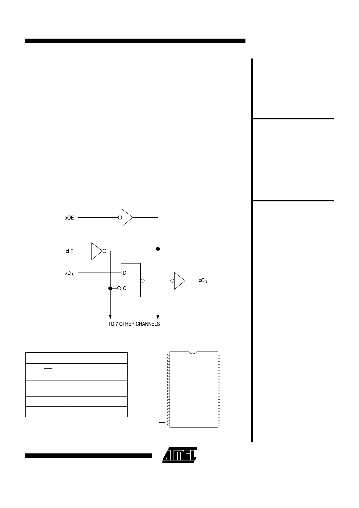
Description
Atmel’s AT16373 devices provide maximum speed in temporary data storage. They
can be operated as either two separat e 8 bit latches or as a single 16-bit latch by use
of the output enable and the lat ch enable. The AT16373 has very low ground bounce
and excellent i nput noise rejection, giving the user stable signals in a high speed
environment. These devices can drive very large loads while operating in a high speed
transparent mode.
Note: 1.This 8-bit latch function is repeated a second time on each device.
Functional Block Diagram
(1)
1
1O2
1O3
VCC
1O6
1O7
2O1
GND
2O4
2O5
GND
2O8
OE
1
3
5
7
9
11
13
15
17
19
21
23
47
45
43
41
39
37
35
33
31
29
27
25
48
46
44
42
40
38
36
34
32
30
28
26
2
4
6
8
10
12
14
16
18
20
22
24
1O1
GND
1O4
1O5
GND
1O8
2O2
2O3
VCC
2O6
2O7
2OE
1LE
1D2
1D3
VCC
1D6
1D7
2D1
GND
2D4
2D5
GND
2D8
1D1
GND
1D4
1D5
GND
1D8
2D2
2D3
VCC
2D6
2D7
2LE
Pin Names
Descriptions
xOE
Output Enable Input
(Active Low)
xLE
Latch Enable Inputs
(Active Hig h )
xD
χ
Data Inputs
xO
χ
Tri-State Outputs
Pin Configurations
SSOP/TSSOP
Top View
0756B
AT16373
5-15
Inputs Outputs
xDχ xLE xOE xOχ
HHLH
LHLL
XXHZ
Note: 1. X = Don’t Care, Z = High Impedance
Function Ta ble
(1)
Opera ting T empera ture. .. .... .. ............. ..0°C to +70 ° C
Storage Temperature......................-65°C to +150°C
Voltage on any Pin
with Respect to Ground ..................-2.0V to +7.0V
(1)
Maxi mu m Op e ra ting Vo l ta g e.............................6.0 V
*NOTICE: Stresses beyond those listed under “Absolute
Maximum Ratings” may cause permanent damage to
the device. This is a stress rating only and functional
operation of the device at these or any other conditions
beyond those indicated in the operational sections of
this specification is not implied. Exposure to absolute
maximum rating conditions for extended periods may
affect device reliability.
Notes:1.Minimum voltage is -0.6V dc which may undershoot
to -2.0V for pulses of less than 20 ns. Maximum
output pin voltage is V
CC
+0.75V dc which may
overshoot to +7.0V for pulses of less than 20 ns.
Absolute Maximu m Rating s*
Applicable over recommended operating range from Ta = 0°C to +70°C, VCC = +5.0V +/- 5% (unless otherwise noted)
Symbol
Parameter Test Conditions
Min Typ Max
Units
∆I
CC
Quiescent Power Supply
Current
VCC = Max, VIN = 3.4V 0.8 1.2 mA
V
IH
Input High Voltage 2.0 V
V
IL
Input Low Voltage 0.8 V
I
IH
Input High Current VIN = V
CC
±15 µA
I
IL
Inpu t Lo w Cu rrent VIN = GND ±15 µ A
I
OZ
Output Leakage Current ±10 µA
VOH(1) Output High Voltage
F Grade only
VCC = 4.75V
IOH = -10 mA
2.7 V
VOH(2)
Output High Voltage
G Grade only
VCC = 4.75V
IOH = -12 mA
2.7 V
V
OL
Output Low Volta ge ( F G ra de) IOL = 10 mA 0.55 V
V
OL
Output Low Volta ge ( G Grade) IOL = 12 mA 0.55 V
Note: 1. F grade: At V
CC (max)
, the value of V
OH(max)
= 3.75V and at V
CC(min)
, V
OH(max)
= 3.25V
2.G grade: At V
CC (max)
, the value of V
OH(max)
= 3.75V and at V
CC(min)
, V
OH(ma x )
= 3.35V
5.0 Volt DC Characteristics
5-16
AT16373

Applicable over recommended operating range from Ta = 0°C to +70°C, VCC = 5.0V +/- 5% (unless otherwise noted)
Symbol Parame ter Test Condi t ions
(1)
Min Typ Max Units
t
PHL
t
PLH
Propagation Delay xDχ to x Oχ CL = 50 pF 2.5 ns
t
PHL
t
PLH
Propagation Delay xLE to xOχ CL = 50 pF 5.5 ns
t
PZH
t
PZL
Output Enable CL = 50 pF 8.8 ns
t
PHZ
t
PLZ
Output Disa b le CL = 50 pF 6.5 ns
tSK(2) Output Skew CL = 50 pF 0.5 ns
∆t
PHL
(2)
∆t
PLH
Propagation Dela y vs Output Loading 1.3 1.5 ns/100 pF
t
su
Set-up Time CL = 50 pF 2.0 ns
t
H
Hold Time CL = 50 pF 2.0 ns
Note: 1.See test circuit and waveforms.
2.This parameter is guaranteed but not 100% tested.
AC Characteristics
AT16373F
Applicable over recommended operating r ange from Ta = 0°C to +70°C, VCC = 5.0V +/- 5% (unless otherwise noted)
Symbol Parameter Test Conditions
(1)
Min Typ Max Units
t
PHL
t
PLH
Propagation Delay xDχ to xOχ CL = 50 pF 2.0 ns
t
PHL
t
PLH
Propagation Delay xLE to xOχ CL = 50 pF 5.0 ns
t
PZH
t
PZL
Output Enable CL = 50 pF 8.8 ns
t
PHZ
t
PLZ
Output Disable CL = 50 pF
6.0
ns
tSK(2) Output Skew CL = 50 pF 0.5 ns
∆t
PHL
(2)
∆t
PLH
Propagation Delay vs Output Loading 0.9 1.1 ns/100 pF
t
su
Set-up Time CL = 50 pF 2.0 ns
t
H
Hold Time CL = 50 pF 2.0 ns
Note: 1.See test circuit and waveforms.
2.This parameter is guaranteed but not 100% tested.
AT16373G
AT16373
5-17

-40
0
40
80
120
160
Time
-1.0
-0.5
0.0
0.5
1.0
1.5
2.0
Output, V
I,mA
OL
2.5
3.0
3.5
4.0
I
OL
Output, V
IOL Pull Down Current
Pulse
Generator
V
IN
V
OUT
D.U.T.
V
CC
R
T
C
L
50 pF
500Ω
7.0V
500Ω
Note: 1. Puls e Gen era tor: Rate ≤ 1.0 MHz, tF ≤ 2.5 ns,
t
R
≤ 2.5 ns.
2.AC tests are done with a single bit switching, and
timings need to be derated when multiple outputs
are switching in the same direction simultaneously.
This derating should not exceed 0.5 ns for 16 inputs
switching simultaneously.
Test Circuits
(1,2)
Test Switch
Open Drain
Disable Low
Enable Low
Closed
All Other Tests Open
Definitions:
C
L
= Load capacitance; Includes jig and probe capacitance.
R
T
= Termination resistance; Should be equal to Z
OUT
of the
Pulse Generator.
Switch Position
3.5
Time
VOLV
VOLP
-0.5
0.0
0.5
1.0
1.5
2.0
2.5
3.0
Volts
gnd - measured on
output with input
held constant
output
Ground Bounce for High to Low
Transitions
(1)
VOHP
VOHV
0
0.5
1
1.5
2
2.5
3
3.5
4
4.5
Time
Volts
vcc measured on
output with
input held
constant
output
Supply Bounce for Low to High
Transitions
(2)
5-18
AT16373

Parameter Value Units
V
OLP
0.4 V
V
OLV
-0.26 V
V
OHV
VCC - 0. 13 V
V
OHP
VCC + 0.6 V
Note: 1.When multiple outputs are switched at the same time, rapidly changing current on the ground and VCC paths
causes a voltage to develop across the parasitic inductance of the wire bond and package pins. This occurrence
is called simultaneous switching noise. Atmel’s AT16373 products have minimized this phenomenon as shown on
the graph. Output data is for 15 outputs switching simultaneously at a frequency of 1 MHz. The ground data is
measured on the one remaining output, which is set to logic low and will reflect any device ground movement.
2.As on the graph for Ground Bounce, a similar condition occurs for low to high transitions. Output data is for 15 outputs
switching simultaneously at a frequency of 1 MHz. V
CC
droop is measured on the one remaining output pin, which is
set to a logic high. This output will reflect any movement on the device V
CC
.
Typical Va lu es
Input
Transition
1.5 V 1.5 V
VOH
1.5 V
VOL
Output
Transition
t
PLH
t
PHL
Propagation Delay Waveforms
Control
Input
Enable
Disable
3.0 V
3.5 V
0V
1.5 V
0V
0.3 V
0.3 V
1.5 V
Switch Open
Switch Closed
1.5 V
Output
Switched
Low
Output
Switched
High
t
PZL
t
PZH
t
PLZ
t
PHZ
V
OL
V
OH
Note: 1.Enable and disable waveforms are the same for both xOE and xLE inputs.
Enable and Disable Waveforms
(1)
AT16373
5-19

Ordering Information
T
PD
Ordering Co de Package Operation Ran ge
2.5 ns
AT16373F - 25YC
AT16373F - 25XC
48Y
48X
Commercial
2.0 ns
AT16373G - 20YC
AT16373G - 20XC
48Y
48X
Commercial
Package Type
48X
48 Pin, Plastic Thin Shrink Small Outline Package (TSSOP)
48Y
48 Pin, Plastic Shrink Small Outline Package (SSOP)
5-20
AT16373
 Loading...