AT16245
Fast Logic
Bi-Directional
Transceiver
AT16245F
AT16245G
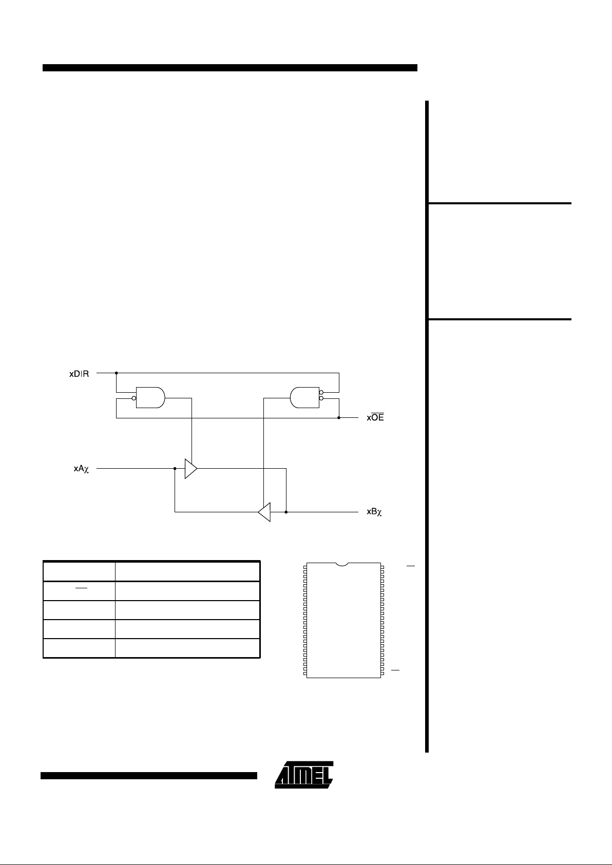
Functional Block Diagram
1DIR
1B2
1B3
VCC
1B6
1B7
2B1
GND
2B4
2B5
GND
2B8
1
3
5
7
9
11
13
15
17
19
21
23
47
45
43
41
39
37
35
33
31
29
27
25
48
46
44
42
40
38
36
34
32
30
28
26
2
4
6
8
10
12
14
16
18
20
22
24
1B1
GND
1B4
1B5
GND
1B8
2B2
2B3
VCC
2B6
2B7
2DIR
1
1A2
1A3
VCC
1A6
1A7
2A1
GND
2A4
2A5
GND
2A8
OE
1A1
GND
1A4
1A5
GND
1A8
2A2
2A3
VCC
2A6
2A7
2OE
Features
•
Fastest Propagation Speeds in the Industry T
PD (F grade)
= 2.5 ns,
T
PD (G grade)
= 2.0 ns
•
Maximum Derating for Capacitive Loads 1.5ns/100pF (F grade) and
1.1ns/100pF (G grade)
•
Very Low Ground Bounce <0.6V @ VCC=5.00 V, Ta=25°C
•
Excellent Noise Rejection
•
Typical Output Skew ≤0.25ns
•
Bus Hold Circuitry to Retain Last Active State During Tri-State
•
Available in SSOP and TSSOP Packages
Description
Atmel’s new family of high speed CMOS transceivers offers the best of all worlds to the
user requiring stability and ultra f ast sp eeds. T hese transceivers, which c an function as
two 8-bit devices or one 16-bit device, are capable of improving processing efficiency as
much as 6% by reducing the number of wait states required during memory access. In
addi tion, t his family of par ts has been desig ned to minim ize ground bounce on the out put s
while rejecting input spikes of up to 1.8V and 1 ns wide. This combination of ultra high
speed and low noise is th e next step i n high sp eed performance.
Pin Configurations
Pin Names Descriptions
xOE Output En able Input (Act ive Low)
xDIR Direction Control Input
xA
χ
Side A Inputs or Tri-State Outputs
xB
χ
Side B Inputs or Tri-State Outputs
SSOP/TSSOP
Top View
0754B
AT16245
5-9

Operating Temperature........................0°C to +7 0°C
Storage Temperatur e.............. . .......-65°C to +150°C
Voltage on any Pin
with Re s p e c t to Ground.. .. ............. -2.0 V to + 7 .0 V
(1)
Maxi mu m Op e ra ting Vo l tage..... .........................6.0V
Absolute Maximum Ratings*
NOTICE:Stresses beyond those listed under “Absolute
Maximum Ratings” may cause permanent damage to the
device. This is a stress rating only and functional operation
of the device at these or any other conditions beyond those
indicated in the operational sections of this specification is not
implied. Exposure to absolute maximum rating conditions for
extended periods may affect device reliability.
Notes: 1. Minimum voltage is -0.6V dc which may undershoot
to -2.0V for pulses of less than 20 ns. Maximum
output pin voltage is VCC +0.75V dc which may
overshoot to +7.0V for pulses of less than 20 ns.
5.0 Volt DC C haracteristics
Applicable over recommended operating range from Ta=0°C to +70° C, VCC=+5.0V ±5% (unless otherwise noted)
Symbol Parameter Test Conditio ns Min Typ Max Units
∆I
CC
Quiescent Power Supply Current VCC=Max, VIN=3.4V 0.8 1.2 mA
V
IH
Input High Voltage 2.0 V
V
IL
Input Low Voltage 0.8 V
I
IH
Input High Current (I/O Pins) VIN=V
CC
±15 µA
I
IL
Input Low Current (I/O Pins) VIN= GND ±15 µA
I
OZ
Output Leakage Current ±10 µA
V
OH
(1)
Output High Voltage
F Grade only
VCC=4.75 V
IOH=-10 mA
2.7 V
V
OH
(2)
Output High Voltage
G Grade only
VCC=4.75 V
IOH=-12 mA
2.7
V
V
OL
Output Low Voltage (F Grade) IOL=10 mA 0.55 V
V
OL
Output Low Voltage (G Grade) I
OL
=12 mA 0.55 V
Note: 1. F grade: At V
CC(max), the value of VOH(max)
= 3.75V and at V
CC(min)
, V
OH(max )
= 3.25V
2. G grade: At V
CC(max), the value of VOH(max)
= 3.75V and at V
CC(min)
, V
OH(max )
= 3.35V
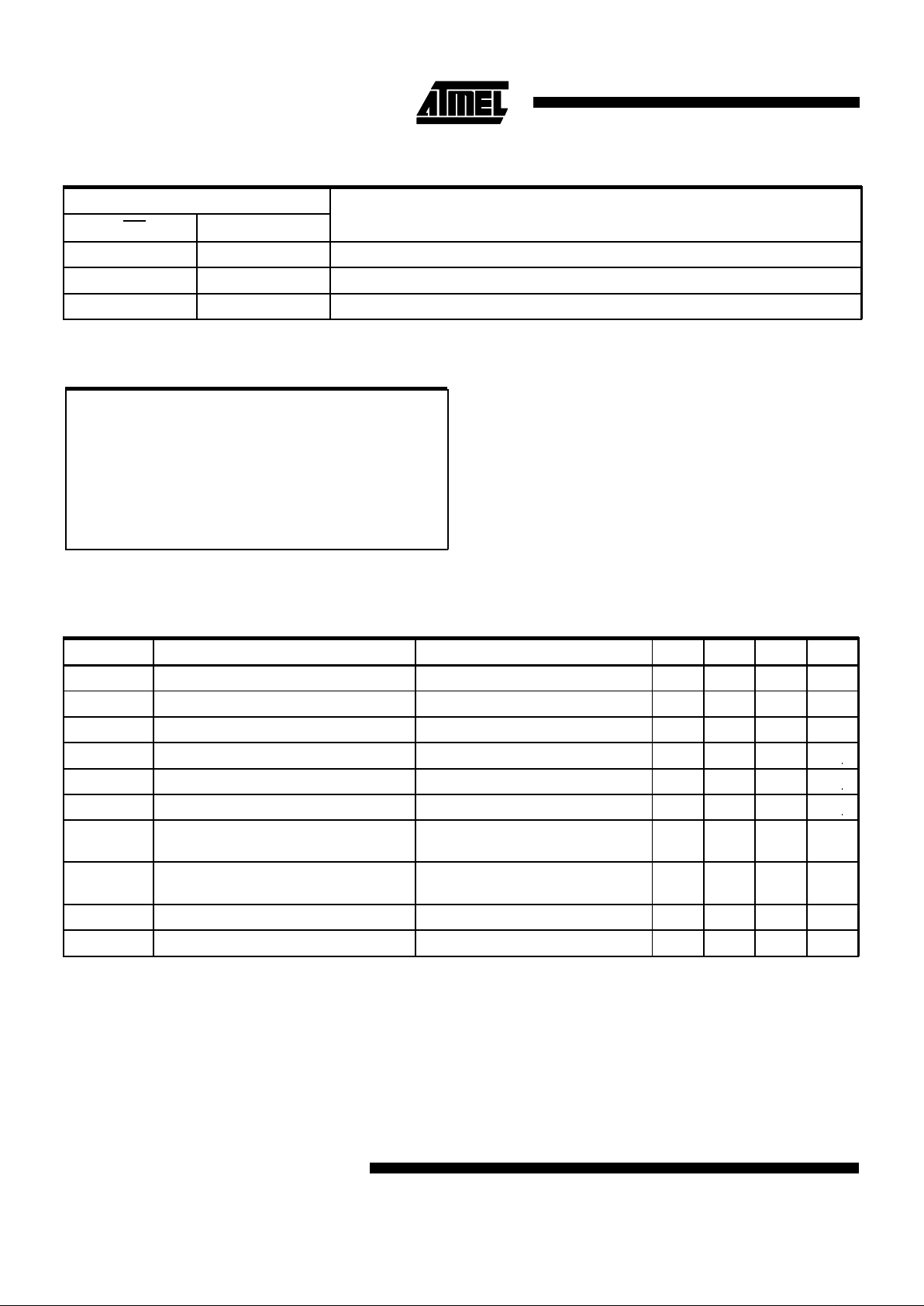
Function Table
Inputs
Outputs
xOE xDIR
L L Bus B Data to Bus A
L H Bus A Data to Bus B
HX
(1)
High Z State
Note: 1. X = Don’t Care
5-10
AT16245
 Loading...