

Page 1

ATAVRAUTO200
..............................................................................................
User Guide
Page 2

Table of Contents
Section 1
Introduction ........................................................................................... 1-1
1.1 Overview ...................................................................................................1-1
Section 2
Using the ATAVRAUTO200.................................................................. 2-3
2.1 Overview ...................................................................................................2-3
2.2 Power Supply ............................................................................................2-4
2.3 Oscillator Sources .....................................................................................2-4
2.4 On-board Resources.................................................................................2-4
2.5 In-System Programming ...........................................................................2-8
2.6 Debugging...............................................................................................2-11
Section 3
Technical Specifications ..................................................................... 3-13
Section 4
Technical Support............................................................................... 4-14
Section 5
Complete Schematics......................................................................... 5-17
ATAVRAUTO200 User Guide i
7698A–AUTO–01/07
Page 3
Section 1
Introduction
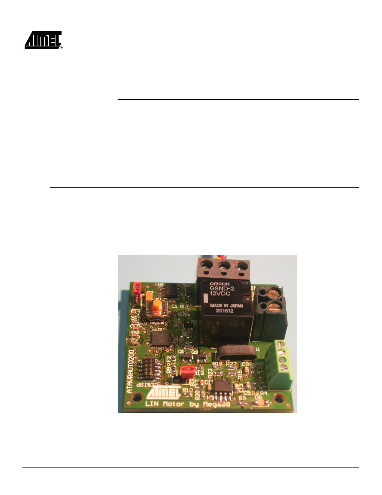
Congratulations on your purchase of the ATAVRAUTO200 board. This board includes
all elements necessary for designers to quickly develop code related to LIN communication node implementing the ATmega88 and for prototyping and testing of new designs.
1.1 Overview
This document describes the ATAVRAUTO200 dedicated to the ATmega88 AVR micro
controllers. This board is designed to allow an easy evaluation of the product using
demonstration firmware.
To increase its demonstrative capabilities, this stand alone board has numerous onboard resources (motor relay, motor FET, hall sensor inputs, current measurements,
power supply measurement, LIN, push buttons).
Figure 1-1. ATAVRAUTO200
ATAVRAUTO200 User Guide 1-1
7698A–AUTO–01/07
Page 4

Introduction
1.2 ATAVRAUTO200 features
The ATAVRAUTO200 provides the following features:
ATmega88 QFN32
AVR Studio® software interface
(1)
,
Power supply
– Regulated 5V
– From LIN connector (LIN network power supply)
JTAG connector:
– for on-chip In Situ Programming (ISP)
– for on-chip debugging using JTAG ICE
DC Motor connector
– DC Motor power supply output
– Hall effect sensor(s) power supply and input(s)
Serial interface:
– 1 LIN interface 1.3 and 2.0 compliant (firmware library available on the ATMEL
website for LIN 1.3).
On-board resources:
– 1 LIN transceiver with internal regulator
– Relay for DC motor control
– Shunt Resistor for motor current measurement
– Speed/Position measurement Inputs
– Power supply measurement
System clock:
– Internal RC oscillator
Dimension: 45 mm x 45 mm
Note: The ATmega88 is supported by AVR Studio, version 4.12 or higher. For up-to-
date information on this and other AVR tool products, please consult our web
site. The newest version of AVR Studio, AVR tools and this user guide can be
found in the AVR section of the Atmel web site, http://www.atmel.com.
1-2 ATAVRAUTO200 User Guide
7698A–AUTO–01/07
Page 5
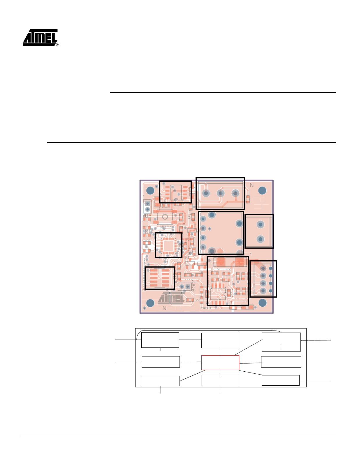
2.1 Overview
AT
AV
LIN
Connector
Motor Relay
Hall
Motor
Current
ATmega88
ISP
LIN
Measurement
Connector
Connector
Sensor
Transceiver
Regulator
Connector
ATmega88
JTAG
Power supply
Measurement
Lin Transceiver
Power supply
12 Vdc
from LIN
LIN
Network
DC Motor
Relay
Motor Shunt
Position sensor
Motor
Output
Motor ring
Hall sensor
ISP
ISP & Debugger
(AVR Studio)
ISP
(AVR Studio)
Section 2
Using the ATAVRAUTO200
Figure 2-1. Board Overview
Figure 2-2. Block Diagram
ATAVRAUTO200 User Guide 2-3
7698A–AUTO–01/07
Page 6

Using the ATAVRAUTO200
2.2 Power Supply
The on-board power supply circuitry is supplied through the LIN connector.
2.2.1 LIN powered The LIN connector power line is used to provide VBAT to the ATAVRAUTO200 LIN
transceiver.
A LIN network has to be connected to have your LIN interface function (Input supply
from 8 up to 18V DC, see Figure 2-3 on page 5) .
2.3 Oscillator Sources
The ATAVRAUTO200 board allows only one oscillator source:
Internal RC oscillator (Default configuration).
Note: The “Divide by 8” Fuse is configured by default. The first step in the demonstra-
tion application is to clear the prescaler to have the internal RC oscillator running at 8MHz:
CLKPR = (1<<CLKPCE); //! Clear Prescaler
CLKPR = 0;
2.3.1 Interal RC oscillatorn
A LIN Slave node with a run-time oscillator calibration can be used with the internal RC
oscillator.
At ambiant temperature and normal Vcc, the internal oscillator is precise enough to be
compliant with LIN 1.3 and 2.0 specifications. For wider temperature and/or power
ranges, a run-time calibration of the internal RC oscillator can be used as explained in
the application note AVR140: “ATMega48/88/168 family run-time calibration of the internal RC oscillator” available on the Atmel website.
2.4 On-board Resources
2.4.1 LIN & Power supply
The LIN screwed connector allows the user to select his own connector.
Note: The LIN power supply input is reverse voltage protected.
LIN transceiver control is realized by the micrcontroller. All modes depend on microcontroller’s ports configuration.
2-4 ATAVRAUTO200 User Guide
7698A–AUTO–01/07
Page 7
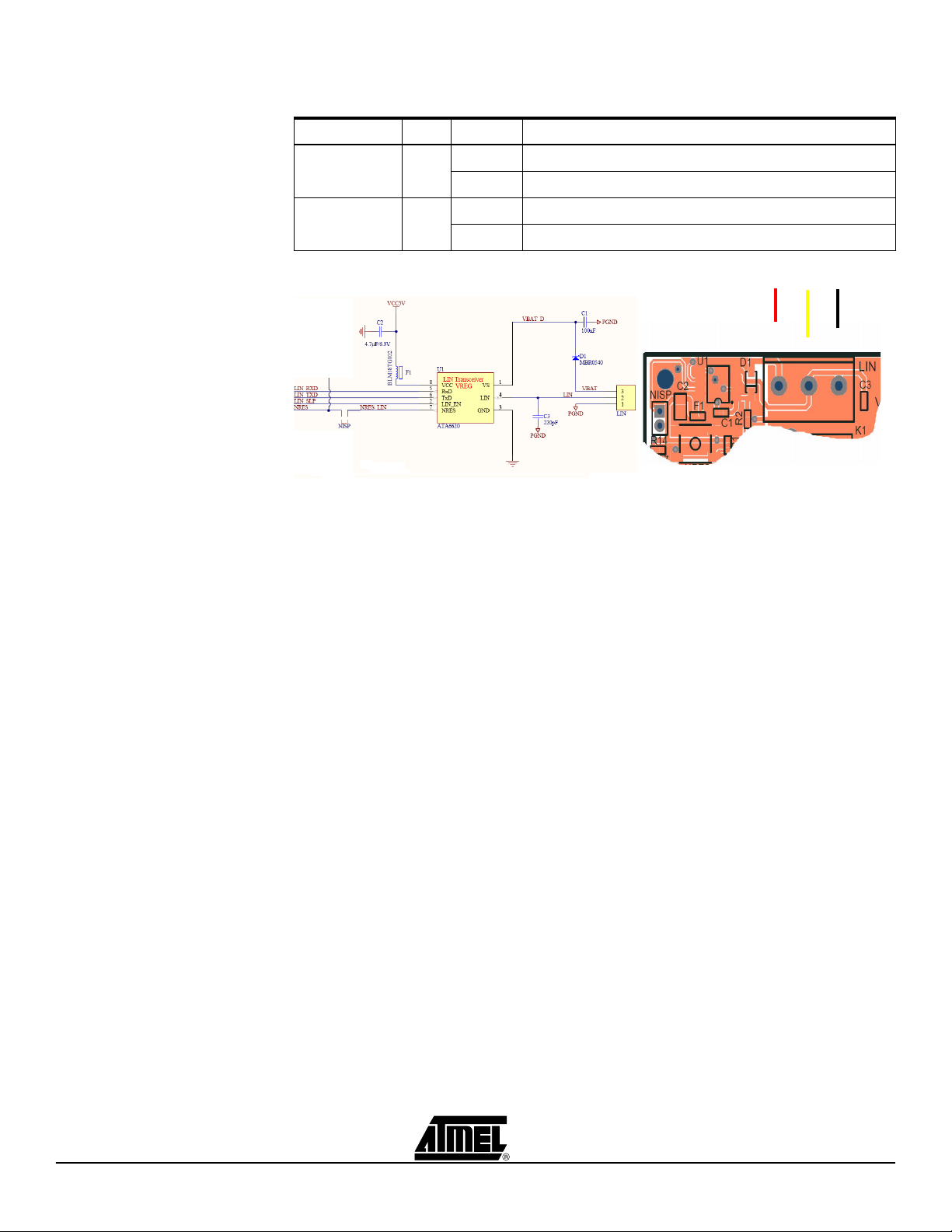
Using the ATAVRAUTO200
+VBat
G
N
D
L
I
N
V
IN
3.55 V
AD C
1
×=
Table 2-1. LIN ressources
Function Port State Description
LIN_NSLP PD2 Low LIN transceiver in Sleep mode
High LIN transceiver in normal mode
NRES_LIN PC6 Low Perform MCU reset when NISP Jumper is inserted
High No Action
Figure 2-3. LIN transceiver and power supply
Note: The LIN transceiver undervoltage protection can be disabled by removing the
NISP jumper.
Note: The NISP jumper has to be removed when programming.
2.4.2 Power supply measurement
The voltage measurement is realized with a bridge of resistors. The read value is 0.281
of the LIN power supply (47 KΩ / (47 KΩ + 120 KΩ)). Input voltage on channel 1 of the
ADC is limited to 5.1V by a zener diode. This will give a voltage reading range from 0 to
18.1V with Vcc as reference.
The power supply measurement can be performed using the A/D converter. See the
ATmega48/88/168 datasheet for how to use the ADC. The input voltage value (VIN) is
calculated with the following expression:
Where: V
V
ADC7
IN
= Input voltage value (V)
= Voltage value on ADC-1 input (V)
ATAVRAUTO200 User Guide 2-5
7698A–AUTO–01/07
Page 8

Using the ATAVRAUTO200
2.4.3 Motor relay
Figure 2-4. Power supply measurement through ADC1
DC Motor can be operated through a relay. It is supplied with Vbat, -Vbat or 0V.
The relay allows the motor to be operated in two rotating directions, or to be stopped.
Table 2-2. Motor Relay commands
Function Port State Description
Mot_A PB1 Low/ Relay coil1 OFF (Normaly closed switch activated)
High Relay coil1 ON (Normaly opened switch activated)
Mot_B PB2 Low Relay coil2 OFF (Normaly closed switch activated)
High Relay coil2 ON (Normaly opened switch activated)
Table 2-3. Logical command table
Mot_A Mot_B Motor Supply Description
L L 0V Motor stopped
L H -Vbat Motor running (Direction B)
H L +Vbat Motor running (DirectionA)
H H 0V Motor stopped
Figure 2-5. Motor on board command schematics
2-6 ATAVRAUTO200 User Guide
7698A–AUTO–01/07
Page 9

2.4.4 Current measurement
V
ADC-0
Ga i n V
shunt
Ga i n R shunt I××=× 30,16 0.005 I××= =( )
V
ADC-0
0.151 I×=
+Vcc
Hall1
Hall2
GND
Using the ATAVRAUTO200
Motor current is measured using a shunt resistor. External differential amplifier (on
board) is connected to ADC to measure shunt resistor voltage.
Amplifer output (current image voltage) is connected to
ADC0 pin for current acquisition
AIN1 pin to detect max current peak (compared to AIN0 through internal analog
comparator)
The current measurement (I) can be performed using the A/D converter. See the
ATmega48/88/168 datasheet for how to use the ADC. The input voltage value (V
ADC-0
is calculated with the following expression:
Analog comparator allows peak current detection. It provides interrupts on analog comparator output change. See the ATmega48/88/168 datasheet for how to use the Analog
comparator. Comparison voltage is determined for a 12A peak which leads to:
)
V
AIN0
= 1.5V
Figure 2-6. Current Acquisition chain and current Peak detection
2.4.5 Speed/Position measurement inputs
A screw connector with 4 inputs can be used to plug two hall effect sensors. The two hall
effect sensors inputs are connected to the two external interrupt pins (INT0 and INT1) of
the microcontroller.
Figure 2-7. Hall sensor effect interface
ATAVRAUTO200 User Guide 2-7
7698A–AUTO–01/07
Page 10

Using the ATAVRAUTO200
2.4.6 LED
2.4.7 BOOT
The ATAVRAUTO200 includes one green LED implemented on one I/O pin. It is connected to the “ PortD Pin3” of the ATm ega48/88/168. To light O n the LED, the
corresponding port pin must drive a low level. To light Off the LED, the corresponding
port pin must drive a high level.
Figure 2-8. LED schematic
An additional jumper (BOOT) has been added. This jumper is available for custom use.
For example : the BOOT jumper can be used to switch from the application to the bootloader by firmware (Not implemented in the example) by reading the pin7 of PortB.
Figure 2-9. BOOT Jumper
2.5 In-System Programming
The ATmega88 can be programmed using specific SPI serial links. This sub section
will explain how to connect the programmer.
The Flash, EEPROM memory (and all Fuse and Lock Bit options ISP-programmable)
can be programmed individually or with the sequential automatic programming option.
Note: If debugWire fuse is enabled, AVR ISP can’t be used. If debugWire fuse is dis-
Note: When programming, the NISP jumper has to be removed.
abled, JTAGICE mkII have to be used in ISP mode to enable debugWire fuse.
2-8 ATAVRAUTO200 User Guide
7698A–AUTO–01/07
Page 11

2.5.1 Using the ATAVRAUTO900 Adaptator
JTAGICE
ISP
The arrow has to be in front of the point
An additionnal adaptator has to be used to program the board using IPS or JTAG mode.
The 10 pins connector is used for the JTAGICE mkII device and the 6 pins connector is
used for the AVRISP device. To plug the ATAVRAUTO900 connector to the board, the
arrow (on the adaptator) has to be in front of the point (on the board).
Figure 2-10. ATAVRAUTO900 Connection
Table 2-4. ICE Connector
Using the ATAVRAUTO200
PIN Function
1 TCK
2 GND
3 TDO
4 VCC
5 TMS
6 NRES
7 VCC
8 NC
9 TDI
10 GND
Table 2-5. ISP Connector
PIN Function
1 MISO
2 VCC
3 SCK
4 MOSI
5 NRES
6 GND
ATAVRAUTO200 User Guide 2-9
7698A–AUTO–01/07
Page 12

Using the ATAVRAUTO200
AVR ISP
JTAGICE mkII
2.5.2 Programming with AVR ISP Programmer
The AVR ISP programmer is a compact and easy-to-use In-System Programming tool
for developing applications with ATmega88. Due to its small size, it is also an excellent
tool for field upgrades of existing applications. It is powered by the ATAVRAUTO200
and an additional power supply is thus not required.
The AVR ISP programming interface is integrated in AVR Studio.
To program the device using AVR ISP programmer, connect the AVR ISP to the adaptato r (A TA V RAUT O9 00 ) and co n ne ct th e ad a ptat or to the c on nec t or of the
ATAVRAUTO200.
Figure 2-11. Programming from AVR ISP programmer using ATAVRAUTO900.
Note: See AVR Studio® on-line Help for information.
2.5.3 Programming with AVR JTAGICEmkII
The ATmega48/88/168 can be programmed using specific JTAG link: 3-wire debugWIRE inte rfac e . To u se the AVR J T A GICEmkII w i t h an ATAVRAUTO200 thr
ATAVRAUTO900 adaptator has to be be used. Then the JTAG probe can be connected
to the ATAVRAUTO200 as shown in the following Figure 2-12.
To use the JTAGICEmkII in ISP mode the 3 jumpers “SCK”, “MISO” and “MOSI” of the
adaptator (ATAVRAUTO900) should be connected.
Figure 2-12. JTAGICE mkII probe connecting through debugWIRE interface
Note: When the debugWIRE Enable (DWEN) Fuse is programmed and Lock bits are
Note: See AVR Studio® on-line Help for information.
unprogrammed, the debugWIRE system within the target device is activated.
R E SE T p in i s c on f i g ur ed as co mm un ic a ti on ga t ew ay be tw e en
ATmega48/88/168 and JTAG. JTAGICE mkII must have control over it.
2-10 ATAVRAUTO200 User Guide
7698A–AUTO–01/07
Page 13

2.6 Debugging
2.6.1 Debugging with AVR JTAGICEmkII
The ATAVRAUTO200 can be used for debugging with JTAG ICE MK II.
Connect the JTAG ICE mkII as shown in Figure 2-12 for debugging, please refer to AVR
Studio Help information.
Using the ATAVRAUTO200
ATAVRAUTO200 User Guide 2-11
7698A–AUTO–01/07
Page 14

-12 ATAVRAUTO200 User Guide
7698A–AUTO–01/07
Page 15

Section 3
Technical Specifications
System Unit
– Physical Dimensions...............................................L=45 x W=45 x H=8 mm
– Weight ........................................................................................................25 g
Operating Conditions
– Internal Voltage Supply ..... ...................................................................... 5.0V
– External Voltage Supply .....................................................................7V -18V
ATAVRAUTO200 User Guide 3-13
7698A–AUTO–01/07
Page 16

Section 4
Technical Support
For Technical support, please contact avr@atmel.com. When requesting technical support, please include the following information:
Which target AVR device is used (complete part number)
Target voltage and speed
Clock source and fuse setting of the AVR
Programming method (ISP, JTAG or specific Boot-Loader)
Hardware revisions of the AVR tools, found on the PCB
Version number of AVR Studio. This can be found in the AVR Studio help menu.
PC operating system and version/build
PC processor type and speed
A detailed description of the problem
ATAVRAUTO200 User Guide 4-15
7698A–AUTO–01/07
Page 17

Section 5
Complete Schematics
On the next pages, the following documents of ATAVRAUTO200 are shown:
Complete schematics,
Bill of materials,
Assembly drawing.
ATAVRAUTO200 User Guide 5-15
7698A–AUTO–01/07
Page 18

Complete Schematics
Figure 5-1. ATAVRAUTO200 schematic
5-16 ATAVRAUTO200 User Guide
7698A–AUTO–01/07
Page 19

Figure 5-2. ATAVRAUTO200 Bill of Materials
Complete Schematics
ATAVRAUTO200 User Guide 5-17
7698A–AUTO–01/07
Page 20

Complete Schematics
LIN Motor by Mega88
C1
R10
C6
C4
R1
R12
Q1
BOOT
R16
R18
R5
R2
R20
U3
R3
C12
C11
R13
R23
R15C13
C5R6
DG
R4
R19 R22
Q2
D2
C8R8R7
HALL
R21
K1
C3
MOT
PM-06
V1.0
ATAVRAUTO200
C10
R17
NISP
R14
C7
C9
C2
ICE&ISP
U2
F1
NRES
R9 F2
U1
D1
LIN
Figure 5-3. ATAVRAUTO200 assembly drawing
5-18 ATAVRAUTO200 User Guide
7698A–AUTO–01/07
Page 21

© 2007 Atmel Corporation. All rights reserved.
Atmel®, logo and combinations thereof, Everywhere You Are
® ,
AVR®, AVR Studio® and others are
registered trademarks or trademarks of Atmel Corporation or its subsidiaries. Windows® and others are registered trademarks
or trademarks of Microsoft Corporation in the US and/or other countries. Other terms and product names may be trademarks of others.
Atmel Corporation Atmel Operations
2325 Orchard Parkway
San Jose, CA 95131, USA
Tel: 1(408) 441-0311
Fax: 1(408) 487-2600
Regional Headquarters
Europe
Atmel Sarl
Route des Arsenaux 41
Case Postale 80
CH-1705 Fribourg
Switzerland
Tel: (41) 26-426-5555
Fax: (41) 26-426-5500
Asia
Room 1219
Chinachem Golden Plaza
77 Mody Road Tsimshatsui
Eas t Kowloon
Hong Kong
Tel: (852) 2721-9778
Fax: (852) 2722-1369
Japan
9F, Tonetsu Shinkawa Bldg.
1-24-8 Shinkawa
Chuo-ku, Tokyo 104-0033
Japan
Tel: (81) 3-3523-3551
Fax: (81) 3-3523-7581
Memory
2325 Orchard Parkway
San Jose, CA 95131, USA
Tel: 1(408) 441-0311
Fax: 1(408) 436-4314
Microcontrollers
2325 Orchard Parkway
San Jose, CA 95131, USA
Tel: 1(408) 441-0311
Fax: 1(408) 436-4314
La Chantrerie
BP 70602
44306 Nantes Cedex 3, France
Tel: (33) 2-40-18-18-18
Fax: (33) 2-40-18-19-60
ASIC/ASSP/Smart Cards
Zone Industrielle
13106 Rousset Cedex, France
Tel: (33) 4-42-53-60-00
Fax: (33) 4-42-53-60-01
1150 East Cheyenne Mtn. Blvd.
Colorado Springs, CO 80906, USA
Tel: 1(719) 576-3300
Fax: 1(719) 540-1759
Scottish Enterprise Technology Park
Maxwell Building
Eas t Kilbride G75 0QR, Scotland
Tel: (44) 1355-803-000
Fax: (44) 1355-242-743
RF/Automotive
Theresienstrasse 2
Pos tfach 3535
74025 Heilbronn, Germany
Tel: (49) 71-31-67-0
Fax: (49) 71-31-67-2340
1150 East Cheyenne Mtn. Blvd.
Colorado Springs, CO 80906, USA
Tel: 1(719) 576-3300
Fax: 1(719) 540-1759
Biometrics/Imaging/Hi-Rel MPU/
High Speed Converters/RF Datacom
Avenue de Rochepleine
BP 123
38521 Saint-Egreve Cedex, France
Tel: (33) 4-76-58-30-00
Fax: (33) 4-76-58-34-80
Literature Requests
www.atmel.com/literature
Disclaimer: Atmel Corporation makes no w arranty for the use of its products, other t han those expressly contained in the Company’s standard
warranty which is detailed in Atmel’s Terms and Conditions located on the Compa ny’s web site. The Com pany assum es no responsibility for any
errors whic h may appear in this docu ment, reserves the right to change devices or specifications detailed herein at any time without notice, and
does not make any comm itment to update the information contained herein. No licenses to patents or other intellectual property of Atmel are
granted by the Company in conne ction with the sale of Atmel products, expressly or by implication. Atmel’s products are not authorized for use
as critical components in life support devices or systems .
Printed on recycled paper.
7698A–AUTO–01/07
/xM
 Loading...