


ATMEL ATV2500BQL-30LM-883, ATV2500BQL-30LM, ATV2500BQL-30KM-883, ATV2500BQL-30KM, ATV2500BQL-30DM-883 Datasheet
...
1
Note: For ATV2500BQ and
ATV2500BQL (PLCC/LCC
package only) pin 4 and
pin 26 connections are not
required.
Pin Configurations
Pin Name Function
IN Logic Inputs
CLK/IN Pin Clock and
Input
I/O Bidirectional
Buffers
I/O 0,2,4.. “Even” I/O Buffers
I/O 1,3,5.. “Odd” I/O Buffers
GND Ground
VCC +5V Supply
Features
•
High Performance, High Density Programmable Logic Device
– Typical 7 ns Pin-to-Pin Delay
– Fully Connected Logic Array With 416 Product Terms
•
Flexible Output Macrocell
– 48 Flip-Flops - Two per Macrocell
– 72 Sum Terms
– All Flip-Flops, I/O Pins Feed In Independently
– Achieves Over 80% Gate Utilization
•
Enhanced Macrocell Configuration Selections
– D- or T-Type Flip-Flops
– Product Te rm or Direct Input Pin Clocking
– Registered or Combinatorial Internal Feedback
•
Several Power Saving Options
•
Backward Compatible With ATV2500H/L Software
•
Proven and Reliable High Speed UV EPROM Process
•
Reprogrammable - Tested 100% for Programmability
•
40-Pin Dual-In-Line and 44-Pin Lead Surface Mount Packages
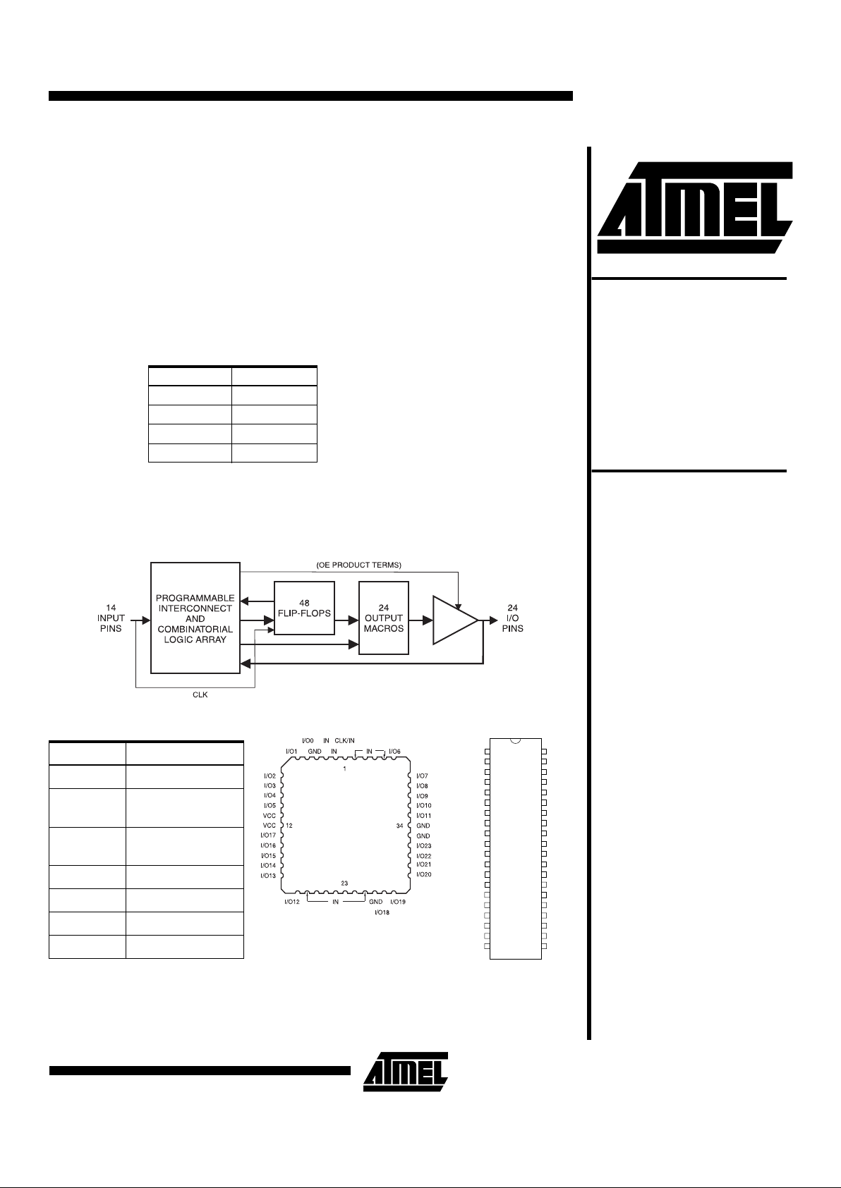
Block Diagram
Device ICC, Stand-By
ATV2500B 110 mA
ATV2500B Q 30 mA
ATV2500B L 2 mA
ATV2500B QL 2 mA
Rev. 0249F–06/98
High-Speed
High-Density
UV Erasable
Programmable
Logic Device
ATV2500B
DIP LCC/PLCC
1
2
3
4
5
6
7
8
9
10
11
12
13
14
15
16
17
18
19
20
40
39
38
37
36
35
34
33
32
31
30
29
28
27
26
25
24
23
22
21
CLK/IN
IN
IN
I/O0
I/O1
I/O2
I/O3
I/O4
I/O5
VCC
I/O17
I/O16
I/O15
I/O14
I/O13
I/O12
IN
IN
IN
IN
IN
IN
IN
IN
I/O6
I/O7
I/O8
I/O9
I/O10
I/O11
GND
I/O23
I/O22
I/O21
I/O20
I/O19
I/O18
IN
IN
IN
ATV2500B
2
Functional Logic Diagram ATV2500B
Note: 1. Not required for PLCC versions of ATV2500BQ or ATV2500BQL, making them compatible with ATV2500H and ATV2500L
pinout.

ATV2500B
3
Description
The ATV2500Bs are the highest density PLDs available in
a 40- or 44-pin package. With their fully connected l ogic
array and flexible macrocell structure, high gate utilization
is easily obtainable.
The ATV2500Bs are organized around a
single universal
and-or array
. All pin and feedback terms are always available to every macro ce ll. Eac h o f the 38 logic pins are array
inputs, as are the outputs of each flip-flop.
In the ATV2500Bs, four product terms are input to each
sum term. Furthermore, each macrocell's three sum terms
can be combined to provide up to 12 product terms per
sum term with
no performance penalty
. Each flip-flop is
individually se lecta ble to b e either D- or T -type, pr ovidin g
further logic compaction. Also, 24 of the flip-flops may be
bypassed to provide internal combinatorial feedback to the
logic array.
Product terms provide individual clocks and asynchronous
resets for each flip-flop. The flip-flops may also be individually configured to have direct input pin clocking. Each output has its own enable produc t term. Eight synchronous
preset product terms serve local groups of either four or
eight flip-flops. Register preload functions are provided to
simplify testing. All registers automatic ally reset upon
power up.
Several low power device options allow selection of the
optimum solution for many power -sensitive applic ations.
Each of the options significantly reduces total sy stem
power and enhances system reliability.
Functional Logic Diagram Description
The ATV2500B functional logic diagram describes the
interconnections betwee n the input, feedback p ins and
logic cells. All interc onnec tions are r outed th rough the si ngle global bus.
The ATV2500Bs are straightforward and uniform PLDs.
The 24 macrocells are numbered 0 through 23. Each macrocell contains 17 AND gates. All AND gates have 172
inputs. The five lower product terms provide AR1, CK1,
CK2, AR2, and OE. T hese are: one asy nchronous reset
and clock per flip-flop, and an output enable. The top 12
product terms are group ed i nto thr ee su m te rms, which are
used as shown in the macrocell diagram s.
Eight synchronous preset terms are distributed in a 2/4 pattern. The first four mac roc ell s s har e Pres et 0, t he nex t t w o
share Preset 1, a nd so on, end ing w ith th e last two ma crocells sharing Preset 7.
The 14 dedicated inputs an d their com plements use the
numbered positions in the global bus as shown. Each
macrocell provides six inputs to the global bus: (left to
right) feedback F2
(1)
true and false, flip-flop Q1 true and
false, and the pin true and false. The positions occupied by
these signals in the global bus are the six numb ers in the
bus diagram next to each macrocell.
Note: 1. Either the flip-flop input (D/T2) or output (Q2) may
be fed back in the ATV2500Bs.
ATV2500B
4
*NOTICE: Stresses beyond those listed under “Absolute Maxi-
mum Ratings” ma y cause permanent d amage to th e
device. This is a stress rating only and functional
operation of the device at these or any other conditions beyond those indicated in the operational sections of this specific ation is n ot implie d. Exposure to
absolute maximum rating conditions for extended
periods may affect device reliability.
Note: 1. Minimum voltage is -0.6V dc which may undershoot
to -2.0V for pulses o f less than 20ns . Maximum ou tput pin volt- age is V
CC
+0.75V dc which may over-
shoot to +7.0V for pulses of less than 20ns.
Absolute Maximum Ratings*
emperature Under Bias..................................-55°C to +125°C
Storage Temperature..................................... -65°C to +150°C
Voltage on Any Pin with
Respect to Ground ........................................-2.0V to +7.0V
(1)
Voltage on Input Pins
with Respect to Ground
During Programming....................................-2.0V to +14.0V
(1)
Programming Voltage with
Respect to Ground ......................................-2.0V to +14.0V
(1)
Integrated UV Erase Dose..............................7258 W•sec/cm
2
Note: 1. Typical values for nominal supply voltage. This parameter is only sampled and is not 100% tested.
DC and AC Operating Conditions
Commercial Industrial Military
Operating Temperature (Case) 0°C - 70°C -40°C - 85°C -55°C - 125°C
V
CC
Power Supply 5V ± 5% 5V ± 10% 5V ± 10%
Pin Capacitance
(f = 1 MHz, T = 25°C)
(1)
Typ Max Units Conditions
C
IN
46pFV
IN
= 0V
C
OUT
812pFV
OUT
= 0V
ATV2500B
5
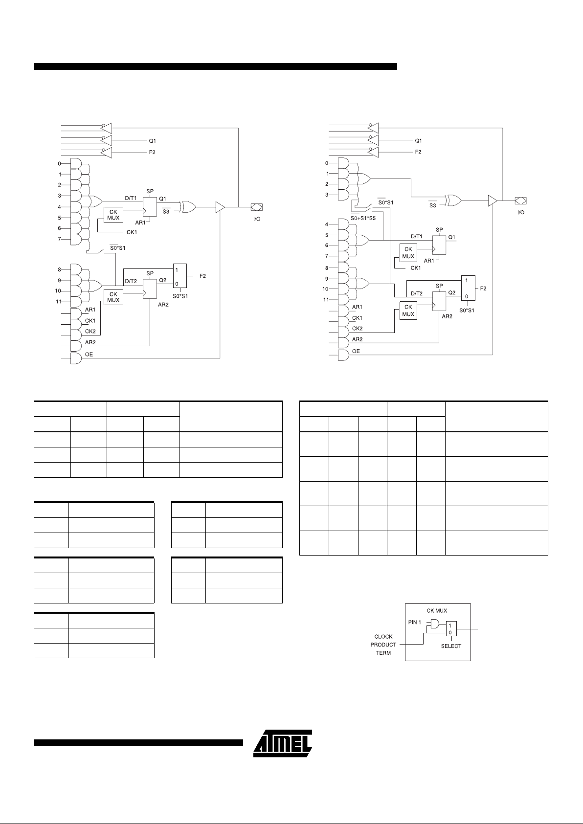
Output Logic, Registered
(1)
Output Logic, Combinatiorial
(1)
Note: 1. These diagrams show equivalent logic functions, not necessarily the actual circuit implementation.
Note: 1. These four terms are shared with D/T1.
Clock Option
S2 = 0 Terms in
Output ConfigurationS1 S0 D/T1 D/T2
0084Registered (Q1); Q2 FB
10124
(1)
Registered (Q1); Q2 FB
1184Registered (Q1); D/T2 FB
S3 Ouput Configuration S6 Q1 CLOCK
0 Ac tive Low 0 CK1
1 Active High 1 CK1 • PIN1
S4 Register 1 Type S7 Q2 CLOCK
0D 0CK2
1T 1CK2 • PIN1
S5 Register 2 Type
0D
1T
S2 = 1 Terms in
Output ConfigurationS5 S1 S0 D/T1 D/T2
X004
(1)
4
Combinatorial (8 Terms);
Q2 FB
X0144
Combinatorial (4 Terms);
Q2 FB
X104
(1)
4
(1)
Combinatorial (12 Terms);
Q2 FB
1114
(1)
4
Combinatorial (8 Terms);
D/T2 FB
01144
Combinatorial (4 Terms);
D/T2 FB
ATV2500B
6
Note: 1. See ICC versus frequency characterization curves.
DC Characteristics
Symbol Pa rameter Condition Min Typ Max Units
I
IL
Input Load Current VIN = -0.1V to VCC + 1V 10 µA
I
LO
Output Leakage
Current
V
OUT
= -0.1V to VCC + 0.1V 10 µA
I
CC
Power Supply
Current,
Standby
V
CC
= MAX,
V
IN
= GND or
V
CC
f = 0 MHz,
Outputs Open
ATV2500B
Com. 110 190 mA
Ind., Mil. 110 210 mA
ATV2500BQ
Com. 30 70 mA
Ind., Mil. 30 85 mA
ATV2500BL
Com. 2 5 mA
Ind., Mil. 2 10 mA
ATV2500BQL
Com. 2 4 mA
Ind., Mil. 2 5 mA
I
OS
Output Short
Circuit Current
V
OUT
= 0.5V -120 mA
V
IL
Input Low Voltage MIN ≤ VCC ≤ MAX -0.6 0.8 V
V
IH
Input High Voltage 2.0 VCC + 0.75 V
V
OL
Output Low Voltage
V
IN
= VIH or VIL,
V
CC
= 4.5V
IOL = 8 mA
Com.,
Ind.
0.5 V
I
OL
= 6 mA Mil. 0.5 V
V
OH
Output High
Voltage
V
CC
= MIN
I
OH
= -4.0 mA VCC - 0.3 V
I
OH
= -4.0 mA 2.4