

ATMEL ATV2500L-35PI, ATV2500L-35PC, ATV2500L-35LI, ATV2500L-35LC, ATV2500L-35KI Datasheet
...
1
Features
•
Third Generation Programmable Logic Structure
– Easily Achieves Gate Utilization Factors of 80 Percent
•
Increased Logic Flexibility
– 86 Inputs and 72 Sum Terms
•
Flexible Output Macrocell
– 48 Flip-Flops - 2 per Macrocell
– 3 Sum Terms - Can Be OR'ed and Shared
•
High-Speed
•
Low-Power — Less than 0.5 mA Typical (ATV2500L)
•
Multiple Feedback Paths Provide for Buried State Machines
and I/O Bus Compatibility
•
Asynchronous Clocks and Resets
– Multiple Synchronous Presets - One per Four or Eight Flip-Flops
•
Proven and Reliable High Speed CMOS EPROM Process
– 2000V ESD Protection
– 200 mA Latchup Immunity
•
Reprogrammable - Tested 100% for Programmability
•
40-pin Dual-In-line and 44-Lead Surface Mount Packages
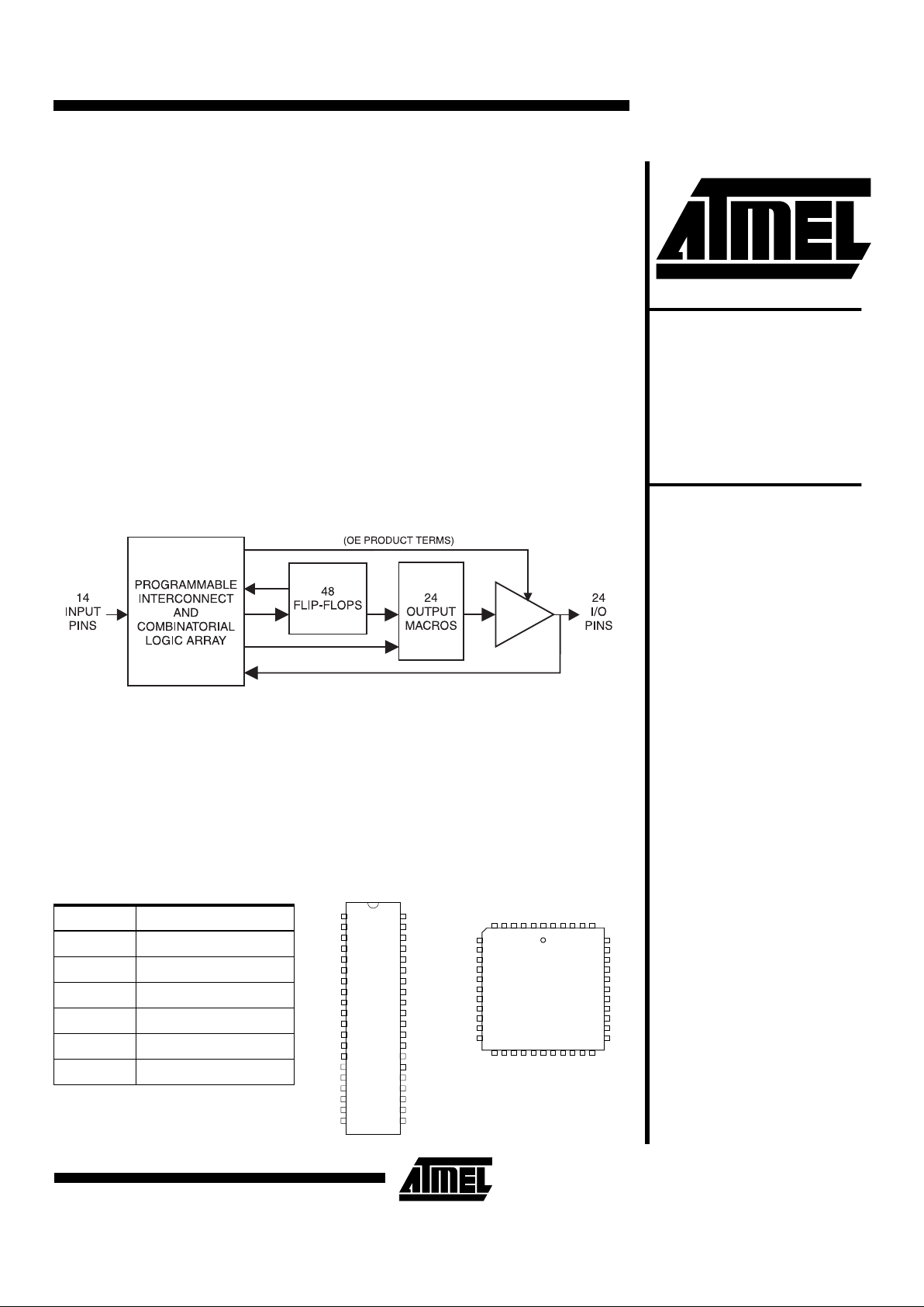
Block Diagram
Description
The ATV2500H/L is the most powerful programmable logic device available in a 40pin package. Increased product terms, sum terms, and flip-flops translate into many
more usable gates. High gate utilization is easily obtainable.
The ATV2500H/L is organized around a global bus. All pin and feedback terms are
always available to every logic cell. Each of the 38 logic pins and their complements
are array inputs, as well as the true and false outputs of each of the 48 flip-flops.
High-Density
UV-Erasable
Programmable
Logic Device
ATV2500H
ATV2500L
Rev. 0025E–05/98
(continued)
Pin Configurations
Pin Name Function
IN Logic Inputs
I/O Bidirectional Buffers
I/O, 0,2,4.. “Even” I/O Buffers
I/O, 1,3,5.. “Odd” I/O Buffers
* No Internal Connection
VCC +5V Supply
DIP
1
2
3
4
5
6
7
8
9
10
11
12
13
14
15
16
17
18
19
20
40
39
38
37
36
35
34
33
32
31
30
29
28
27
26
25
24
23
22
21
IN
IN
IN
I/O0
I/O1
I/O2
I/O3
I/O4
I/O5
VCC
I/O17
I/O16
I/O15
I/O14
I/O13
I/O12
IN
IN
IN
IN
IN
IN
IN
IN
I/O6
I/O7
I/O8
I/O9
I/O10
I/O11
GND
I/O23
I/O22
I/O21
I/O20
I/O19
I/O18
IN
IN
IN
PLCC/LCC
* = No Connect
7
8
9
10
11
12
13
14
15
16
17
39
38
37
36
35
34
33
32
31
30
29
I/O2
I/O3
I/O4
I/O5
VCC
VCC
I/O17
I/O16
I/O15
I/O14
I/O13
I/O7
I/O8
I/O9
I/O10
I/O11
GND
GND
I/O23
I/O22
I/O21
I/O20
65432
1
4443424140
1819202122232425262728
I/O12
INININININININ
*
I/O18
I/O19
I/O1
I/O0*INININININININ
I/O06
ATV2500H/L
2
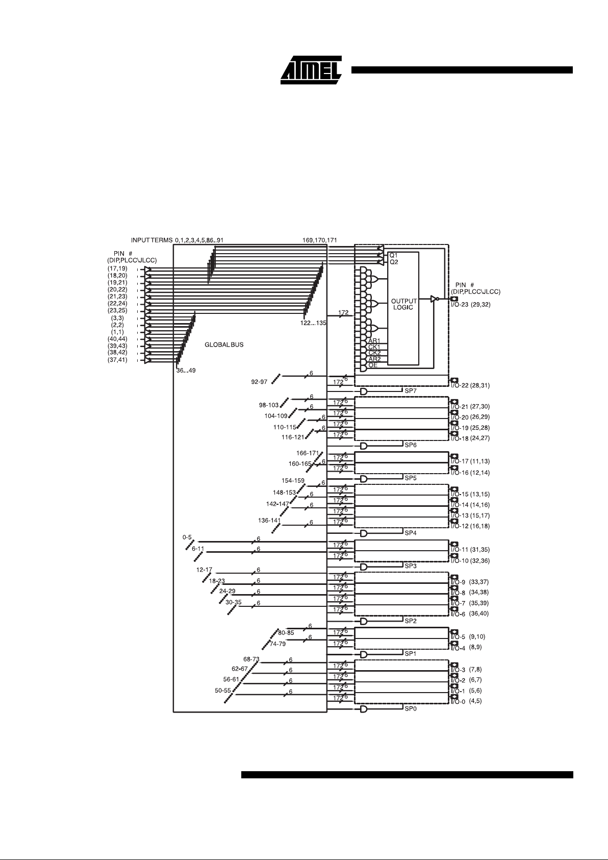
There are 416 product terms availab le. Four product terms
are input to each sum term. The three sum terms per logic
cell can be combined to provide up to twelve product terms,
combinatorial and registered. Independent of output configuration, the two flip-flops are always usable, and always
have at least four product term inputs.
Product terms are av ailable providing async hronous
resets, flip-flop clocks, and output enables. One reset and
one clock term are provi ded per flip-f lop, with one ena ble
term per output. Eight p ro duc t t erms pr ovide local synchronous presets, divided up in to bank s of f our and eight f lipflops. Registe r preload an d buried regis ter observ ability
simplify testi ng. The de vice has an inte rnal po wer up cle ar
function.
Functional Logic Diagram ATV2500H/L
ATV2500H/L
3
Functional Logic Diagram Description
The ATV2500H/L Functional Logic Diagram describes the
interconnections between the input, feedback p ins and
logic cells. All interconnections are routed through the global bus.
The ATV250 0H/L is a st raight forward and uniform PLD.
The twenty-four macr ocells are numbered 0 th rough 23.
Each macrocell conta ins 17 AND gates. A ll AND gates
have 172 inputs. The five lower product terms provide AR1,
CK1, CK2, AR2, and OE. These ar e: one asynchronous
reset and clock per fli p-flop, a nd an output ena ble. The top
twelve product te rms are group ed into th ree sum ter ms,
which are used as shown in the macrocell diagrams.
Eight synchronous preset terms are distributed in a 2/4 pattern. The first four macrocells share Preset 0, the next two
share Preset 1, a nd so on, end ing w ith th e last two ma crocells sharing Preset 7.
The fourteen dedicated inputs and their complements use
the numbered positions in the global bus as shown. Each
macrocell provides six inputs to the global bus: (left to right)
flip-flop Q2 true an d false, flip-flop Q1 true a nd false, and
the pin true and false. The positions occupied by these signals in the global bus are the six numbers in the bus diagram next to each macrocell.
Absolute Maximum Ratings*
Temperature Under Bias............................... -55°C to + 125°C
*NOTICE: Stresses beyond those listed under “Absolute
Maximum Ratings” may cause permanent damage to the dev ice. Th is is a s tress rating only an d
functional oper ati on of the device at t hes e o r any
other conditions beyond those indicated in the
operational sections of this specification is not
implied. Exposure to absolute maximum rating
conditions f or e xtended periods ma y af fect dev ice
reliability .
Note: 1. Minimum voltage is -0.6V dc, which may under-
shoot to -2.0V for pulses of less than 20 ns. Maximum output pin v oltage is Vcc + 0.75V dc , which
may overshoot to 7.0V for pulses of less than 20
ns.
Storage Temperature.................................... -65°C to + 150°C
Voltage on Any Pin with
Respect to Ground .........................................-2.0V to +7.0V
(1)
Voltage on Input Pins
with Respect to Ground
During Programming.....................................-2.0V to +14.0V
(1)
Programming Voltage with
Respect to Ground .......................................-2.0V to +14.0V
(1)
Integrated UV Erase Dose..............................7258 W.sec/cm
2
ATV2500H/L
4
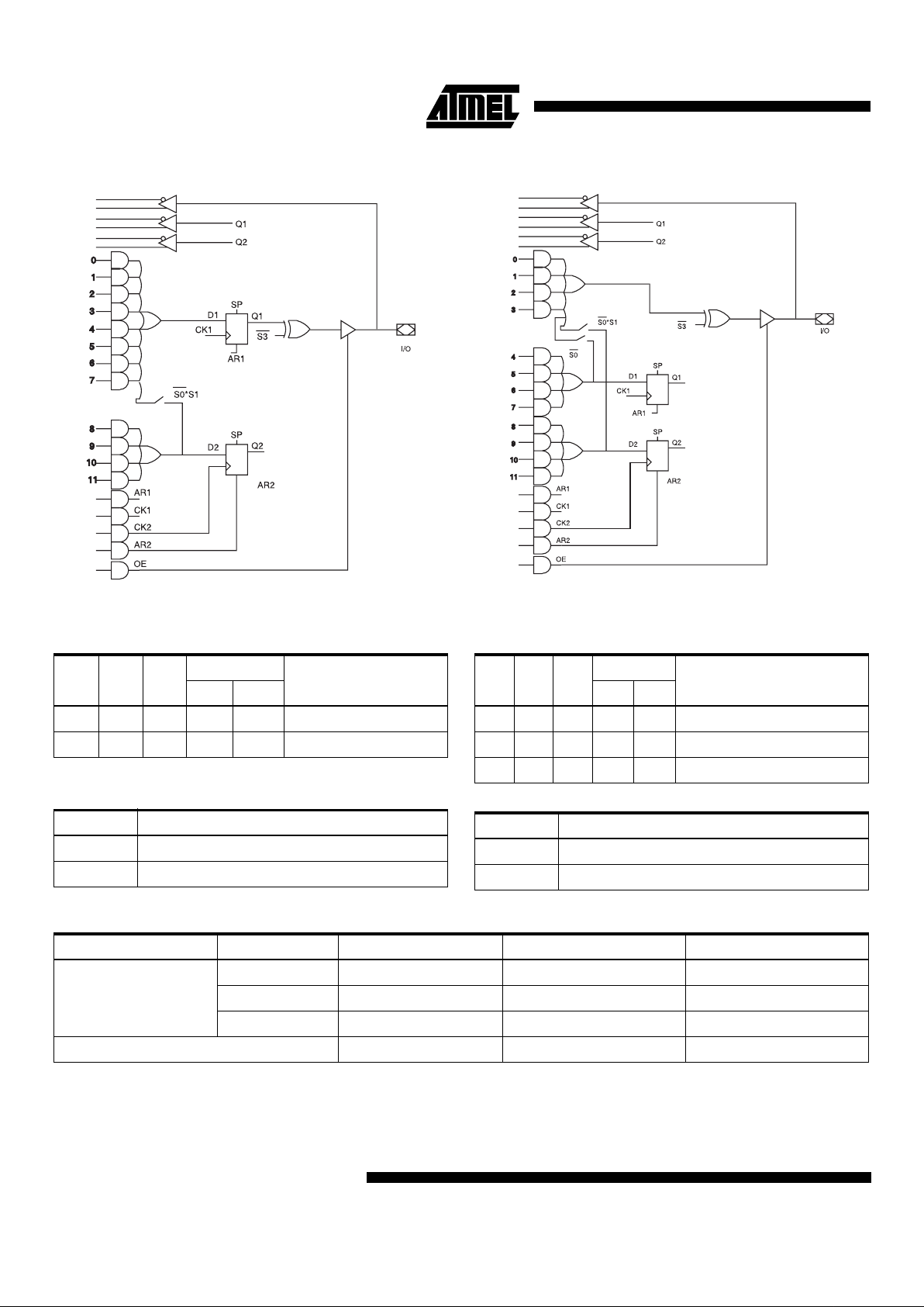
Output Logic, Registered Output Logic, Combinatorial
These diagrams show equivalent logic functions, not necessarily the actual circuit implementation.
Note: 1. These 4 terms are shared with D1.
Note: 1. These 4 terms are shared with D1.
S2 S1 S0
Te rms In
Output ConfigurationD1 D2
0 0 0 8 4 Registered (Q1)
010124
(1)
Registered (Q1)
S3 Output Configuration
0 Active Low
1 Active High
S2 S1 S0
Te rms In
Output ConfigurationD1 D2
1004
(1)
4 Combinatorial (8 Terms)
1 0 1 4 4 Combinatorial (4 Terms)
1104
(1)4(1)
Combinatorial (12 Terms)
S3 Output Configuration
0 Active Low
1 Active High
DC and AC Operating
ATV2500H-25 ATV2500H/L-30 ATV2500H/L-35
Operating
Temperature
(Case)
Com. 0°C - 70°C0
°
C - 70°C0
°
C - 70°C
Ind. -40°C - 85°C-40
°
C - 85°C-40
°
C - 85°C
Mil. -55°C - 125°C-55
°
C - 125°C-55
°
C - 125°C
VCC Power Supply 5V
±±±±
10% 5V
±±±±
10% 5V
±±±±
10%
ATV2500H/L
5
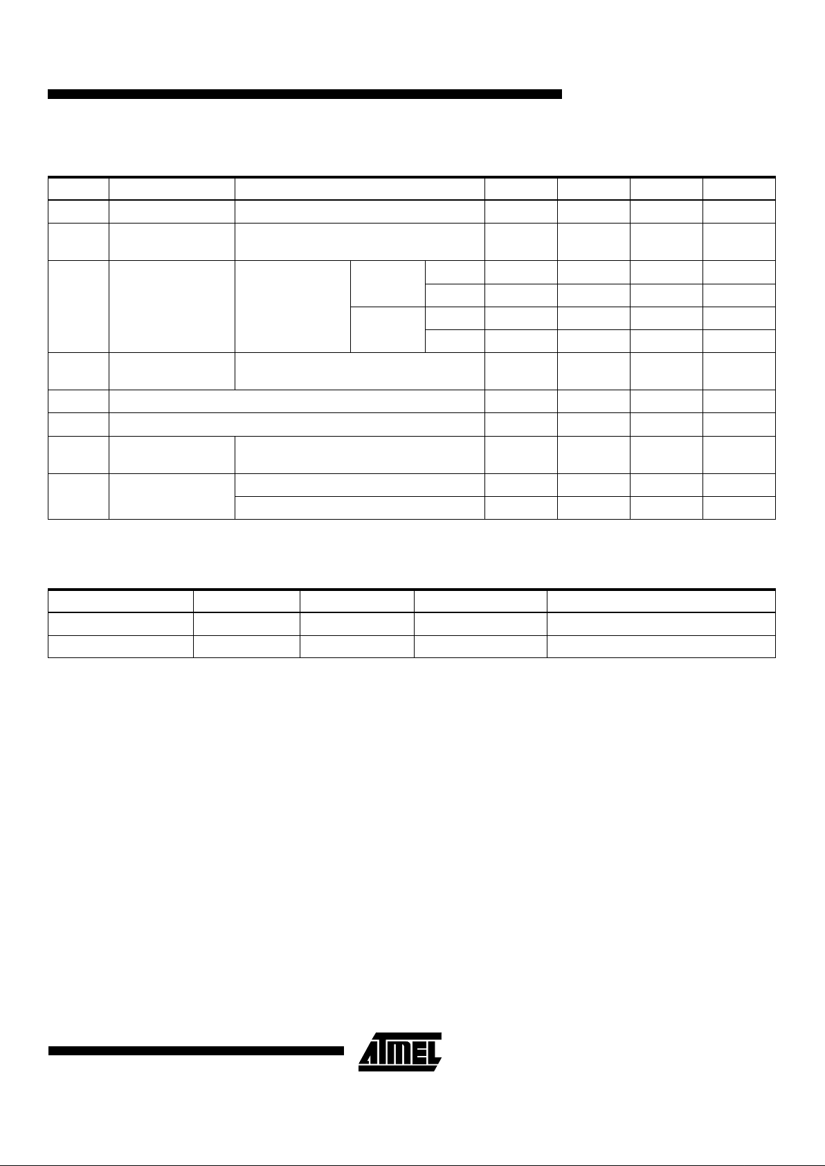
Note: 1. Not more than one output at a time should be shorted. Duration of short circuit test should not exceed 30 sec. This parame-
ter is only sampled and is not 100% tested. See Absolute Maximum Ratings.
Note: 1. Typical values for nominal supply voltage. This parameter is only sampled and is not 100% tested.
DC Characteristics
Symbol Parameter Condition Min Typ Max Units
I
LI
Input Load Current V
IN
= -0.1V to VCC + 1V 10 µA
I
LO
Output Leakage
Current
V
OUT
= -0.1V to VCC + 0.1V 10 µA
I
CC
Power Supply
Current
VCC = MAX,
V
IN
= GND or VCC
Outputs Open
ATV2500L Com. 0.5 5 mA
Ind.,Mil. 0.5 10 mA
ATV2500H Com. 80 160 mA
Ind.,Mil. 80 180 mA
I
OS
(1)
Output Short
Circuit Current
V
OUT
= 0.5V -120 mA
V
IL
Input Low Voltage -0.6 0.8 V
V
IH
Input High Voltage 2.0 V
CC
+ 0.75 V
V
OL
Output Low Voltage VIN = VIH or V
IL,
IOL = 8 mA Com,Ind; 6 mA Mil.
0.5 V
V
OH
Output High Voltage IOH = -100 µAV
CC
- 0.3 V
I
OH
= -4.0 mA 2.4 V
Pin Capacitance (f = MHz, T = 25
°°°°
C)
(1)
Ty p Max Units Conditions
C
IN
46 pF V
IN
= OV
C
OUT
812pF V
OUT
= OV
 Loading...