

Datasheet ATV2500L-35PI, ATV2500L-35PC, ATV2500L-35LI, ATV2500L-35LC, ATV2500L-35KI Datasheet (ATMEL)
...
1
Features
•
Third Generation Programmable Logic Structure
– Easily Achieves Gate Utilization Factors of 80 Percent
•
Increased Logic Flexibility
– 86 Inputs and 72 Sum Terms
•
Flexible Output Macrocell
– 48 Flip-Flops - 2 per Macrocell
– 3 Sum Terms - Can Be OR'ed and Shared
•
High-Speed
•
Low-Power — Less than 0.5 mA Typical (ATV2500L)
•
Multiple Feedback Paths Provide for Buried State Machines
and I/O Bus Compatibility
•
Asynchronous Clocks and Resets
– Multiple Synchronous Presets - One per Four or Eight Flip-Flops
•
Proven and Reliable High Speed CMOS EPROM Process
– 2000V ESD Protection
– 200 mA Latchup Immunity
•
Reprogrammable - Tested 100% for Programmability
•
40-pin Dual-In-line and 44-Lead Surface Mount Packages
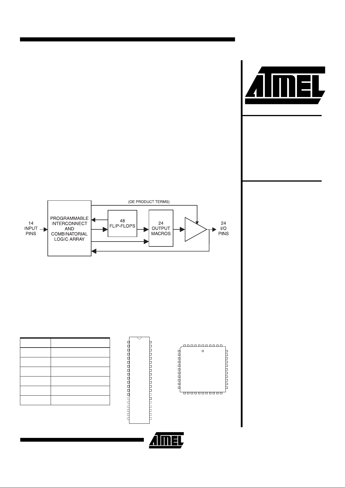
Block Diagram
Description
The ATV2500H/L is the most powerful programmable logic device available in a 40pin package. Increased product terms, sum terms, and flip-flops translate into many
more usable gates. High gate utilization is easily obtainable.
The ATV2500H/L is organized around a global bus. All pin and feedback terms are
always available to every logic cell. Each of the 38 logic pins and their complements
are array inputs, as well as the true and false outputs of each of the 48 flip-flops.
High-Density
UV-Erasable
Programmable
Logic Device
ATV2500H
ATV2500L
Rev. 0025E–05/98
(continued)
Pin Configurations
Pin Name Function
IN Logic Inputs
I/O Bidirectional Buffers
I/O, 0,2,4.. “Even” I/O Buffers
I/O, 1,3,5.. “Odd” I/O Buffers
* No Internal Connection
VCC +5V Supply
DIP
1
2
3
4
5
6
7
8
9
10
11
12
13
14
15
16
17
18
19
20
40
39
38
37
36
35
34
33
32
31
30
29
28
27
26
25
24
23
22
21
IN
IN
IN
I/O0
I/O1
I/O2
I/O3
I/O4
I/O5
VCC
I/O17
I/O16
I/O15
I/O14
I/O13
I/O12
IN
IN
IN
IN
IN
IN
IN
IN
I/O6
I/O7
I/O8
I/O9
I/O10
I/O11
GND
I/O23
I/O22
I/O21
I/O20
I/O19
I/O18
IN
IN
IN
PLCC/LCC
* = No Connect
7
8
9
10
11
12
13
14
15
16
17
39
38
37
36
35
34
33
32
31
30
29
I/O2
I/O3
I/O4
I/O5
VCC
VCC
I/O17
I/O16
I/O15
I/O14
I/O13
I/O7
I/O8
I/O9
I/O10
I/O11
GND
GND
I/O23
I/O22
I/O21
I/O20
65432
1
4443424140
1819202122232425262728
I/O12
INININININININ
*
I/O18
I/O19
I/O1
I/O0*INININININININ
I/O06
ATV2500H/L
2
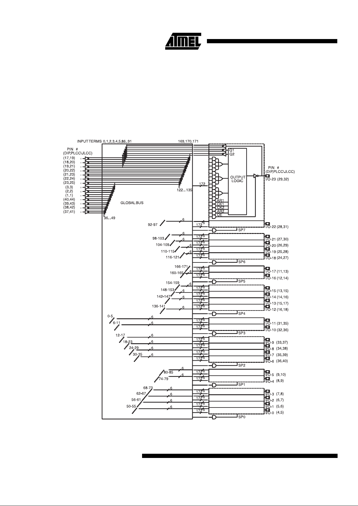
There are 416 product terms availab le. Four product terms
are input to each sum term. The three sum terms per logic
cell can be combined to provide up to twelve product terms,
combinatorial and registered. Independent of output configuration, the two flip-flops are always usable, and always
have at least four product term inputs.
Product terms are av ailable providing async hronous
resets, flip-flop clocks, and output enables. One reset and
one clock term are provi ded per flip-f lop, with one ena ble
term per output. Eight p ro duc t t erms pr ovide local synchronous presets, divided up in to bank s of f our and eight f lipflops. Registe r preload an d buried regis ter observ ability
simplify testi ng. The de vice has an inte rnal po wer up cle ar
function.
Functional Logic Diagram ATV2500H/L

ATV2500H/L
3
Functional Logic Diagram Description
The ATV2500H/L Functional Logic Diagram describes the
interconnections between the input, feedback p ins and
logic cells. All interconnections are routed through the global bus.
The ATV250 0H/L is a st raight forward and uniform PLD.
The twenty-four macr ocells are numbered 0 th rough 23.
Each macrocell conta ins 17 AND gates. A ll AND gates
have 172 inputs. The five lower product terms provide AR1,
CK1, CK2, AR2, and OE. These ar e: one asynchronous
reset and clock per fli p-flop, a nd an output ena ble. The top
twelve product te rms are group ed into th ree sum ter ms,
which are used as shown in the macrocell diagrams.
Eight synchronous preset terms are distributed in a 2/4 pattern. The first four macrocells share Preset 0, the next two
share Preset 1, a nd so on, end ing w ith th e last two ma crocells sharing Preset 7.
The fourteen dedicated inputs and their complements use
the numbered positions in the global bus as shown. Each
macrocell provides six inputs to the global bus: (left to right)
flip-flop Q2 true an d false, flip-flop Q1 true a nd false, and
the pin true and false. The positions occupied by these signals in the global bus are the six numbers in the bus diagram next to each macrocell.
Absolute Maximum Ratings*
Temperature Under Bias............................... -55°C to + 125°C
*NOTICE: Stresses beyond those listed under “Absolute
Maximum Ratings” may cause permanent damage to the dev ice. Th is is a s tress rating only an d
functional oper ati on of the device at t hes e o r any
other conditions beyond those indicated in the
operational sections of this specification is not
implied. Exposure to absolute maximum rating
conditions f or e xtended periods ma y af fect dev ice
reliability .
Note: 1. Minimum voltage is -0.6V dc, which may under-
shoot to -2.0V for pulses of less than 20 ns. Maximum output pin v oltage is Vcc + 0.75V dc , which
may overshoot to 7.0V for pulses of less than 20
ns.
Storage Temperature.................................... -65°C to + 150°C
Voltage on Any Pin with
Respect to Ground .........................................-2.0V to +7.0V
(1)
Voltage on Input Pins
with Respect to Ground
During Programming.....................................-2.0V to +14.0V
(1)
Programming Voltage with
Respect to Ground .......................................-2.0V to +14.0V
(1)
Integrated UV Erase Dose..............................7258 W.sec/cm
2
ATV2500H/L
4
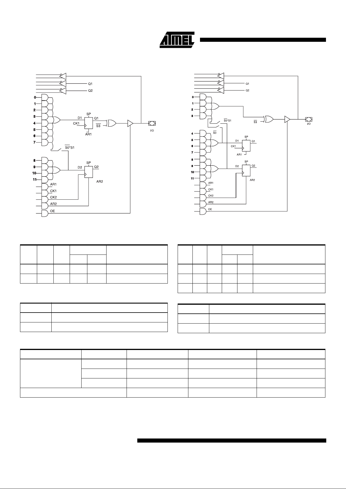
Output Logic, Registered Output Logic, Combinatorial
These diagrams show equivalent logic functions, not necessarily the actual circuit implementation.
Note: 1. These 4 terms are shared with D1.
Note: 1. These 4 terms are shared with D1.
S2 S1 S0
Te rms In
Output ConfigurationD1 D2
0 0 0 8 4 Registered (Q1)
010124
(1)
Registered (Q1)
S3 Output Configuration
0 Active Low
1 Active High
S2 S1 S0
Te rms In
Output ConfigurationD1 D2
1004
(1)
4 Combinatorial (8 Terms)
1 0 1 4 4 Combinatorial (4 Terms)
1104
(1)4(1)
Combinatorial (12 Terms)
S3 Output Configuration
0 Active Low
1 Active High
DC and AC Operating
ATV2500H-25 ATV2500H/L-30 ATV2500H/L-35
Operating
Temperature
(Case)
Com. 0°C - 70°C0
°
C - 70°C0
°
C - 70°C
Ind. -40°C - 85°C-40
°
C - 85°C-40
°
C - 85°C
Mil. -55°C - 125°C-55
°
C - 125°C-55
°
C - 125°C
VCC Power Supply 5V
±±±±
10% 5V
±±±±
10% 5V
±±±±
10%
ATV2500H/L
5
Note: 1. Not more than one output at a time should be shorted. Duration of short circuit test should not exceed 30 sec. This parame-
ter is only sampled and is not 100% tested. See Absolute Maximum Ratings.
Note: 1. Typical values for nominal supply voltage. This parameter is only sampled and is not 100% tested.
DC Characteristics
Symbol Parameter Condition Min Typ Max Units
I
LI
Input Load Current V
IN
= -0.1V to VCC + 1V 10 µA
I
LO
Output Leakage
Current
V
OUT
= -0.1V to VCC + 0.1V 10 µA
I
CC
Power Supply
Current
VCC = MAX,
V
IN
= GND or VCC
Outputs Open
ATV2500L Com. 0.5 5 mA
Ind.,Mil. 0.5 10 mA
ATV2500H Com. 80 160 mA
Ind.,Mil. 80 180 mA
I
OS
(1)
Output Short
Circuit Current
V
OUT
= 0.5V -120 mA
V
IL
Input Low Voltage -0.6 0.8 V
V
IH
Input High Voltage 2.0 V
CC
+ 0.75 V
V
OL
Output Low Voltage VIN = VIH or V
IL,
IOL = 8 mA Com,Ind; 6 mA Mil.
0.5 V
V
OH
Output High Voltage IOH = -100 µAV
CC
- 0.3 V
I
OH
= -4.0 mA 2.4 V
Pin Capacitance (f = MHz, T = 25
°°°°
C)
(1)
Ty p Max Units Conditions
C
IN
46 pF V
IN
= OV
C
OUT
812pF V
OUT
= OV

ATV2500H/L
6
AC Waveforms
(1)
Note: 1. Timing measurement reference is 1.5V. Input AC driving levels are 0.0V and 3.0V, unless otherwise specified.
Note: 1. Buried registers include all 24 Q2 registers and any of the 24 Q1 registers in macrocells configured as combinatorial.
AC Characteristics for the ATV2500L
Symbol Parameter
ATV2500L-30 ATV2500L-35
UnitsMin Max Min Max
t
PD
Input or Feedback to
Non-Registered Output
30 35 ns
t
EA
Input to Output Enable 30 35 ns
t
ER
Input to Output Disable 30 35 ns
t
CO
Clock to Output 5 30 5 35 ns
t
CF
Clock to Feedback 10 20 15 20 ns
t
SI1
Input Setup Time, Output Register 20 22 ns
t
SI2
Input Setup
Time, Buried Register
(1)
20 22 ns
t
SF
Feedback Setup Time 10 15 ns
t
H1
Hold Time, Output Register 10 15 ns
t
H2
Hold Time, Buried Register
(1)
55ns
t
W
Clock Width 15 17 ns
t
P
Clock Period 30 35 ns
F
MAX
Maximum Frequency (1/tP)3328MHz
t
AW
Asynchronous Reset Width 18 20 ns
t
AR
Asynchronous Reset Recovery Time 18 20 ns
t
AP
Asynchronous Reset to
Registered Output Reset
30 35 ns

ATV2500H/L
7
Note: 1. Buried registers include all 24 Q2 registers and any of the 24 Q1 registers in macrocells configured as combinatorial.
Input Test Waveforms and
Measurement Levels
tR, tF < 5 ns (10% to 90%)
Output Test Loads
AC Characteristics for the ATV2500H
Symbol Parameter
ATV2500H-25 ATV2500H-30 ATV2500H-35
UnitsMinMaxMinMaxMinMax
t
PD
Input or Feedback to
Non-Registered Output
25 30 35 ns
t
EA
Input to Output Enable 25 30 35 ns
t
ER
Input to Output Disable 25 30 35 ns
t
CO
Clock to Output 10 25 12 30 15 35 ns
t
CF
Clock to Feedback 10 18 12 20 15 20 ns
t
SI1
Input Setup
Time, Output Register
10 12 15 ns
t
SI2
Input Setup
Time, Buried Register
(1)
555ns
t
SF
Feedback Setup Time 7 10 15 ns
t
H1
Hold Time 5 5 5 ns
t
W
Clock Width 10 12 15 ns
t
P
Clock Per iod 25 30 35 ns
F
MAX
Maximum Frequency (1/tP)403328MHz
t
AW
Asynchronous Reset
Width
15 18 20 ns
t
AR
Asynchronous Reset
Recovery Time
15 18 20 ns
t
AP
Asynchronous Reset to
Registered Output Reset
25 30 35 ns

ATV2500H/L
8
Preload and Observability of Registered Outputs
The ATV2500H/L's re gisters are provid ed with cir cuitry t o
allow loading of eac h regi ster async hro nously with eit her a
high or a low. This feature will simp lify testing since any
state can be forced into the registers to control test
sequencing. A V
IH
level on the O dd I/O pin s will force th e
appropriate register high; a V
IL
will force it low, independent
of the polarity or other configuration bit settings.
The preload sta te i s enter ed by p lacin g an 11V to 1 4V sig-
nal on pin 38 on the DIP and pin 42 on the SMP . Wh en th e
clock term is puls ed hi gh, ( pin 2 1 o n the DIP , p in 23 on th e
SMP) the data on the I/O pins is placed into the 12 registers chosen by the Q select and even/odd select pins.
Register 2 observabili ty mo de is ente re d by placin g an 11V
to 14V signal on pin 2 (DIP or S MP ). In thi s m ode, the c ontents of the buried register bank will appear on the associated outputs when the OE control signals are active.
P ower-Up Reset
The registers in the ATV2500H/L are designed to reset during power-up. At a point de la yed sli ghtly fro m V
CC
crossing
3.8V, all registers will be reset to the low state. The output
state will depend on the polarity of the output buffer.
This feature is critical for state machine initialization. However, due to the asynchronous nature of reset and the
uncertainty of h ow V
CC
actually rises in the sys tem, the fo l-
lowing conditions are required:
1. The V
CC
rise must be monotonic,
2. After reset occurs, all input and feedback setup
times must be met before driving the clock term
high,
3. The signals from which the clock is derived must
remain stable during t
PR
.
Level forced on Odd
I/O pin during
preload cycle.
Q Select
pin state
Even/
Odd select
Even Q1 state
after cycle
Even Q2 state
after cycle
Odd Q1 state
after cycle
Odd Q2 state
after cycle
V
IH
Low Low High X X X
V
IL
Low Low Low X X X
V
IH
High Low X High X X
V
IL
High Low X Low X X
V
IH
Low High X X High X
V
IL
Low High X X Low X
V
IH
High High X X X High
V
IL
High High X X X Low
Parameter Description Min Typ Max Units
t
PR
Power-Up
Reset Time
600 1000 ns

ATV2500H/L
9
Security Fuse Usage
A single fuse is provided to pre vent unauthorized copying
of the ATV2500H/L fuse patterns. Once programmed, the
outputs will read programmed during verify. The security
fuse should be programmed last, as its effect is immediate.
The security fuse also inhibits preload and Q2 observability.
Atmel CMOS PLDs
Atmel's Erasable Programmable Logic Devices utilize an
advanced 1.25-micron CMOS EPROM technology. This
technology's state of the art features are the optimu m combination for PLDs:
• CMOS techno logy provides high speed, low power, and
high noise immunity.
• EPROM technology is the most cost effective method for
producing PLDs - surpassing bipolar fusible link
technology in low cost, while providing the necessary
reprogrammability.
• EPROM reprogrammability, which is 100% tested before
shipment, provides inherently better programmability and
reliability than one-time fusible PLDs.
• Atmel's EPROM process has proven extremely reliable
in the volume production of a full line of advanced
EPROM memory products, from 64K to one-megabit
devices.
Using the ATV2500H/L's Many
Advanced Features
The ATV2500H/L's flexibility puts more usable gates in 40
pins than other PLDs. Some of the ATV2 500H/L 's key fe atures are:
• Asynchronous Clocks -
Each of the flip-flo ps in the AT V2500H/L has a dedicate d
product term driving the clock. The user is no longer constrained to using one clock for all the registers. Buried state
machines, counters, and registers can all c oexist in one
device, while running on separate clocks. The ATV2500H/L
clock period matches that of similar synchronous devices.
• A Total of 48 Registers -
The ATV2500H/L pro vides two flip -flops for each ou tput
macrocell - a total of 48. Each register has its own clock
and reset product terms, as well as its own sum term.
• Independent I/O Pin and Feedback Paths Each I/O pin on the ATV2500/H has a dedicated input path.
Each of the 48 regi sters has in divi dual fe edbac k ter ms into
the array. This feature, combined with individual product
terms for each I/O's output enable, facilitates designs using
bi-directional I/O buses.
• Three Sum T erms per Macrocell The ATV2500H/L macrocell can be configured with one
SUM term feeding the output, and still have two SUM terms
feeding the flip-flops. This is the simplest method for interfacing with an I/O bus, and no flip-flops need be sacrificed.
• Combinable Sum Terms Each output macrocell's three SUM terms can be combined
in an OR gate before the output or the register. This provides up to twelve product terms per output or flip-flop.
When the registered output configuration is chosen, eight
terms are automatically available to D1. The four terms
feeding D2 can also be shared with D1, giving i t a total of
twelve. In the combinatorial mode, four, eight, or twelve
terms can feed the output, with the middle four still driving
D1 and the bottom four still driving D2.
Programming Software Support
Software which is c apable of transform ing Boolean equations, state machine descriptions and truth tables into
JEDEC files for the ATV2500H/L is currently available from
several PLD software vendors. Please refer to the
Pro-
grammable Logic Development Tools
section for a com-
plete listing of the PLD software support.
Erasure Characteristics
The entire memory array of an ATV2500H/L is erased after
exposure to ultraviolet light at a wavel ength of 2537 Å.
Complete erasure is assured afte r a minimum of tw enty
minutes exposure using 12,000 µW/cm
2
intensity lam ps
spaced one inch away from the chip. Minimum erase time
for lamps at other intensity ratings can be calc ulated from
the minimum integrat ed erasu re do se of f ifteen W
•
sec/cm2.
To prevent unintentional erasure, an opaque label is recommended to cover the clear window on any UV erasable
PLD which will be subjected to continuous fluorescent
indoor lighting or sunligh t.

ATV2500H/L
10
Note: All normalized values referenced to maximum specification in AC characteristics section of datasheet.

ATV2500H/L
11

ATV2500H/L
12
Ordering Information
t
PD
(ns)
t
CO
(ns)
f
MAX
(MHz) Ordering Code Package Operation Range
25 25 40
ATV2500H-25DC
ATV2500H-25JC
ATV2500H-25KC
ATV2500H-25LC
ATV2500H-25PC
40DW6
44J
44KW
44LW
40P6
Commercial
(0°C to 70°C)
ATV2500H-25DI
ATV2500H-25JI
ATV2500H-25KI
ATV2500H-25LI
ATV2500H-25PI
40DW6
44J
44KW
44LW
40P6
Industrial
(-40°C to 85°C)
ATV2500H-25DM
ATV2500H-25KM
ATV2500H-25LM
40DW6
44KW
44LW
Military
(-55°C to 125°C)
ATV2500H-25DM/883
ATV2500H-25KM/883
ATV2500H-25LM/883
40DW6
44KW
44LW
Military/883C
(-55°C to 125°C)
Class B, Fully Compliant
30 30 33 ATV2500H-30DC
ATV2500H-30JC
ATV2500H-30KC
ATV2500H-30LC
ATV2500H-30PC
40DW6
44J
44KW
44LW
40P6
Commercial
(0°C to 70°C)
ATV2500H-30DI
ATV2500H-30JI
ATV2500H-30KI
ATV2500H-30LI
ATV2500H-30PI
40DW6
44J
44KW
44LW
40P6
Industrial
(-40°C to 85°C)
35 35 28 ATV2500H-35DC
ATV2500H-35JC
ATV2500H-35KC
ATV2500H-35LC
ATV2500H-35PC
40DW6
44J
44KW
44LW
40P6
Commercial
(0°C to 70°C)
ATV2500H-35DI
ATV2500H-35JI
ATV2500H-35KI
ATV2500H-35LI
ATV2500H-35PI
40DW6
44J
44KW
44LW
40P6
Industrial
(-40°C to 85°C)
25 25 40 5962-91545 02M QA
5962-91545 02M XX
5962-91545 02M YX
40DW6
44LW
44KW
Military/833C
(-55°C to 125°C)
Class B, Fully Compliant

ATV2500H/L
13
30 30 33 ATV2500L-30DC
ATV2500L-30JC
ATV2500L-30KC
ATV2500L-30LC
ATV2500L-30PC
40DW6
44J
44KW
44LW
40P6
Commercial
(0°C to 70°C)
ATV2500L-30DI
ATV2500L-30JI
ATV2500L-30KI
ATV2500L-30LI
ATV2500L-30PI
40DW6
44J
44KW
44LW
40P6
Industrial
(-40°C to 85°C)
ATV2500L-30DM
ATV2500L-30KM
ATV2500L-30LM
40DW6
44KW
44LW
Military
(-55°C to 125°C)
ATV2500L-30DM/883
ATV2500L-30KM/883
ATV2500L-30LM/883
40DW6
44KW
44LW
Military
(-55°C to 125°C)
Class B, Fully Compliant
35 35 28 ATV2500L-35DC
ATV2500L-35JC
ATV2500L-35KC
ATV2500L-35LC
ATV2500L-35PC
40DW6
44J
44KW
44LW
40P6
Commercial
(0°C to 70°C)
ATV2500L-35DI
ATV2500L-35JI
ATV2500L-35KI
ATV2500L-35LI
ATV2500L-35PI
40DW6
44J
44KW
44LW
40P6
Industrial
(-40°C to 85°C)
30 30 33 5962-91545 03M QA
5962-91545 03M XX
5962-91545 03M YX
40DW6
44LW
44KW
Military/833C
(-55°C to 125°C)
Class B, Fully Compliant
Ordering Information (Continued)
t
PD
(ns)
t
CO
(ns)
f
MAX
(MHz) Ordering Code Package Operation Range
Package Type
40DW6 40-Lead, 0.600" Wide Windowed, Ceramic Dual In-line Package (Cerdip)
44J 44-Lead, Plastic J-Leaded Chip Carrier OTP (PLCC)
44KW 44-Lead, Windowed, Ceramic J-Leaded Chip Carrier (JLCC)
44LW 44-Pad, Windo wed, Ceramic Leadless Chip Carrier (LCC)
40P6 40-Lead, 0.600" Wide Plastic Dual In-line Package OTP (PDIP)

ATV2500H/L
14
Packaging Information
.045(1.14) X 45°
PIN NO.1
IDENTIFY
.045(1.14) X 30° - 45°
.012(.305)
.008(.203)
.021(.533)
.013(.330)
.630(16.0)
.590(15.0)
.043(1.09)
.020(.508)
.120(3.05)
.090(2.29)
.180(4.57)
.165(4.19)
.500(12.7) REF SQ
.032(.813)
.026(.660)
.050(1.27) TYP
.022(.559) X 45° MAX (3X)
.656(16.7)
.650(16.5)
.695(17.7)
.685(17.4)
SQ
SQ
.045(1.14) X 45°
.032(.813)
.026(.660)
.050(1.27) TYP
.500(12.7) REF SQ
.035(.889) X 45°
.010(.254)
.006(.152)
.021(.533)
.017(.432)
.630(16.0)
.590(15.0)
.045(1.14)
.035(.889)
.120(3.05)
.090(2.29)
.180(4.57)
.156(3.96)
.665(16.9)
.645(16.4)
.695(17.7)
.685(17.4)
SQ
SQ
.025(.635) RADIUS MAX (3X)
40DW6,
40-Lead, 0.600" Wide Windowed, Ceramic
Dual In-line Package (Cerdip)
Dimensions in Inches and (Millimeters)
MIL-STD-1835 D-5 CONFIG A
44J,
44-Lead, Plastic J-Leaded Chip Carrier OTP
(PLCC)
Dimensions in Inches and (Millimeters)
44KW,
44-Lead, Windowed, Ceramic J-Leaded Chip
Carrier (JLCC)
Dimensions in Inches and (Millimeters)
MIL-STD-1835 C-J1
44LW,
44-Pad, Windowed, Ceramic Leadless Chip
Carrier (LCC)
Dimensions in Inches and (Millimeters)
MIL-STD-1835 C-5

ATV2500H/L
15
Packaging Information
2.07(52.6)
2.04(51.8)
PIN
1
.566(14.4)
.530(13.5)
.090(2.29)
MAX
.005(.127)
MIN
.065(1.65)
.015(.381)
.022(.559)
.014(.356)
.065(1.65)
.041(1.04)
0
15
REF
.690(17.5)
.610(15.5)
.630(16.0)
.590(15.0)
.012(.305)
.008(.203)
.110(2.79)
.090(2.29)
.161(4.09)
.125(3.18)
SEATING
PLANE
.220(5.59)
MAX
1.900(48.26) REF
40P6,
40-Lead, 0.600" Wide Plastic Dual Inline
Package OTP (PDIP)
Dimensions in Inches and (Millimeters)
JEDEC STANDARD MS-001 AC
 Loading...