

Page 1

85
COM-870E
Wide Range Temperature
COM Express Type 6 CPU Module
User’s Manual
Version 1.0
2012.06
85
Page 2

This page is intentionally left blank.
Page 3

Index
Contents
Chapter 1 - Introduction ...................................................................... 1
1.1 Copyright Notice ...........................................................................2
1.2 Declaration of Conformity ...........................................................2
1.3 About This User’s Manual ...........................................................4
1.4 Warning .........................................................................................4
1.5 Replacing the Lithium Battery.....................................................4
1.6 Technical Support ........................................................................4
1.7 Warranty ........................................................................................5
1.8 Packing List ..................................................................................6
1.9 Ordering Information ....................................................................6
1.10 Specications .............................................................................7
1.11 Board Dimensions ...................................................................... 8
Chapter 2 - Installation ........................................................................ 9
2.1 What is “COM Express”?...........................................................10
2.2 Block Diagram ...........................................................................12
2.3 Connectors..................................................................................13
2.4 COM Express AB Connector (bottom side) .............................14
2.5 COM Express CD Connector (bottom side) ............................15
2.6 The Installation Paths of CD Driver ..........................................16
2.7 Heatsink Installation...................................................................17
Chapter 3 - BIOS ................................................................................ 19
3.1 BIOS Main Setup.........................................................................20
3.2 Advanced Settings .....................................................................21
3.2.1 ACPI Conguration ........................................................22
3.2.2 CPU Conguration ......................................................... 23
3.2.3 SATA Conguration .......................................................24
3.2.4 Intel Anti-Theft Technology Conguration ..................25
3.2.5 AMT Conguration .........................................................26
3.2.6 USB Conguration ......................................................... 28
3.2.7 H/W Monitor .................................................................... 29
3.2.8 Super IO Conguration .................................................30
3.2.9 Sandybridge PPM Conguration .................................. 33
- I -
Page 4

Index
3.3 Chipset ........................................................................................34
3.3.1 System Agent (SA) Conguration ................................35
3.3.2 PCH-IO Conguration .................................................... 45
3.4 Boot Settings ..............................................................................50
3.5 Security .......................................................................................51
3.6 Save & Exit .................................................................................. 53
3.7 AMI BIOS Checkpoints ...............................................................54
3.7.1 Checkpoint Ranges .......................................................54
3.7.2 Standard Checkpoints ................................................... 55
Appendix ............................................................................................63
Appendix A: I/O Port Address Map ................................................. 64
Appendix B: Interrupt Request Lines (IRQ) ...................................67
Appendix C: BIOS Memory Map ......................................................68
Appendix D: Digital I/O Setting .......................................................70
- II -
Page 5

Introduction
1Chapter 1
Introduction
Chapter 1 - Introduction
- 1 -
Page 6

Introduction
1.1 Copyright Notice
All Rights Reserved.
The information in this document is subject to change without prior notice in
order to improve the reliability, design and function. It does not represent a
commitment on the part of the manufacturer.
Under no circumstances will the manufacturer be liable for any direct, indirect,
special, incidental, or consequential damages arising from the use or inability
to use the product or documentation, even if advised of the possibility of such
damages.
This document contains proprietary information protected by copyright.
All rights are reserved. No part of this manual may be reproduced by any
mechanical, electronic, or other means in any form without prior written
permission of the manufacturer.
1.2 Declaration of Conformity
CE
The CE symbol on your product indicates that it is in compliance with the
directives of the Union European (EU). A Certicate of Compliance is available
by contacting Technical Support.
This product has passed the CE test for environmental specications when
shielded cables are used for external wiring. We recommend the use of
shielded cables. This kind of cable is available from ARBOR. Please contact
your local supplier for ordering information.
This product has passed the CE test for environmental specications. Test
conditions for passing included the equipment being operated within an
industrial enclosure. In order to protect the product from being damaged by
ESD (Electrostatic Discharge) and EMI leakage, we strongly recommend the
use of CE-compliant industrial enclosure products.
Warning
This is a class A product. In a domestic environment this product may cause
radio interference in which case the user may be required to take adequate
measures.
FCC Class A
This device complies with Part 15 of the FCC Rules. Operation is subject to
the following two conditions:
- 2 -
Page 7

Introduction
(1)This device may not cause harmful interference, and
(2)This device must accept any interference received, including interference
that may cause undesired operation.
NOTE:
This equipment has been tested and found to comply with the limits for a
Class A digital device, pursuant to Part 15 of the FCC Rules. These limits are
designed to provide reasonable protection against harmful interference when
the equipment is operated in a commercial environment. This equipment
generates, uses, and can radiate radio frequency energy and, if not installed
and used in accordance with the instruction manual, may cause harmful
interference to radio communications. Operation of this equipment in a
residential area is likely to cause harmful interference in which case the user
will be required to correct the interference at his own expense.
RoHS
ARBOR Technology Corp. certies that all components in its products are in
compliance and conform to the European Union’s Restriction of Use of Hazardous Substances in Electrical and Electronic Equipment (RoHS) Directive
2002/95/EC.
The above mentioned directive was published on 2/13/2003. The main purpose of the directive is to prohibit the use of lead, mercury, cadmium, hexavalent chromium, polybrominated biphenyls (PBB), and polybrominated diphenyl
ethers (PBDE) in electrical and electronic products. Member states of the EU
are to enforce by 7/1/2006.
ARBOR Technology Corp. hereby states that the listed products do not contain
unintentional additions of lead, mercury, hex chrome, PBB or PBDB that exceed a maximum concentration value of 0.1% by weight or for cadmium exceed
0.01% by weight, per homogenous material. Homogenous material is dened
as a substance or mixture of substances with uniform composition (such as solders, resins, plating, etc.). Lead-free solder is used for all terminations (Sn(96-
96.5%), Ag(3.0-3.5%) and Cu(0.5%)).
SVHC / REACH
To minimize the environmental impact and take more responsibility to the
earth we live, Arbor hereby conrms all products comply with the restriction
of SVHC (Substances of Very High Concern) in (EC) 1907/2006 (REACH
--Registration, Evaluation, Authorization, and Restriction of Chemicals)
regulated by the European Union.
All substances listed in SVHC < 0.1 % by weight (1000 ppm)
- 3 -
Page 8

Introduction
1.3 About This User’s Manual
This user’s manual provides general information and installation instructions
about the product. This User’s Manual is intended for experienced users and
integrators with hardware knowledge of personal computers. If you are not
sure about any description in this booklet. please consult your vendor before
further handling.
1.4 Warning
Single Board Computers and their components contain very delicate
Integrated Circuits (IC). To protect the Single Board Computer and its
components against damage from static electricity, you should always follow
the following precautions when handling it :
1. Disconnect your Single Board Computer from the power source when you
want to work on the inside.
2. Hold the board by the edges and try not to touch the IC chips, leads or circuitry.
3. Use a grounded wrist strap when handling computer components.
4. Place components on a grounded antistatic pad or on the bag that comes
with the Single Board Computer, whenever components are separated from
the system.
1.5 Replacing the Lithium Battery
Incorrect replacement of the lithium battery may lead to a risk of explosion.
The lithium battery must be replaced with an identical battery or a battery type
recommended by the manufacturer.
Do not throw lithium batteries into the trash-can. It must be disposed of in
accordance with local regulations concerning special waste.
1.6 Technical Support
If you have any technical difculties, please do not hesitate to call or e-mail our
customer service.
http://www.arbor.com.tw
E-mail:info@arbor.com.tw
- 4 -
Page 9

Introduction
1.7 Warranty
This product is warranted to be in good working order for a period of two years
from the date of purchase. Should this product fail to be in good working order
at any time during this period, we will, at our option, replace or repair it at no
additional charge except as set forth in the following terms. This warranty does
not apply to products damaged by misuse, modications, accident or disaster.
Vendor assumes no liability for any damages, lost prots, lost savings or any
other incidental or consequential damage resulting from the use, misuse of,
or inability to use this product. Vendor will not be liable for any claim made by
any other related party.
Vendors disclaim all other warranties, either expressed or implied, including
but not limited to implied warranties of merchantability and tness for a
particular purpose, with respect to the hardware, the accompanying product’s
manual(s) and
warranty gives you specic legal rights.
Return authorization must be obtained from the vendor before returned
merchandise will be accepted.
faxing
the vendor and
number.
description.
Returned
written materials, and any accompanying hardware. This limited
Authorization can be obtained by calling or
requesting a Return Merchandise Authorization (RMA)
goods should always be accompanied by a clear problem
- 5 -
Page 10
Introduction
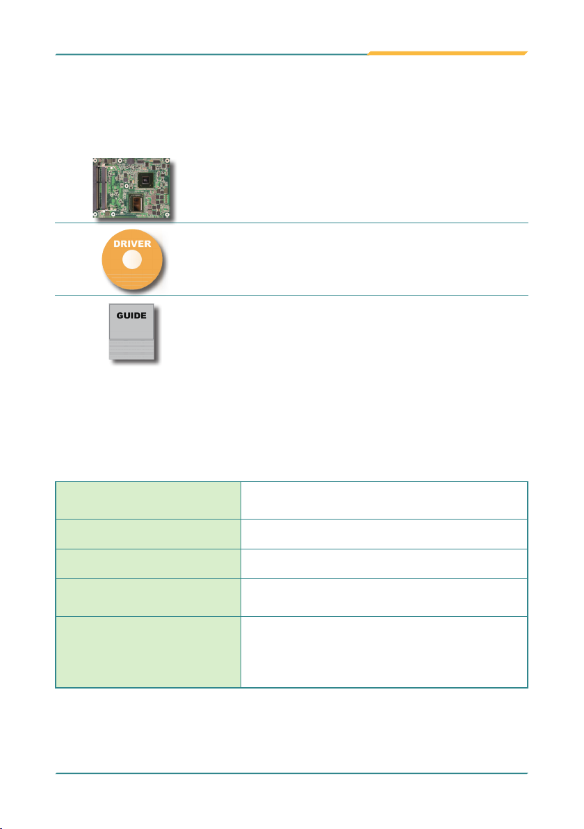
1.8 Packing List
Packing List
Before you begin installing your single board, please make sure that the following
materials have been shipped:
1 x COM-870E COM Express CPU Module
1 x Driver CD
1 x Quick Installation Guide
If any of the above items is damaged or missing, contact your vendor
immediately.
1.9 Ordering Information
COM-870E-827E
HS-65M2-F1 Heat Spreader (95 x 125 x 18mm)
HS-65M2-C1 Cooler (95 x 125 x 34.8mm)
PBE-1702
CBK-04-1702-00
Intel® Celeron 827E WT COM Express CPU
module
COM Express Type 6 evaluation board in
ATX form factor
Cable kit
1 x SATA cable
2 x COM port cables
1 x USB cable
- 6 -
Page 11

1.10 Specications
Introduction
Form Factor
CPU
Chipset
System Memory
VGA/ LCD
Controller
Ethernet controller
BIOS
Storage
Parallel Port
Universal Serial Bus
LCD
Expansion Interface
Operation Temp. -40ºC ~ 85ºC (-4ºF ~ 185ºF)
Watchdog Timer
Dimension (L x W)
COM Express Type 6 CPU Module
Intel® Celeron™ 827E 1.4GHz processor
Intel® HM65
2 x DDR3 SO-DIMM sockets, supporting up to 8GB
SDRAM
Intel® Graphics Media Accelerator 3000 graphics
core w/ Analog RGB/ Dual Channels 24-bit LVDS
(Dual independent displays), 3 x DDI ports
1 x Intel 82579LM Gigabit Ethernet PHY
AMI PnP Flash BIOS
2 x Serial ATA ports w/ 600MB/s HDD transfer rate
2 x Serial ATA ports w/ 300MB/s HDD transfer rate
SPP/EPP/ECP mode selectable (via COM Express
carrier board)
8 x USB 2.0 ports
Dual Channels 24-bit LVDS
1 x PCIe x16 lanes
5 x PCIe x1 lanes
SPI, and LPC (Low Pin Count) interface
1~ 255 levels Reset
125 x 95 mm (4.9” x 3.7”)
- 7 -
Page 12
Introduction
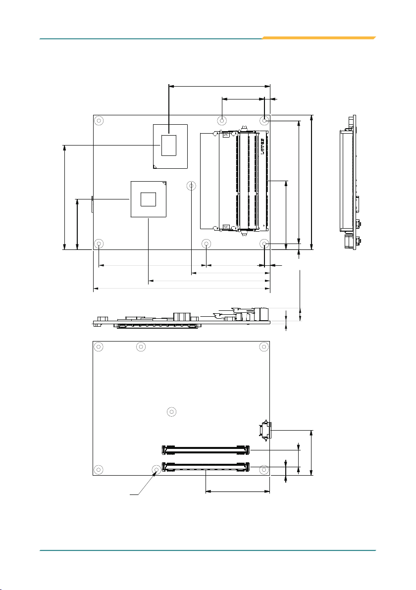
1.11 Board Dimensions
Sandy
Bridge
Processor
PCH
73,67
QM67
71,58
4,0030,00
95,00
87,00
35,56
Ø2.6*Ø6.5
125,00
86,01
55,68
45,35
48,46
4,00
41,0076,00
4,00
(9,2)
(SODIMM)
2
32
12
6
Unit: mm
- 8 -
Page 13

2Chapter 2
Installation
Installation
Chapter 2 - Installation
- 9 -
Page 14

Installation
2.1 What is “COM Express”?
With more and more demands on small and embedded industrial boards, a
multi-functioned COM (Computer-on-Module) is the great one of the
solutions.
COM Express, board-to-board connectors consist of two rows of 220 pins
each.
Row AB, which is required, provides pins for PCI Express, SATA, LVDS, LCD
channel, LPC bus, system and power management, VGA, LAN, and power
and ground interfaces.
Row CD, which is optional, provides SDVO and legacy PCI and IDE signals
next to additional PCI Express, LAN and power and ground signals.
By the way, the target markets of COM will be focused on:
● Retail & Advertising
● Medical
● Test & Measurement
● Gaming & Entertainment
● Industrial & Automation
● Military & Government
● Security
- 10 -
Page 15

Installation
COM Express supports seven pin-out Type applying to Basic and Extended
form factors:
Module Type 1 and 10 support single connector with two rows of pins (220
pins) Module Type 2, 3, 4, 5 and 6 support two connectors with four rows
of pins (440 pins) Connector placement and most mounting holes have
transparency between Form Factors.
The differences among the Module Type 6 and COM-870E are summarized
in table below:
Module Type Standard Type 6 COM-870E-827E
Connectors 2 2
Connector Rows A, B, C, D A, B, C, D
PCIe Lanes (Max) 24 23
PCI Bus No No
PATA - ID E No No
LAN (Max) 1 1
Serial Ports (Max) 2 0
Muxed SDVO No No
Digital Display I/F (Max) 3 3
USB 3.0 Ports (Max) 4 0
- 11 -
Page 16
Installation
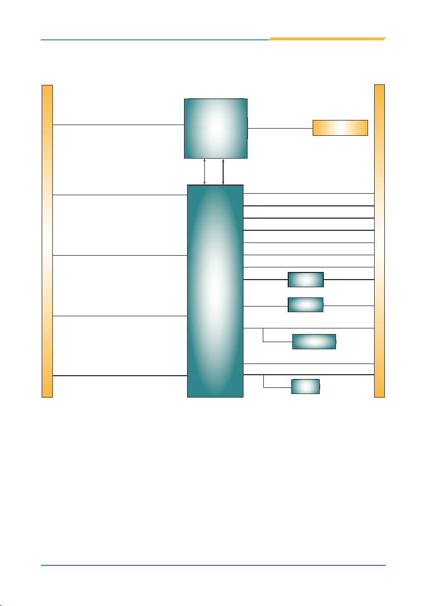
2.2 Block Diagram
PCIex16 (PEG)
DDI1 (DisplayPoer/HDMI/DIV/SDVO)
Connector CD
DDI2 (DisplayPort/HDMI/DVI)
Soldered
onboard
Intel®
Celeron 827E
Processor
DMI2
FDI
(x4)
Intel®
HM65
PCH
DDR3-1333/1066MHz
Dual Channels 24-bit LVDS
Analog RGB
HD Audio Link
SATA0, 1 (600Gb/s)
SATA2, 3 (300Gb/s)
USB Port 0 ~7
5 x PCIex1
Intel 82579LM
PCIex1
GbE controller
2 x SO-DIMM DDR3
sockets
GbE LAN
Connector AB
DDI3 (DisplayPort/HDMI/DVI)
1 x PCIex1
- 12 -
SMBus
LPC I/F
SPI Bus
Fintek
F75111
LPC I/F
TPM 1.2 (optional)
Infineon SLB9635
SMBus
SPI Bus
SPI BIOS
8 GPIO
Page 17
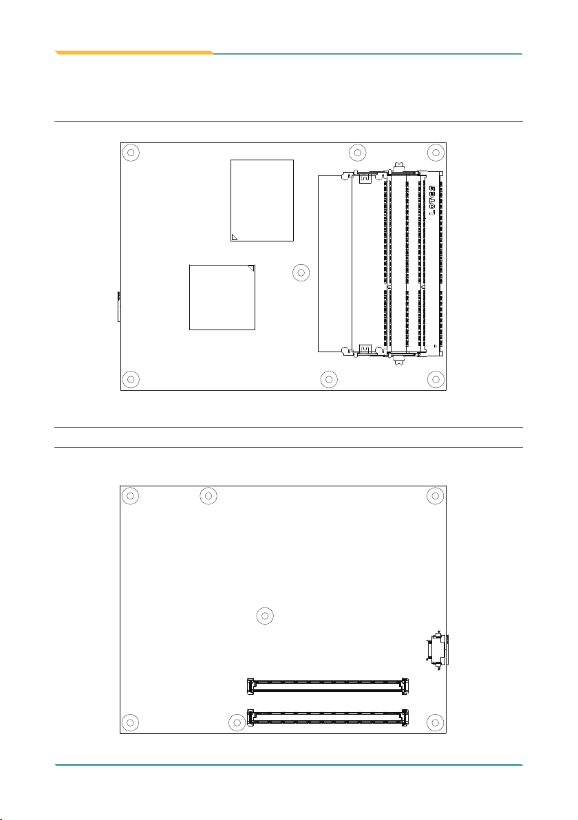
2.3 Connectors
Top side
Bottom side
COM Express AB Connector
COM Express CD Connector
Installation
Sandy
Bridge
Processor
PCH
QM67
COM Express CD Connector
COM Express AB Connector
- 13 -
Page 18

Installation
2.4 COM Express AB Connector (bottom side)
GND (FIXED)
B1
GBE0_ACT#
B2
LPC_FRAME#
B3
LPC_AD0
B4
LPC_AD1
B5
LPC_AD2
B6
LPC_AD3
B7
LPC_DRQ0#
B8
LPC_DRQ1#
B9
LPC_CLK
B10
GND (FIXED)
B11
PWRBTN#
B12
SMB_CK
B13
SMB_DAT
B14
SMB_ALERT#
B15
SATA1_TX+
B16
SATA1_TX-
B17
SUS_STAT#
B18
SATA1_RX+
B19
SATA1_RX-
B20
GND (FIXED)
B21
SATA3_TX+
B22
SATA3_TX-
B23
PWR_OK
B24
SATA3_RX+
B25
SATA3_RX-
B26
WDT
B27
AC_SDIN2
B28
AC_SDIN1
B29
AC_SDIN0
B30
GND
B31
SPKR
B32
I2C_CK
B33
I2C_DAT
B34
THRM#
B35
USB7-
B36
USB7+
B37
USB_4_5_OC#
B38
USB5-
B39
USB5+
B40
GND
B41
USB3-
B42
USB3+
B43
USB_0_1_OC#
B44
USB1-
B45
USB1+
B46
EXCD1_PERST#
B47
EXCD1_CPPE#
B48
SYS_RESET#
B49
CB_RESET#
B50
GND
B51
PCIE_RX5+
B52
PCIE_RX5-
B53
GPO1
B54
PCIE_RX4+
B55
GND (FIXED)
GBE0_MDI3-
GBE0_MDI3+
GBE0_LINK100#
GBE0_LINK1000#
GBE0_MDI2GBE0_MDI2+
GBE0_LINK#
GBE0_MDI1GBE0_MDI1+
GND (FIXED)
GBE0_MDI0GBE0_MDI0+
GBE0_CTREF
SUS_S3#
SATA0_TX+
SATA0_TX-
SUS_S4#
SATA0_RX+
SATA0_RX-
GND (FIXED)
SATA2_TX+
SATA2_TX-
SUS_S5#
SATA2_RX+
SATA2_RX-
BATLOW#
ATA_ACT#
AC_SYNC
AC_RST#
GND
AC_BITCLK
AC_SDOUT
BIOS_DISABLE#
THRMTRIP#
USB6-
USB6+
USB_6_7_OC#
USB4-
USB4+
GND
USB2-
USB2+
USB_2_3_OC#
USB0-
USB0+
VCC_RTC
EXCD0_PERST#
EXCD0_CPPE#
LPC_SERIRQ
GND
PCIE_TX5+
PCIE_TX5-
GPI0
PCIE_TX4+
A1
A2
A3
A4
A5
A6
A7
A8
A9
A10
A11
A12
A13
A14
A15
A16
A17
A18
A19
A20
A21
A22
A23
A24
A25
A26
A27
A28
A29
A30
A31
A32
A33
A34
A35
A36
A37
A38
A39
A40
A41
A42
A43
A44
A45
A46
A47
A48
A49
A50
A51
A52
A53
A54
A55
PCIE_RX4-
B56
GPO2
B57
PCIE_RX3+
B58
PCIE_RX3-
B59
GND
B60
PCIE_RX2+
B61
PCIE_RX2-
B62
GPO3
B63
PCIE_RX1+
B64
PCIE_RX1-
B65
WAKE0#
B66
WAKE1#
B67
PCIE_RX0+
B68
PCIE_RX0-
B69
GND
B70
LVDS_B0+
B71
LVDS_B0-
B72
LVDS_B1+
B73
LVDS_B1-
B74
LVDS_B2+
B75
LVDS_B2-
B76
LVDS_B3+
B77
LVDS_B3-
B78
LVDS_BKLT_EN
B79
GND
B80
LVDS_B_CK+
B81
LVDS_B_CK-
B82
CKLVDS_BKLT_CTRL
B83
VCC_5V_SBY
B84
VCC_5V_SBY
B85
VCC_5V_SBY
B86
VCC_5V_SBY
B87
RSVD
B88
VGA_RED
B89
GND
B90
VGA_GRN
B91
VGA_BLU
B92
VGA_HSYNC
B93
VGA_VSYNC
B94
VGA_I2C_CK
B95
VGA_I2C_DAT
B96
TV_DAC_A
B97
TV_DAC_B
B98
TV_DAC_C
B99
GND
B100
VCC_12V
B101
VCC_12V
B102
VCC_12V
B103
VCC_12V
B104
VCC_12V
B105
VCC_12V
B106
VCC_12V
B107
VCC_12V
B108
VCC_12V
B109
GND
B110
PCIE_TX4-
GND
PCIE_TX3+
PCIE_TX3-
GND
PCIE_TX2+
PCIE_TX2-
GPI1
PCIE_TX1+
PCIE_TX1-
GND
GPI2
PCIE_TX0+
PCIE_TX0-
GND
LVDS_A0+
LVDS_A0-
LVDS_A1+
LVDS_A1-
LVDS_A2+
LVDS_A2-
LVDS_VDD_EN
LVDS_A3+
LVDS_A3-
GND
LVDS_A_CK+
LVDS_A_CK-
LVDS_I2C_CK
LVDS_I2C_DAT
GPI3
KBD_RST#
KBD_A20GATE
PCIE0_CK_REF+
PCIE0_CK_REF-
GND
RSVD B91
RSVD
GPO0
RSVD
RSVD
GND
VCC_12V
VCC_12V
VCC_12V
GND
VCC_12V
VCC_12V
VCC_12V
VCC_12V
VCC_12V
VCC_12V
VCC_12V
VCC_12V
VCC_12V
GND
A56
A57
A58
A59
A60
A61
A62
A63
A64
A65
A66
A67
A68
A69
A70
A71
A72
A73
A74
A75
A76
A77
A78
A79
A80
A81
A82
A83
A84
A85
A86
A87
A88
A89
A90
A91
A92
A93
A94
A95
A96
A97
A98
A99
A100
A101
A102
A103
A104
A105
A106
A107
A108
A109
A110
- 14 -
Page 19

2.5 COM Express CD Connector (bottom side)
Installation
GND (FIXED)
D1
GND
D2
USB_SSTX0-
D3
USB_SSTX0+
D4
GND
D5
USB_SSTX1-
D6
USB_SSTX1+
D7
GND
D8
USB_SSTX2-
D9
USB_SSTX2+
D10
GND (FIXED)
D11
USB_SSTX3-
D12
USB_SSTX3+
D13
GND
D14
DDI1_CTRLCLK_AUX+
D15
DDI1_CTRLCLK_AUX-
D16
RSVD
D17
RSVD
D18
PCIE_TX6+
D19
PCIE_TX6-
D20
GND(FIXED)
D21
PCIE_TX7+
D22
PCIE_TX7-
D23
RSVD
D24
RSVD
D25
DDI1_PAIR0+
D26
DDI1_PAIR0-
D27
RSVD
D28
DDI1_PAIR1+
D29
DDI1_PAIR1-
D30
GND(FIXED)
D31
DDI1_PAIR2+
D32
DDI1_PAIR2-
D33
DDI1_DDC_AUX_SEL
D34
RSVD
D35
DDI1_PAIR3+
D36
DDI1_PAIR3-
D37
RSVD
D38
DDI1_PAIR0+
D39
DDI1_PAIR0-
D40
GND(FIXED)
D41
DDI1_PAIR1+
D42
DDI1_PAIR1-
D43
DDI2_HPD
D44
RSVD
D45
DDI2_PAIR2+
D46
DDI2_PAIR2-
D47
RSVD
D48
DDI2_PAIR3+
D49
DDI2_PAIR3-
D50
GND (FIXED)
D51
PEG_TX0+
D52
PEG_TX0-
D53
PEG_LANE_RV#
D54
PEG_TX1+
D55
GND (FIXED)
USB_SSRX0-
USB_SSRX0+
USB_SSRX1-
USB_SSRX1+
USB_SSRX2-
USB_SSRX2+
GND (FIXED)
USB_SSRX3-
USB_SSRX3+
DDI1_PAIR6+
DDI1_PAIR6-
PCIE_RX6+
PCIE_RX6-
GND(FIXED)
PCIE_RX7+
PCIE_RX7-
DDI1_PAIR4+
DDI1_PAIR4-
DDI1_PAIR5+
DDI1_PAIR5-
GND (FIXED)
DDI2_CTRLCLK_AUX+
DDI2_CTRLCLK_AUX-
DDI2_DDC_AUX_SEL
DDI3_CTRLCLK_AUX+
DDI3_CTRLCLK_AUX-
DDI3_DDC_AUX_SEL
DDI3_PAIR0+
DDI3_PAIR0-
GND(FIXED)
DDI3_PAIR1+
DDI3_PAIR1-
DDI3_PAIR2+
DDI3_PAIR2-
DDI3_PAIR3+
DDI3_PAIR3-
GND (FIXED)
PEG_RX0+
PEG_RX1+
GND
GND
GND
GND
RSVD
RSVD
DDI1_HPD
RSVD
RSVD
RSVD
DDI3_HPD
RSVD
RSVD
PEG_RX0-
TYPE0#
C1
C2
C3
C4
C5
C6
C7
C8
C9
C10
C11
C12
C13
C14
C15
C16
C17
C18
C19
C20
C21
C22
C23
C24
C25
C26
C27
C28
C29
C30
C31
C32
C33
C34
C35
C36
C37
C38
C39
C40
C41
C42
C43
C44
C45
C46
C47
C48
C49
C50
C51
C52
C53
C54
C55
D56
D57
D58
D59
D60
D61
D62
D63
D64
D65
D66
D67
D68
D69
D70
D71
D72
D73
D74
D75
D76
D77
D78
D79
D80
D81
D82
D83
D84
D85
D86
D87
D88
D89
D90
D91
D92
D93
D94
D95
D96
D97
D98
D99
D100
D101
D102
D103
D104
D105
D106
D107
D108
D109
D110
PEG_TX1TYPE2#
PEG_TX2+
PEG_TX2GND (FIXED)
PEG_TX3+
PEG_TX3RSVD
RSVD
PEG_TX4+
PEG_TX4RSVD
PEG_TX5+
PEG_TX5GND (FIXED)
PEG_TX6+
PEG_TX6GND
PEG_TX7+
PEG_TX7GND
RSVD
PEG_TX8+
PEG_TX8GND (FIXED)
PEG_TX9+
PEG_TX9RSVD
GND
PEG_TX10+
PEG_TX10GND
PEG_TX11+
PEG_TX11GND (FIXED)
PEG_TX12+
PEG_TX12GND
PEG_TX13+
PEG_TX13GND
RSVD
PEG_TX14+
PEG_TX14GND (FIXED)
PEG_TX15+
PEG_TX15GND
VCC_12V
VCC_12V
VCC_12V
VCC_12V
VCC_12V
VCC_12V
GND (FIXED)
PEG_RX1-
TYPE1#
PEG_RX2+
PEG_RX2-
GND (FIXED)
PEG_RX3+
PEG_RX3-
RSVD
RSVD
PEG_RX4+
PEG_RX4-
RSVD
PEG_RX5+
PEG_RX5-
GND (FIXED)
PEG_RX6+
PEG_RX6-
GND
PEG_RX7+
PEG_RX7-
GND
RSVD
PEG_RX8+
PEG_RX8-
GND (FIXED)
PEG_RX9+
PEG_RX9-
RSVD
GND
PEG_RX10+
PEG_RX10-
GND
PEG_RX11+
PEG_RX11-
GND (FIXED)
PEG_RX12+
PEG_RX12-
GND
PEG_RX13+
PEG_RX13-
GND
RSVD
PEG_RX14+
PEG_RX14-
GND (FIXED)
PEG_RX15+
PEG_RX15-
GND
VCC_12V
VCC_12V
VCC_12V
VCC_12V
VCC_12V
VCC_12V
GND (FIXED)
C56
C57
C58
C59
C60
C61
C62
C63
C64
C65
C66
C67
C68
C69
C70
C71
C72
C73
C74
C75
C76
C77
C78
C79
C80
C81
C82
C83
C84
C85
C86
C87
C88
C89
C90
C91
C92
C93
C94
C95
C96
C97
C98
C99
C100
C101
C102
C103
C104
C105
C106
C107
C108
C109
C110
- 15 -
Page 20

Installation
2.6 The Installation Paths of CD Driver
Windows 2000 & XP
Driver Path
CHIPSET \EmETXe-i67M2\CHIPSET
LAN
NET Framework \EmETXe-i67M2\NET Framework
VGA
Management
Engine
RAID \EmETXe-i67M2\IRST
\EmETXe-i67M2\ETHERNET\XP_WIN7_SERIES\32
\EmETXe-i67M2\ETHERNET\XP_WIN7_SERIES\64
\EmETXe-i67M2\GRAPHICS\Windows XP 32bit
Graphics Drivers\Windows XP Graphics Drivers\
winxp
\EmETXe-i67M2\GRAPHICS\Windows XP 64bit
Graphics Drivers\Windows XP64 Graphics Drivers\
winxp64
\EmETXe-i67M2\ME
Windows 7
Driver Path
CHIPSET \EmETXe-i67M2\CHIPSET
LAN
VGA
Management
Engine
Intel Turbo \EmETXe-i67M2\OTHERS
\EmETXe-i67M2\ETHERNET\XP_WIN7_SERIES\32
\EmETXe-i67M2\ETHERNET\XP_WIN7_SERIES\64
\EmETXe-i67M2\GRAPHICS\Windows 7 Graphics
Driver 32_bit\Windows Vista Windows 7 Graphics
Driver\WinVista7
\EmETXe-i67M2\GRAPHICS\Windows 7 64-Bit
Graphics Driver\Windows Vista Windows 7 64-Bit
Graphics Driver\WinVista7_64
\EmETXe-i67M2\ME
- 16 -
Page 21
Installation
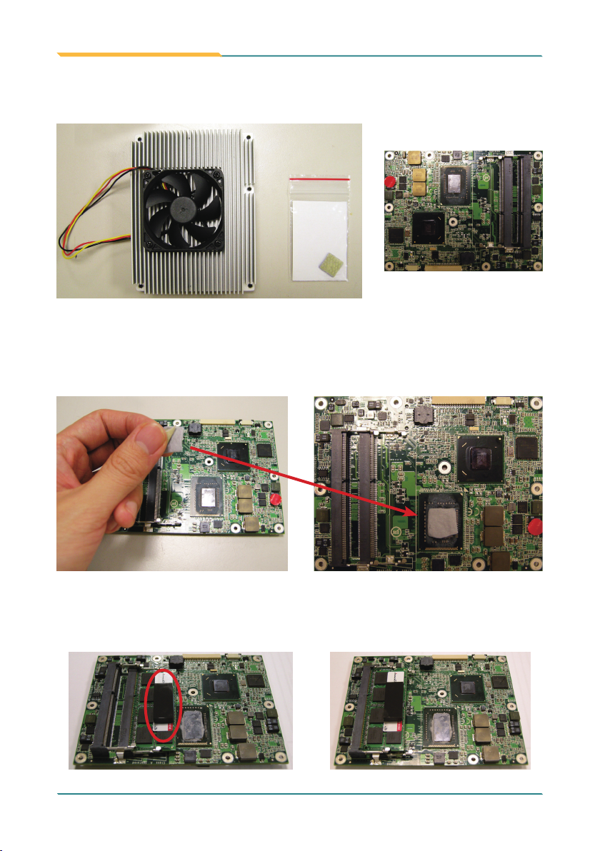
2.7 Heatsink Installation
1. Prepare your optional heatsink, thermal pad and CPU module.
2. You have to put an additional thermal pad between heatsink and CPU
module. Please tear protective membranes on both sides from thermal pad
rst of all, be sure not to pinch or mold the thermal pad, and then put it as
right picture.
3. You may also apply thermal pad to their memory module. But be aware to
put it on the designated place of the rst module, as the left illustration, and
don’t put it on the 2nd module, as right picture, for the 2nd memory module
doesn’t need it.
(O) (X)
- 17 -
Page 22
Installation
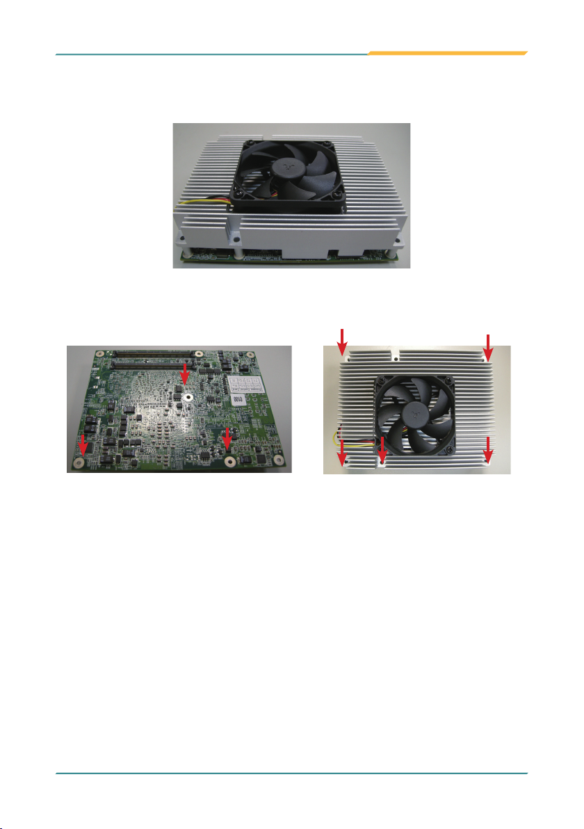
4. After everything is settled down, please assemble heatsink with CPU
module according to their corresponding screw positions.
5. Carefully turn them over together and secure the rst 3 screws as left
picture. Overturn again to secure the rest as right picture.
- 18 -
Page 23

BIOS
BIOS
3Chapter 3
Chapter 3 - BIOS
- 19 -
Page 24

BIOS
3.1 BIOS Main Setup
The AMI BIOS provides a setup utility program for specifying the system
congurations and settings which are stored in the BIOS ROM of the system.
When you turn on the computer, the AMI BIOS is immediately activated. After
you have entered the setup utility, use the left/right arrow keys to highlight a
particular conguration screen from the top menu bar or use the down arrow
key to access and congure the information below.
NOTE: In order to increase system stability and performance, our engineering
staff are constantly improving the BIOS menu. The BIOS setup screens and
descriptions illustrated in this manual are for your reference only, and may not
completely match what you see on your screen.
BIOS Information
Display the BIOS information.
- 20 -
Page 25

BIOS
System Date
Set the system date. Note that the ‘Day’ automatically changes when you set
the date.
The date format is: Day : Sun to Sat
Month : 1 to 12
Date : 1 to 31
Year : 1999 to 2099
System Time
Set the system time.
The time format is: Hour : 00 to 23
Minute : 00 to 59
Second : 00 to 59
3.2 Advanced Settings
Legacy OpROM Support
Launch PXE OpROM
Enable or disable the boot option for legacy network devices.
Launch Storage OpROM
Enable or Disable Boot Option for Legacy Mass Storage Devices with Option
ROM.
- 21 -
Page 26

BIOS
3.2.1 ACPI Conguration
Enable Hibernation
Enable or disable System ability to Hibernation (OS/S4 Sleep State). This option may be not effective with some OS.
ACPI Sleep State
Select the highest ACPI sleep state the system will enter when the SUSPEND
button is pressed.
The choice: Suspend Disabled, S1 (CPU Stop Clock), S3 (Suspend to RAM)
Lock Legacy Resources
Enable or disable Lock of Legacy Resources.
Power-Supply Type
Set power-supply type.
The choice: AT, ATX
- 22 -
Page 27

BIOS
3.2.2 CPU Conguration
The CPU Conguration setup screen varies depending on the installed
processor.
Hyper-threading
This item is used to enable or disable the processor’s Hyper-threading
feature.
Enabled for Windows XP and Linux (OS optimized for Hyper-threading
Technology) and disabled for other OS (OS not optimized for Hyper-threading
Technology).
When disabled, only one thread per enabled core is enabled.
Limit CPUID Maximum
Enable or disable the Limit CPUID Maximum.
Intel Virtualization Technology
When enabled, a VMM can utilize the additional hardware capabilities provided by Vanderpool Technology.
- 23 -
Page 28

BIOS
3.2.3 SATA Conguration
It allows you to select the operation mode for SATA controller.
SATA Controller(s)
Enable or disable SATA devices.
SATA Mode Selection
The choice: Disable; IDE (Default), RAID
IDE: Set the Serial ATA drives as Parallel ATA storage devices.
RAID: Create RAID or Intel Matrix Storage conguration on Serial ATA
devices.
- 24 -
Page 29

3.2.4 Intel Anti-Theft Technology Conguration
BIOS
Intel Anti-Theft Technology
Enable or disable Intel® Anti-Theft Technology function in BIOS.
Intel Anti-Theft Technology Recovery
Set the number of times Recovery attempted will be allowed.
Enter Intel AT Suspend Mode
Enable or disable the request that platform enters AT suspend mode.
- 25 -
Page 30

BIOS
3.2.5 AMT Conguration
BIOS Hotkey Pressed
OEMFLag Bit 1:
Enable/Disable BIOS hotkey press.
MeBx Selection Screen
OEMFLag Bit 2:
Enable/Disable MEBx selection screen.
Verbose Mebx Output
OEMFLag Bit 3:
Enable/Disable Verbose Mebx Output.
- 26 -
Page 31

Hide Un-Congure ME Conrmation
OEMFLag Bit 6:
Hide Un-Congure ME without password Conrmation Prompt.
MeBx Debug Message Output
OEMFLag Bit 14:
Enable MEBx debug message output.
Un-Congure ME
OEMFLag Bit 15:
Un-Congure ME without password.
Intel AMT Password Write Enabled
Enable/Disable Intel AMT Password Write. Password is writable when
set Enable.
Amt Wait Timer
Set timer to wait before sending ASF_GET_BOOT_OPTIONS.
ASF
Enable/Disable Alert Specication Format.
Activate Remote Assistance Process
BIOS
Trigger CIRA boot.
USB Congure
Enable/Disable USB Congure function.
PET Progress
User can enable/disable PET Events progress to received PET events or
not.
Intel Amt SPI Protected
Enable/Disable Intel AMT SPI write protect.
WatchDog
Enable/Disable WatchDog Timer.
- 27 -
Page 32

BIOS
3.2.6 USB Conguration
Legacy USB Support
Enable support for legacy USB. AUTO option disables legacy support if no
USB devices are connected.
The choice: Enabled (Default); Auto; Disabled
EHCI Hand-off
Allow you to enable support for operating systems without an EHCI hand-off
feature. Do not disable the BIOS EHCI Hand-Off option if you are running a
Windows® operating system with USB device.
The choice: Enabled (Default); Disabled
USB Beep Switch
Enable/Disable USB Beep sound.
- 28 -
Page 33

BIOS
USB hardware delays and time-outs
USB transfer time-out — The time-out value for control, bulk, and interrupt
transfers. Default setting: 20 sec
Device reset time-out — USB mass storage device start unit command timeout. Default setting: 20 sec
Device power-up delay — Maximum time the device will take before it properly reports itself to the host controller. ‘Auto’ uses default value: for a Root
port it is 100ms, for a Hub port the delay is taken from hub descriptor. The
choice: Auto (Default); Manual
Mass Storage Devices
This item displays information when USB devices are detected.
3.2.7 H/W Monitor
PC Health Status
The hardware monitor menu shows the operating temperature and system
voltages of CPU module.
- 29 -
Page 34

BIOS
3.2.8 Super IO Conguration
You can use this item to set up or change the Super IO conguration for FDD
controllers, parallel ports and serial ports.
Power On After Power Failure
Specify what state to go to when power is re-applied after a power failure.
- 30 -
Page 35

BIOS
Serial Port 1~2 Conguration
Serial Port
Use the Serial port option to enable or disable the serial port.
The choice: Enabled, Disabled
Change Settings
Use the Change Settings option to change the serial port’s IO port address
and interrupt address.
The choice:
Auto
IO=3F8h; IRQ=4,
IO=3F8h; IRQ=3,4,5,6,7,10,11,12
IO=2F8h; IRQ=3,4,5,6,7,10,11,12
IO=3E8h; IRQ=3,4,5,6,7,10,11,12
IO=2E8h; IRQ=3,4,5,6,7,10,11,12
- 31 -
Page 36

BIOS
Parallel Port Conguration
Parallel Port Conguration
This item allows you to enable/disable Parallel Port (LPT/LPTE).
Change Settings
Use the Change Settings option to change the parallel port’s IO port address
and interrupt address.
The choice:
Auto
IO=378h; IRQ=5,
IO=378h; IRO=5,6,7,10,11,12,
IO=378h; IRQ=5,6,7,10,11,12,
IO=278h; IRQ=5,6,7,10,11,12,
IO=38Ch; IRQ=5,6,7,10,11,12,
Device Mode
The choice: Standard Parallel Port Mode, EPP Mode, ECP Mode, EPP Mode
& ECP Mode.
- 32 -
Page 37

3.2.9 Sandybridge PPM Conguration
EIST
Enable/Disable Intel SpeedStep.
CPU C3 Report
Enable/Disable CPU C3(ACPI C2) report to OS.
CPU C6 Report
Enable/Disable CPU C6(ACPI C3) report to OS.
CPU C7 Report
Enable/Disable CPU C7(ACPI C3) report to OS.
Long duration power limit
Long duration power limit in Watts, 0 means use factory default.
Long duration maintained
Time window which the long duration power is maintained.
Short duration power limit
Short duration power limit in Watts, 0 means use factory default.
TCC active offset
Offset from the factory TCC activation temperature.
BIOS
- 33 -
Page 38

BIOS
3.3 Chipset
This section allows you to congure and improve your system; also, set up
some system features according to your preference.
- 34 -
Page 39

3.3.1 System Agent (SA) Conguration
CHAP Device (B0:D7:F0)
Enable or disable SA CHAP Device.
Thermal Device (B0:D4 F0)
Enable or disable SA Thermal Device.
Enable NB CRID
Enable or disable NB CRID WorkAround.
BIOS
- 35 -
Page 40

BIOS
Graphics Conguration
Primary Display
Select which of IGFX/PEG/PCI Graphics Devices should be Primary Display
or select SG for Switchable Gfx.
Internal Graphics
Keep IGD enabled based on the option.
GTT Size
Select the GTT Size: 1MB, 2MB.
Aperture Size
Select the Aperture Size: 128MB, 256MB, 512MB.
DVMT Pre-Allocated
Select DVMT 5.0 Pre-Allocated (Fixed) Graphics Memory size used by the
Internal Graphics Device: 0M~512M.
DVMT Total Gfx Mem
Select DVMT5.0 Total Graphic Memory size used by the Internal Graphics
Device: 128M, 256M, MAX.
- 36 -
Page 41

Gfx Low Power Mode
This option is applicable for SFF only.
LCD Control
BIOS
Primary IGFX Boot Display
Select the Video Device which will be activated during POST. This has no effect if external graphics present.
Secondary boot display selection will appear based on your selection.
VGA modes will be supported only on primary display.
LCD Panel Type
Select LCD panel used by Internal Graphics Device by selecting the appropriate setup item: VBIOS Default, 640x480 LVDS ~ 2048x1536 LVDS.
Panel Scaling
Select the LCD panel scaling option used by the Internal Graphics Device:
Auto, Off, Force Scaling.
- 37 -
Page 42

BIOS
Backlight Control
The choice: PWM Inverted (Default), PWM Normal, GMBus Inverted and GMBus Normal.
BIA
The choice: VBIOS Default, Disabled and Level 1/2/3/4/5.
Spread Spectrum clock Chip
The default setting is Off. Other options are:
Hardware: Spread is controlled by chip.
Software: Spread is controlled by BIOS.
Active LFP
Select the Active LFP Conguration.
No LVDS: VBIOS does not enable LVDS.
Int-LVDS: VBIOS enables LVDS driver by Integrated encoder.
SDVO LVDS: VBIOS enables LVDS driver by SDVO encoder.
eDP Port-A: LFP driven by Int-DisplayPort encoder from Port-A.
Panel Color Depth
Select the LFP panel color depth: 18 Bit, 24 Bit.
- 38 -
Page 43

DMI Conguration
Control various DMI functions.
BIOS
DMI Vc1/Vcp/Vcm Control
Enable or disable DMI Vc1/Vcp/Vcm.
DMI Link ASPM Control
Enable or disable the control of Active State Power Management on SA side
of the DMI Link.
The choice: Disabled, L0s, L1, L0sL1
DMI Extended Synch Control
Enable or disable DMI Extended Synchronization.
DMI Gen 2
Enable or disable DMI Gen 2.
- 39 -
Page 44

BIOS
NB PCIe Conguration
Congure NB PCIe Express Settings.
PEG0 – Gen X
Congure PEG0 B0:D1:F0 Gen1-Gen2.
The choice: Auto, Gen1, Gen2
PEG1 – Gen X
Congure PEG1 B0:D1:F1 Gen1-Gen2.
The choice: Auto, Gen1, Gen2
PEG2 – Gen X
Congure PEG2 B0:D1:F2 Gen1-Gen2.
The choice: Auto, Gen1, Gen2
PEG3 – Gen X
Congure PEG3 B0:D6:F0 Gen1-Gen2.
The choice: Auto, Gen1, Gen2
Always Enable PEG
Enable the PEG slot.
- 40 -
Page 45

BIOS
PEG ASPM
Control ASPM support for the PEG Device. This has no effect if PEG is not the
currently active device.
The choice: Disabled, Auto, ASPM L0s, ASPM L1, ASPM L0sL1
De-emphasis Control
Congure the De-emphasis control on PEG.
The choice: -6 dB, -3.5 dB
Memory Conguration
DIMM prole
Select DIMM timing prole that should be used.
The choice: Default DIMM prole, XMP prole 1, XMP prole 2
Memory Frequency
Maximum Memory Frequency Selections in Mhz.
The choice: Auto, 1067, 1333, 1600, 1867, 2133
ECC Support
Enable or disable DDR Ecc Support.
- 41 -
Page 46

BIOS
Max TOLUD
Maximum Value of TOLUD. Dynamic assignment would adjust TOLUD
automatically based on largest MMIO length of installed graphic controller.
The choice: Dynamic, 1GB, 1.25 GB, 1.5 GB, 1.75 GB, 2GB, 2.25 GB,
2.5 GB, 2.75 GB, 3 GB, 3.25 GB
NMode Support
NMode Support Option.
The choice: Auto, 1 N Mode, 2 N Mode
Memory Scrambler
Enable or disable Memory Scrambler support.
RMT Crosser Support
Enable or disable RmtCrosserEnable support.
MRC Fast Boot
Enable or disable MRC fast boot.
Force Cold Reset
Force cold reset or choose MRC cold reset mode, when cold boot is required
during MRC execution.
NOTE: If ME 5.0MB is present, Force cold reset is required!
Scrambler Seed Generation Off
Control Memory Scrambler Seed Generation.
Enable - do not generate scrambler seed.
Disable - generate scrambler seed always.
Memory Remap
Enable or disable memory remap above 4G.
Channel A DIMM Control
Enable or disable dimms on channel A.
- 42 -
Page 47

Memory Thermal Conguration
Memory Thermal Conguration Options.
BIOS
Memory Thermal Management
Enable or disable Memory Thermal Management.
PECI Injected Temperature
Enable or disable memory temperatures to be injected to the processor via
PECI.
EXTT# via TS-on-Board
Enable or disable routing TS-on-Board’s ALERT# and THERM# to EXTTS#
pins on the PCH.
EXTT# via TS-on-DIMM
Enable or disable routing TS-on-DIMM’s ALERT# to EXTTS# pin on the PCH.
Virtual Temperature Sensor (VTS)
Enable or disable Virtual Temperature Sensor.
- 43 -
Page 48

BIOS
GT – Power Management Control
RC6 (Render Standby)
Check to enable render standby support.
GT Overclocking Support
Enable or disable GT Overclocking Support.
- 44 -
Page 49

3.3.2 PCH-IO Conguration
BIOS
PCIE Wake UP
Enable or disable PCIE Wake# to wake the system.
Wake on RING
Enable or disable Wake on RING (WOR). Computer will start up simply by applying power to a connected external modem if WOR is enabled.
Azalia
Control detection of the Azalia device.
Disabled = Azalia will be unconditionally disabled.
Enabled = Azalia will be unconditionally enabled.
Auto = Azalia will be enabled if present, disabled otherwise.
SLP_S4 Assertion Width
Select a minimum assertion width of the SLP_S4# signal.
The choice: 1-2 Seconds, 2-3 Seconds, 3-4 Seconds, 4-5 Seconds
Restore AC Power Loss
Select AC power state when power is re-applied after a power failure.
- 45 -
Page 50

BIOS
USB Conguration
EHCI1~2
Control the USB EHCI (USB2.0) functions.
One EHCI controller must always be enabled.
USB Ports Per-Port Disable Control
Enable or disable each of the USB ports (0~9).
- 46 -
Page 51

PCI Express Conguration
BIOS
PCI Express Clock Gating
Enable or disable PCI Express Clock Gating for each root port.
DMI Link ASPM Control
The control of Active State Power Management on both NB side and SB
side of the DMI Link.
DMI Link Extended Synch Control
The control of Extended Synch on SB side of the DMI Link.
Subtractive Decode
Enable or disable Subtractive Decode.
- 47 -
Page 52

BIOS
PCI Express Root Port 1~8
PCI Express Root Port 1~8
Control the PCI Express Root Port.
PEG1 – Gen X
Congure PEG1 B0 :D1 :F1 Gen1-Gen2
The choice: Auto, Gen1, Gen2
ASPM Support
Set the ASPM Level to Disabled, L0s, L1, L0sL1, Auto
Force L0 - Force all links to L0 State
AUTO - BIOS auto conguration
DISABLE - Disable ASPM
- 48 -
Page 53

BIOS
URR
Enable or disable PCI Express Unsupported Request Reporting.
FER
Enable or disable PCI Express Device Fatal Error Reporting.
NFER
Enable or disable PCI Express Device Non-Fatal Error Reporting.
CER
Enable or disable PCI Express Device Correctable Error Reporting.
CTO
Enable or disable PCI Express Completion Timer TO.
SEFE
Enable or disable Root PCI Express System Error on Fatal Error.
SENFE
Enable or disable Root PCI Express System Error on Non-Fatal Error.
SECE
Enable or disable Root PCI Express System Error on Correctable Error.
PME SCI
Enable or disable PCI Express PME SCI.
Hot Plug
Enable or disable PCI Express Hot Plug.
Extra Bus Reserved
Extra Bus Reserved (0-7) for bridges behind this Root Bridge.
Reserved Memory
Reserved Memory and Prefetchable Memory (1-20MB) Range for this Root
Bridge.
Reserved I/O
Reserved I/O (4k/8k/12k/16k/20k) Range for this Root Bridge.
- 49 -
Page 54

BIOS
3.4 Boot Settings
The Boot menu items allow you to change the system boot options.
Boot Conguration
Bootup NumLock State
This setting determines whether the Num Lock key should be activated at
boot up.
Quiet Boot
This allows you to select the screen display when the system boots.
Boot Option Priorities
Select the boot sequence of the hard drives.
Hard Drive BBS Priorities
This allows you to set the hard drive boot priority. The BIOS will attempt to
arrange the hard disk boot sequence automatically. You can also change the
booting sequence. The number of device items that appears on the screen
depends on the number of devices installed in the system.
- 50 -
Page 55

3.5 Security
BIOS
Administrator Password
Use the Administrator Password to set or change a administrator password.
ENTER PASSWORD
Type the password, up to eight characters in length, and press <Enter>. The
password typed now will clear any previously entered password from CMOS
memory. You will be asked to conrm the password. Type the password again
and press <Enter>. You may also press <ESC> to abort the selection and not
enter a password.
To disable a password, just press <Enter> when you are prompted to enter
the password. A message will conrm the password will be disabled. Once
the password is disabled, the system will boot and you can enter Setup freely.
PASSWORD DISABLED
When a password has been enabled, you will be prompted to enter it every
time you try to enter Setup. This prevents an unauthorized person from
- 51 -
Page 56

BIOS
changing any part of your system conguration.
Additionally, when a password is enabled, you can also require the BIOS to
request a password every time your system is rebooted. This would prevent
unauthorized use of your computer.
You can determine when the password is required within the BIOS Features
Setup Menu and its Security option. If the Security option is set to “System”,
the password will be required both at boot and at entry to Setup. If it’s set to
“Setup”, prompting only occurs when trying to enter Setup.
- 52 -
Page 57

3.6 Save & Exit
Save Changes and Reset
Pressing <Enter> on this item and it asks for conrmation:
Save conguration changes and exit setup?
BIOS
Pressing <OK> stores the selection made in the menus in CMOS - a special
section of memory that stays on after you turn your system off. The next
time you boot your computer, the BIOS congures your system according to
the Setup selections stored in CMOS. After saving the values the system is
restarted again.
Restore Defaults
Restore system to factory default.
Pressing <Enter> on this item and it asks for conrmation prior to executing
this command.
Boot Override
This group of functions includes a list of tokens, each of them corresponding
to one device within the boot order. Select a drive to immediately boot that
device regardless of the current boot order.
- 53 -
Page 58

BIOS
3.7 AMI BIOS Checkpoints
3.7.1 Checkpoint Ranges
Status Code Range Description
0x01 – 0x0B SEC execution
0x0C – 0x0F SEC errors
0x10 – 0x2F
0x30 – 0x4F PEI execution after memory detection
0x50 – 0x5F PEI errors
0x60 – 0x8F DXE execution up to BDS
0x90 – 0xCF BDS execution
0xD0 – 0xDF DXE errors
0xE0 – 0xE8 S3 Resume (PEI)
0xE9 – 0xEF S3 Resume errors (PEI)
0xF0 – 0xF8 Recovery (PEI)
0xF9 – 0xFF Recovery errors (PEI)
PEI execution up to and including memory
detection
- 54 -
Page 59

3.7.2 Standard Checkpoints
SEC Phase
Status Code Description
0x00 Not used
Progress Codes
0x01 Power on. Reset type detection (soft/hard).
0x02 AP initialization before microcode loading
0x03 North Bridge initialization before microcode loading
0x04 South Bridge initialization before microcode loading
0x05 OEM initialization before microcode loading
0x06 Microcode loading
0x07 AP initialization after microcode loading
0x08 North Bridge initialization after microcode loading
0x09 South Bridge initialization after microcode loading
0x0A OEM initialization after microcode loading
0x0B Cache initialization
SEC Error Codes
0x0C – 0x0D Reserved for future AMI SEC error codes
0x0E Microcode not found
0x0F Microcode not loaded
BIOS
- 55 -
Page 60

BIOS
PEI Phase
Status Code Description
Progress Codes
0x10 PEI Core is started
0x11 Pre-memory CPU initialization is started
0x12 Pre-memory CPU initialization (CPU module specic)
0x13 Pre-memory CPU initialization (CPU module specic)
0x14 Pre-memory CPU initialization (CPU module specic)
0x15 Pre-memory North Bridge initialization is started
0x16
0x17
0x18
0x19 Pre-memory South Bridge initialization is started
0x1A
0x1B
0x1C
0x1D – 0x2A OEM pre-memory initialization codes
0x2B
0x2C Memory initialization. Memory presence detection
0x2D
0x2E Memory initialization. Conguring memory
0x2F Memory initialization (other).
0x30 Reserved for ASL (see ASL Status Codes section below)
0x31 Memory Installed
Pre-Memory North Bridge initialization (North Bridge
module specic)
Pre-Memory North Bridge initialization (North Bridge
module specic)
Pre-Memory North Bridge initialization (North Bridge
module specic)
Pre-memory South Bridge initialization (South Bridge
module specic)
Pre-memory South Bridge initialization (South Bridge
module specic)
Pre-memory South Bridge initialization (South Bridge
module specic)
Memory initialization. Serial Presence Detect (SPD) data
reading
Memory initialization. Programming memory timing
information
- 56 -
Page 61

0x32 CPU post-memory initialization is started
0x33 CPU post-memory initialization. Cache initialization
0x34
0x35
0x36
0x37 Post-Memory North Bridge initialization is started
0x38
0x39
0x3A
0x3B Post-Memory South Bridge initialization is started
0x3C
0x3D
0x3E
0x3F-0x4E OEM post memory initialization codes
0x4F DXE IPL is started
PEI Error Codes
0x50
0x51 Memory initialization error. SPD reading has failed
0x52
0x53 Memory initialization error. No usable memory detected
0x54 Unspecied memory initialization error.
CPU post-memory initialization. Application Processor(s)
(AP) initialization
CPU post-memory initialization. Boot Strap Processor
(BSP) selection
CPU post-memory initialization. System Management
Mode (SMM) initialization
Post-Memory North Bridge initialization (North Bridge
module specic)
Post-Memory North Bridge initialization (North Bridge
module specic)
Post-Memory North Bridge initialization (North Bridge
module specic)
Post-Memory South Bridge initialization (South Bridge
module specic)
Post-Memory South Bridge initialization (South Bridge
module specic)
Post-Memory South Bridge initialization (South Bridge
module specic)
Memory initialization error. Invalid memory type or
incompatible memory speed
Memory initialization error. Invalid memory size or
memory modules do not match.
BIOS
- 57 -
Page 62

BIOS
0x55 Memory not installed
0x56 Invalid CPU type or Speed
0x57 CPU mismatch
0x58 CPU self test failed or possible CPU cache error
0x59
0x5A Internal CPU error
0x5B reset PPI is not available
0x5C-0x5F Reserved for future AMI error codes
S3 Resume Progress Codes
0xE0
0xE1 S3 Boot Script execution
0xE2 Video repost
0xE3 OS S3 wake vector call
0xE4-0xE7 Reserved for future AMI progress codes
S3 Resume Error Codes
0xE8 S3 Resume Failed
0xE9 S3 Resume PPI not Found
0xEA S3 Resume Boot Script Error
0xEB S3 OS Wake Error
0xEC-0xEF Reserved for future AMI error codes
Recovery Progress Codes
0xF0 Recovery condition triggered by rmware (Auto recovery)
0xF1 Recovery condition triggered by user (Forced recovery)
0xF2 Recovery process started
0xF3 Recovery rmware image is found
0xF4 Recovery rmware image is loaded
0xF5-0xF7 Reserved for future AMI progress codes
Recovery Error Codes
0xF8 Recovery PPI is not available
CPU micro-code is not found or micro-code update is
failed
S3 Resume is stared (S3 Resume PPI is called by the
DXE IPL)
- 58 -
Page 63

0xF9 Recovery capsule is not found
0xFA Invalid recovery capsule
0xFB – 0xFF Reserved for future AMI error codes
DXE Phase
Status Code Description
0x60 DXE Core is started
0x61 NVRAM initialization
0x62 Installation of the South Bridge Runtime Services
0x63 CPU DXE initialization is started
0x64 CPU DXE initialization (CPU module specic)
0x65 CPU DXE initialization (CPU module specic)
0x66 CPU DXE initialization (CPU module specic)
0x67 CPU DXE initialization (CPU module specic)
0x68 PCI host bridge initialization
0x69 North Bridge DXE initialization is started
0x6A North Bridge DXE SMM initialization is started
0x6B
0x6C
0x6D
0x6E
0x6F
0x70 South Bridge DXE initialization is started
0x71 South Bridge DXE SMM initialization is started
0x72 South Bridge devices initialization
0x73
North Bridge DXE initialization (North Bridge module
specic)
North Bridge DXE initialization (North Bridge module
specic)
North Bridge DXE initialization (North Bridge module
specic)
North Bridge DXE initialization (North Bridge module
specic)
North Bridge DXE initialization (North Bridge module
specic)
South Bridge DXE Initialization (South Bridge module
specic)
BIOS
- 59 -
Page 64

BIOS
0x74
0x75
0x76
0x77
0x78 ACPI module initialization
0x79 CSM initialization
0x7A – 0x7F Reserved for future AMI DXE codes
0x80 – 0x8F OEM DXE initialization codes
0x90 Boot Device Selection (BDS) phase is started
0x91 Driver connecting is started
0x92 PCI Bus initialization is started
0x93 PCI Bus Hot Plug Controller Initialization
0x94 PCI Bus Enumeration
0x95 PCI Bus Request Resources
0x96 PCI Bus Assign Resources
0x97 Console Output devices connect
0x98 Console input devices connect
0x99 Super IO Initialization
0x9A USB initialization is started
0x9B USB Reset
0x9C USB Detect
0x9D USB Enable
0x9E – 0x9F Reserved for future AMI codes
0xA0 IDE initialization is started
0xA1 IDE Reset
0xA2 IDE Detect
0xA3 IDE Enable
South Bridge DXE Initialization (South Bridge module
specic)
South Bridge DXE Initialization (South Bridge module
specic)
South Bridge DXE Initialization (South Bridge module
specic)
South Bridge DXE Initialization (South Bridge module
specic)
- 60 -
Page 65

0xA4 SCSI initialization is started
0xA5 SCSI Reset
0xA6 SCSI Detect
0xA7 SCSI Enable
0xA8 Setup Verifying Password
0xA9 Start of Setup
0xAA Reserved for ASL (see ASL Status Codes section below)
0xAB Setup Input Wait
0xAC Reserved for ASL (see ASL Status Codes section below)
0xAD Ready To Boot event
0xAE Legacy Boot event
0xAF Exit Boot Services event
0xB0 Runtime Set Virtual Address MAP Begin
0xB1 Runtime Set Virtual Address MAP End
0xB2 Legacy Option ROM Initialization
0xB3 System Reset
0xB4 USB hot plug
0xB5 PCI bus hot plug
0xB6 Clean-up of NVRAM
0xB7 Conguration Reset (reset of NVRAM settings)
0xB8 – 0xBF Reserved for future AMI codes
0xC0 – 0xCF OEM BDS initialization codes
DXE Error Codes
0xD0 CPU initialization error
0xD1 North Bridge initialization error
0xD2 South Bridge initialization error
0xD3 Some of the Architectural Protocols are not available
0xD4 PCI resource allocation error. Out of Resources
0xD5 No Space for Legacy Option ROM
0xD6 No Console Output Devices are found
BIOS
- 61 -
Page 66

BIOS
0xD7 No Console Input Devices are found
0xD8 Invalid password
0xD9 Error loading Boot Option (LoadImage returned error)
0xDA Boot Option is failed (StartImage returned error)
0xDB Flash update is failed
0xDC Reset protocol is not available
ACPI/ASL Checkpoints
Status Code Description
0x01 System is entering S1 sleep state
0x02 System is entering S2 sleep state
0x03 System is entering S3 sleep state
0x04 System is entering S4 sleep state
0x05 System is entering S5 sleep state
0x10 System is waking up from the S1 sleep state
0x20 System is waking up from the S2 sleep state
0x30 System is waking up from the S3 sleep state
0x40 System is waking up from the S4 sleep state
0xAC
0xAA
System has transitioned into ACPI mode. Interrupt
controller is in PIC mode.
System has transitioned into ACPI mode. Interrupt
controller is in APIC mode.
- 62 -
Page 67

Appendix
Appendix
Appendix
- 63 -
Page 68

Appendix
Appendix A: I/O Port Address Map
Each peripheral device in the system is assigned a set of I/O port addresses
which also becomes the identity of the device.
The following table lists the I/O port addresses used.
Address Device Description
0x00000000-0x00000CF7 PCI bus
0x00000000-0x00000CF7 Direct memory access controller
0x00000D00-0x0000FFFF PCI bus
0x0000F000-0x0000F03F Video Controller (VGA Compatible)
0x0000F060-0x0000F07F Ethernet Controller
0x00000A79-0x00000A79 ISAPNP Read Data Port
0x00000279-0x00000279 ISAPNP Read Data Port
0x00000274-0x00000277 ISAPNP Read Data Port
0x00000081-0x00000091 Direct memory access controller
0x00000093-0x0000009F Direct memory access controller
0x000000C0-0x000000DF Direct memory access controller
0x00000020-0x00000021 Programmable interrupt controller
0x00000024-0x00000025 Programmable interrupt controller
0x00000028-0x00000029 Programmable interrupt controller
0x0000002C-0x0000002D Programmable interrupt controller
0x00000030-0x00000031 Programmable interrupt controller
0x00000034-0x00000035 Programmable interrupt controller
0x00000038-0x00000039 Programmable interrupt controller
0x0000003C-0x0000003D Programmable interrupt controller
0x000000A0-0x000000A1 Programmable interrupt controller
0x000000A4-0x000000A5 Programmable interrupt controller
0x000000A8-0x000000A9 Programmable interrupt controller
0x000000AC-0x000000AD Programmable interrupt controller
0x000000B0-0x000000B1 Programmable interrupt controller
0x000000B4-0x000000B5 Programmable interrupt controller
0x000000B8-0x000000B9 Programmable interrupt controller
- 64 -
Page 69

Appendix
0x000000BC-0x000000BD Programmable interrupt controller
0x000004D0-0x000004D1 Programmable interrupt controller
0x000004D0-0x000004D1 Motherboard resources
0x0000002E-0x0000002F Motherboard resources
0x0000004E-0x0000004F Motherboard resources
0x00000061-0x00000061 Motherboard resources
0x00000063-0x00000063 Motherboard resources
0x00000065-0x00000065 Motherboard resources
0x00000067-0x00000067 Motherboard resources
0x00000070-0x00000070 Motherboard resources
0x00000070-0x00000070 System CMOS/real time clock
0x00000080-0x00000080 Motherboard resources
0x00000080-0x00000080 Motherboard resources
0x00000092-0x00000092 Motherboard resources
0x000000B2-0x000000B3 Motherboard resources
0x00000680-0x0000069F Motherboard resources
0x00001000-0x0000100F Motherboard resources
0x0000FFFF-0x0000FFFF Motherboard resources
0x0000FFFF-0x0000FFFF Motherboard resources
0x00000400-0x00000453 Motherboard resources
0x00000458-0x0000047F Motherboard resources
0x00000500-0x0000057F Motherboard resources
0x0000164E-0x0000164F Motherboard resources
0x00000040-0x00000043 System timer
0x00000050-0x00000053 System timer
0x00000454-0x00000457 Motherboard resources
0x00000A00-0x00000A1F Motherboard resources
0x00000290-0x0000029F Motherboard resources
0x00000060-0x00000060 Standard 101/102-Key or Microsoft Natural
PS/2 Keyboard
- 65 -
Page 70

Appendix
0x00000064-0x00000064 Standard 101/102-Key or Microsoft Natural
PS/2 Keyboard
0x000003F8-0x000003FF Communications Port (COM1)
0x000002F8-0x000002FF Communications Port (COM2)
0x00000378-0x0000037F Printer Port (LPT1)
0x00000010-0x0000001F Motherboard resources
0x00000022-0x0000003F Motherboard resources
0x00000044-0x0000005F Motherboard resources
0x00000072-0x0000007F Motherboard resources
0x00000084-0x00000086 Motherboard resources
0x00000088-0x00000088 Motherboard resources
0x0000008C-0x0000008E Motherboard resources
0x00000090-0x0000009F Motherboard resources
0x000000A2-0x000000BF Motherboard resources
0x000000E0-0x000000EF Motherboard resources
0x000000F0-0x000000FF Numeric data processor
0x0000F130-0x0000F137 Standard Dual Channel PCI IDE Controller
0x0000F120-0x0000F123 Standard Dual Channel PCI IDE Controller
0x0000F110-0x0000F117 Standard Dual Channel PCI IDE Controller
0x0000F100-0x0000F103 Standard Dual Channel PCI IDE Controller
0x0000F0F0-0x0000F0FF Standard Dual Channel PCI IDE Controller
0x0000F0E0-0x0000F0EF Standard Dual Channel PCI IDE Controller
0x0000F040-0x0000F05F SM Bus Controller
0x0000F0D0-0x0000F0D7 Standard Dual Channel PCI IDE Controller
0x0000F0C0-0x0000F0C3 Standard Dual Channel PCI IDE Controller
0x0000F0B0-0x0000F0B7 Standard Dual Channel PCI IDE Controller
0x0000F0A0-0x0000F0A3 Standard Dual Channel PCI IDE Controller
0x0000F090-0x0000F09F Standard Dual Channel PCI IDE Controller
0x0000F080-0x0000F08F Standard Dual Channel PCI IDE Controller
0x000003B0-0x000003BB VgaSave
0x000003C0-0x000003DF VgaSave
- 66 -
Page 71

Appendix
0x000001CE-0x000001CF VgaSave
0x000002E8-0x000002EF VgaSave
Appendix B: Interrupt Request Lines (IRQ)
Peripheral devices use interrupt request lines to notify CPU for the service
required. The following table shows the IRQ used by the devices on board.
Level Function
IRQ 9 Microsoft ACPI-Compliant System
IRQ 16 PCI standard PCI-to-PCI bridge
IRQ 16 Standard Enhanced PCI to USB Host Controller
IRQ 16 PCI standard PCI-to-PCI bridge
IRQ 11 Video Controller (VGA Compatible)
IRQ 11 PCI PCI Simple Communications Controller
IRQ 5 Ethernet Controller
IRQ 5 SM Bus Controller
IRQ 22 Microsoft UAA Bus Driver for High Denition Audio
IRQ 23 Standard Enhanced PCI to USB Host Controller
IRQ 8 System CMOS/real time clock
IRQ 0 System timer
IRQ 1 Standard 101/102-Key or Microsoft Natural PS/2 Keyboard
IRQ 12 Microsoft PS/2 Mouse
IRQ 4 Communications Port (COM1)
IRQ 3 Communications Port (COM2)
IRQ 13 Numeric data processor
IRQ 19 Standard Dual Channel PCI IDE Controller
IRQ 19 Standard Dual Channel PCI IDE Controller
- 67 -
Page 72

Appendix
Appendix C: BIOS Memory Map
Address Device Description
0xA0000-0xBFFFF PCI bus
0xA0000-0xBFFFF VgaSave
0xD0000-0xD3FFF PCI bus
0xD4000-0xD7FFF PCI bus
0xD8000-0xDBFFF PCI bus
0xDC000-0xDFFFF PCI bus
0xE0000-0xE3FFF PCI bus
0xE4000-0xE7FFF PCI bus
0x7DA00000-0xFEAFFFFF PCI bus
0x7DA00000-0xFEAFFFFF Motherboard resources
0xF7800000-0xF7BFFFFF Video Controller (VGA Compatible)
0xE0000000-0xEFFFFFFF Video Controller (VGA Compatible)
0xF7C2B000-0xF7C2B00F PCI Simple Communications Controller
0xF7C00000-0xF7C1FFFF Ethernet Ethernet Controller
0xF7C28000-0xF7C28FFF Ethernet Ethernet Controller
0xF7C27000-0xF7C273FF Standard Enhanced PCI to USB Host Con-
troller
0xF7C20000-0xF7C23FFF Microsoft UAA Bus Driver for High Denition
Audio
0xF7C26000-0xF7C263FF Standard Enhanced PCI to USB Host Con-
troller
0xFF000000-0xFFFFFFFF Intel(R) 82802 Firmware Hub Device
0xFF000000-0xFFFFFFFF Motherboard resources
0xFED00000-0xFED003FF High Precision Event Timer, HPET
0xF7C25000-0xF7C250FF SM Bus Controller
0xFED40000-0xFED44FFF System board
0xFED1C000-0xFED1FFFF Motherboard resources
0xFED10000-0xFED17FFF Motherboard resources
0xFED18000-0xFED18FFF Motherboard resources
- 68 -
Page 73

0xFED19000-0xFED19FFF Motherboard resources
0xF8000000-0xFBFFFFFF Motherboard resources
0xFED20000-0xFED3FFFF Motherboard resources
0xFED90000-0xFED93FFF Motherboard resources
0xFED45000-0xFED8FFFF Motherboard resources
0xFEE00000-0xFEEFFFFF Motherboard resources
0x20000000-0x201FFFFF System board
0x40000000-0x401FFFFF System board
Appendix
- 69 -
Page 74

Appendix
Appendix D: Digital I/O Setting
Below are the source codes written in C, please take them for Digital I/O
application examples. The default I/O address is 6Eh.
C language Code
/* */
/* SMBus Device Register Reader program by Rex Chin. */
/* */
/*----- Include Header Area -----*/
#include “math.h”
#include “stdio.h”
#include “dos.h”
/*----- routing, sub-routing -----*/
void main(int argc, char *argv[])
{
int SMB_PORT_AD = 0x580;
int SMB_DEVICE_ADD = 0x6e; /*75111R’s Add=6eh */
int i,j;
printf(“ Fintek F75111 DIO LED TEST Program Ver:0.1 \n”);
printf(“ Warning: This tools is test only. \n”);
/* Index 10, GPIO1x Output pin control */
SMB_Byte_WRITE(SMB_PORT_AD,SMB_DEVICE_ADD,0x10,0xff);
delay(10);
printf(“All Digital I/O LED ON ... \n”);
/* Index 11, GPIO1x Output Data value */
SMB_Byte_WRITE(SMB_PORT_AD,SMB_DEVICE_ADD,0x11,0x00);
delay(3000);
printf(“All Digital I/O LED OFF ... \n”);
/* Index 11, GPIO1x Output Data value */
SMB_Byte_WRITE(SMB_PORT_AD,SMB_DEVICE_ADD,0x11,0xff);
delay(3000);
printf(“Digital I/O pin 7,5,3,1 LED OFF ...\n”);
/* Index 11, GPIO1x Output Data value */
SMB_Byte_WRITE(SMB_PORT_AD,SMB_DEVICE_ADD,0x11,0xAA);
- 70 -
Page 75

Appendix
delay(3000);
printf(“Digital I/O pin 6,4,2,0 LED OFF ...\n”);
/* Index 11, GPIO1x Output Data value */
SMB_Byte_WRITE(SMB_PORT_AD,SMB_DEVICE_ADD,0x11,0x55);
delay(1500);
}
SMB_Byte_READ(int SMPORT, int DeviceID, int REG_INDEX)
{
outportb(SMPORT+02, 0x00); /* clear */
outportb(SMPORT+00, 0xff); /* clear */
delay(10);
outportb(SMPORT+04, DeviceID+1); /* clear */
outportb(SMPORT+03, REG_INDEX); /* clear */
outportb(SMPORT+02, 0x48); /* read_byte */
delay(10);
printf(“ %02x “,inportb(SMPORT+05));
}
SMB_Byte_WRITE(int SMPORT, int DeviceID, int REG_INDEX, int REG_DATA)
{
outportb(SMPORT+02, 0x00); /* clear */
outportb(SMPORT+00, 0xff); /* clear */
delay(10);
outportb(SMPORT+04, DeviceID); /* clear */
outportb(SMPORT+03, REG_INDEX); /* clear */
outportb(SMPORT+05, REG_DATA); /* read_byte */
outportb(SMPORT+02, 0x48); /* read_byte */
/* delay(10);
printf(“ %02x “,inportb(SMPORT+05)); */
}
- 71 -
 Loading...