

Page 1
Agilent
Function Reference
4352B V
CO/PLL
Signal
Analyzer
This
2.x.
manual
F
or
additional
applies
SERIAL
directly
information
to
instruments
about
NUMBERS
that
rmware
have the
revisions,
rmware revision
see in
Appendix A.
Agilent Part No. 04352-90090
Printed in JAPAN July 2003
Eighth Edition
Page 2
Specications
11
These specications
4352B is
this section.
of the
range of
elapsed
represents
ecient
Measurement
RF
Frequency
Input
Resolution
A
tested.
43521A
0
from
operation
Power
level
ccuracy
@
2
GHz,
@Other
@
P
eak
@1
GHz,
When
F
or
the
.
Specications
Cto
40
power-on.
typical
band
:
:
:
:
:
:
:
:
15
than
the
V
oltage
0
5
dBm,
are
the
performance
shipped
specications
list
C (except
characteristics
of
the
Items
:
:
:
:
:
:
:
:
:
:
:
:
:
:
:
dBm,
above
Response
as
Information
4352B
(T
:
:
:
:
:
:
:
:
:
:
:
:
:
:
:
:
::
:
:
:
:
:
:
:
:
P
eak
,
P
eak
,
P
eak
V
oltage
from
of
the
noted)
of
.
ester
:
:
:
:
:
:
:
:
::
:
V
oltage
V
0
to
the
factory
the
4352B
and
provided
the
4352B
:
:
:
:
:
:
:
:
:
:
:
:
:
:
:
:
:
:
:
:
Response
oltage
C
40
Response
standards
,
43521A
's
performance
after
as
and
Mode)
:
::
:
:
:
:
:
:
:
:
:
:
:
:
:
:
:
:
:
:
:
:
:
:
,
Response
:
:
:
:
:
:
:
:
,23
and
operation
the
4352B
(
Downconverter
a
warm-up
typical
is
intended
:
:
:
:
:
:
:
:
:
:
:
:
:
:
:
23
6
,
23
:
:
:
:
:
6
10
:
:
10
:
::
C
,
:
:
:
:
:
:
::
C
6
10
:
:
:
:
:
:
meets
guaranteed
time
typically
:
:
:
:
:
:
:
:
:
:
:
:
:
:
:
:
:
C
:
::
::
:
:
:
:
limits
based
on
which
the
specications
Unit
),
see
the
User's
over
the
temperature
of
at
least
30
minutes
,
nominal
to
serve
:
:
:
:
::
:
:
:
:
:
:
:
:
:
:
:
:
:
:
:
:
:
:
:
:
:
:
:
:
:
:
:
:
:
:
:
:
:
:
:
:
:
:
:
:
:
:
:
:
:
:
:
:
:
:
:
:
:
:
:
:
:
:
::
::
::
::
as
reference
:
:
:
:
:
:
:
0
10
:
:
:
:
:
:
:
:
:
:
:
:
:
:
:
:
:
:
:
:
:
:
:
:
:
:
:
or
approximate
:
:
:
10
dBm
:
:
:
::
:
:
::
::
:
:
:
:
:
::
::
:
:
:
:
:
:
:
:
:
:
6
the
listed
in
Manual
has
data
for
MHz
to
3
GHz
to
+20 dBm
:
:
:
:
:
:
0.01
dB
:
:
:
:
:
:
:
6
0.6dB
:
:
:
:
:
6
1.0dB
::
::
:
:
6
2.0dB
0.2dB(typical)
Frequency
Frequency
Resolution
When @
Accuracy
DC Current Consumption
Current range
Accuracy
@23610
@0 to 40C
Resolution
band
1kHz is selected as resolution
:
:::::: ::::::: ::::
C
::::::: ::::::: :::::: ::::::: ::::::: :::::: ::::::: ::::::: :::::: ::::::: ::::::: :::::: ::10
:
:
:
:
:
:
:
::::: ::::::: :
:::::::::::::::
:::::: ::::::: :::::: ::::::: ::::::: :::::: ::::::: ::::::: ::6(0.8% of reading+400A)
:
:
:
::
::
::
::
:
:
:
:
:
:
:
:
:
:
:
:
:
:
:
:
:
::
::
::::::::::::::::::::
6
( time base accuracy of the external
:::::::::::::::::::::::::
:::::::::::::::::::::::::
:::::::::::::::::::::::::
:::::::::::::::
::
::
:
:
:
:
:
:
:
:
:
:
:
:
:
:
:
:::::: ::::::: ::::::: :::::
signal source used +1 kHz)
6
(0.2% of reading+100
:
:
::
10 MHz
:::::
::::::: ::
0to50mA
Specications 11-1
to 3
GHz
1 kHz
A)
A
Page 3
Measurement
FM
Deviation
Items
Measurement
Deviation
Deviation
@1
kHz FM,
@1
kHz FM,
@1
kHz
@1
kHz
Note
Residual
@300
@50
C/N
Ratio
Oset
@
Carrier
@
Carrier
Phase
@100
@1
kHz
@10
@100
@1
M,9
Range
Resolution
Accuracy
2kHz
2kHz
FM,
20,
FM,
20,
FM
Hz to
3 kHz
Hz to
20 kHz
frequency
100
<
100
noise
Hz
oset
oset
kHz
oset
kHz
oset
MHz
200
200
The
the
P
erform
range
MHz
MHz
:
:
:
:
:
:
oset
:
:
:
:
:
:
:
:
:
:
:
:
:
range
,
range
,
kHz
kHz
deviation
reading
calibration
bandwidth
bandwidth
:
:
:
:
:
:
:
::
::
:
:
:
:
:
::
:
:
:
:
:
:
:
:
::
:
:
:
:
:
:
:
:
:
::
:
:
:
:
:
:
:
:
:
:
:
:
:
:
:
:
:
23
6
10
0
to
range
range
accuracy
(typical
:
:
:
:
::
:
:
:
:
:
:
:
:
:
:
:
:
:
:
:
:
:
:
:
:
:
:
:
:
:
:
:
::
:
:
:
::
40
:
:
:
:
:
:
:
::
,
,
:
::
::
::
:
:
:
:
:
::
:
:
:
::
C
23
0
:
::
::
:
:
:
C
:
:
:
:
:
:
::
::
::
::
::
::
6
10
to
40
data,
again
:
:
:
:
:
:
:
:
::
:
:
:
:
:
:
:
:
:
:
:
:
:
:
:
:
:
:
:
:
:
:
:
:
::
::
::
:
::
::
::
:
:
:
:
:
:
:
:
:
:
:
:
:
:
C
:
:
:
C
:
:
obtained
@
ambient
if
the
:
:
:
:
:
:
:
:
:
:
:
:
:
:
:
:
:
:
:
:
:
:
:
:
:
:
:
:
:
:
:
:
:
::
:
:
:
:
:
:
::
:
:
:
:
:
:
:
:
:
:
:
:
:
:
:
:
:
:
:
:
:
:
:
:
:
:
:
:
:
:
:
::
:
:
:
:
:
:
:
:
:
:
:
::
:
(
6
2%
of reading+0.5%
:
:
:
:
::
::
::
::
:
(
6
2%
of
reading+0.1%
(
6
8%
of
reading+0.4%
after
FM
temperature during
detection band
:
:
:
:
:
::
::
::
:
:
:
:
:
:
::
::
::
::
:
:
:
:
:
:
:
:
:
::
::
:
:
:
:
:
:
:
:
:
:
:
::
::
:
:
:
:
:
:
:
:
:
:
:
:
:
:
:
:
:
:
:
:
:
::
:
:
:
:
:
:
:
:
:
:
:
:
::
:
:
:
:
:
:
:
:
:
:
:
:
:
::
:
:
:
:
:
::
::
::
::
::
::
:
:
:
:
:
:
:
:
::
::
::
::
::
::
:
:
:
:
:
:
:
of measurement
::
(
6
8% of
deviation calibration
:
:
:
:
:
:
:
::
::
100 Hz
:
:
:
:
:
:
:
:
:
:
:
:
:
:
:
:
:
:
:
:
:
reading+2.0%
is changed.
:
:
:
:
:
:
:
:
:
:
:
:
:
:
:
:
:
:
:
:
:
:
:
:
:
:
to
10%
:
:
85
dBc/Hz
110
dBc/Hz
130
dBc/Hz
140
dBc/Hz
150
dBc/Hz
of
measurement
of
measurement
calibration:
:
:
:
:
:
:<
:
:
:
:
:
:<
:
:
:
:
:
:
:
of
(90
(117
(137
(147
(157
:
:
:
::
:
:
:
:
::
is
3Hz
8Hz
:
100
carrier
dBc/Hz
dBc/Hz
dBc/Hz
dBc/Hz
dBc/Hz
0to
200 kHz
::
::
:
4
of
reading)
6
0.8% of
6
5
(typical)
rms
(typical)
rms
Hz to
frequency
typical)
typical)
typical)
typical)
typical)
digits
range)
range)
range)
C).
9 MHz
See
also
A
ccuracy
@100
@1
kHz
@1 MHz
y
(Note
frequency above
yy
(No
spurious
mode only))
Note
the section
y
yy
Hz
to 1
to 1
to 9
F
F
F
NOISE
that if
components
on
EMC
of
\Others"
kHz oset
MHz oset
MHz oset
F
FF
FF
FF
F
F
F
F
F
F
F
F
F
F
F
F
F
F
PLL
5
kHz.)
should
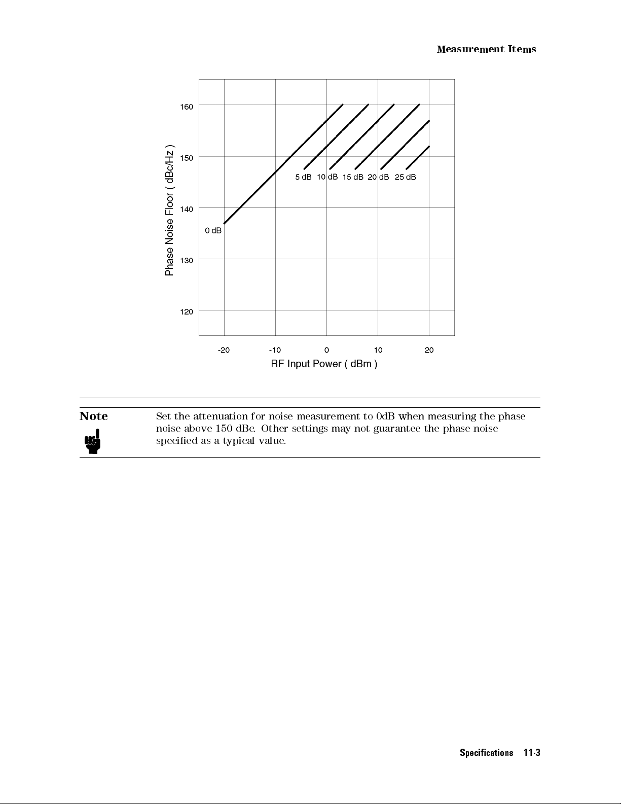
The noise oor at 1 MHz and 9 MHz osets depends on the input signal
level and the RF attenuation setting. The gure shown below illustrates the
relationship between them. The value below each line
setting.
:
:
:
:
::
F
F
F
F
F
FF
FF
FF
F
F
F
F
F
F
auto WIDE
F
not
:
:
:
:
:
:
F
F
F
F
F
be
:
:
:
:
:
:
:
:
:
:
:
:
F
(
CNPLL
assumed
:
in
\General
:
:
:
:
:
:
:
:
:
:
:
:
:
:
:
:
:
:
:
:
:
:
:
:
:
::
:
:
:
:
:
:
:
:
:
:
:
::
WIDE
)
is
selected,
around
the
Characteristics".
::
::
:
:
:
:
:
:
:
:
:
::
:
:
:
:
:
:
:
:
:
::
::
::
:
:
:
:
:
:
:
this
accuracy
measurement point
:
:
:
:
:
:
:
:
:
:
:
:
::
::
:
:
:
:
:
:
6
4dB(typical)
:
:
:
:
:
:
:
:
:
:
:
:
::
::
:
:
:
:
:
:
:
:
:
:
:
:
:
:
:
:
:
:
:
:
:
:
:
:
::
::
::
::
:
:
:
:
:
:
:
:
:
:
:
:
is
valid
at
oset
(for the
tester
show the RF attenuator
:
6
2dB
:
6
4dB
11-2 Specications
Page 4
Measurement
Items
Note
Set
the
attenuation
noise
above
specied as
150
a
typical
dBc
for
.
value
noise
Other
measurement
settings
.
may
to
not
guarantee
0dB
when
measuring
the
phase
the
noise
phase
Specications 11-3
Page 5

Measurement
Items
(Analyzer
Mode)
Measurement Items
RF P
ower Characteristics
Refer to
Frequency/Tuning Sensitivity
Refer to
Phase
Same
Frequency
Frequency
6
The frequency
FSPAN
When
When
When
position
selected
\RF P
\Frequency" in
Noise
as
\C/N
Transient
(frequency
xxxMHz. It
N
N
N
N
N
N
N
N
NN
NN
NN
FREQ
N
N
N
N
N
N
N
N
N
N
N
N
N
N
20MHz
N
N
N
N
N
NN
N
N
N
N
N
N
N
MAX
xxxxMHz
value
inside
ower"
Characteristics
Ratio"
A
NN
SPAN
N
N
N
N
in
ccuracy
span
span is
N
N
N
N
N
N
N
N
N
N
N
N
N
N
N
N
2MHz
N
is
selected:
N
N
N
N
N
N
N
N
N
N
N
N
N
N
NN
,
one
the
in
\Measurement
2
0.1%
is
N
NN
NN
NN
N
N
N
is
of
4352B
(Analyzer Mode)
against DC
\Measurement
\Measurement
+
Time
displayed
selected
NN
N
N
N
is
selected:
20
MHz
selected:
16
measurement
.
The
Control V
Items
(T
ester
Characteristics against
Items
(T
ester
against
below
depending
Depending
frequency
Items
base
the
2
MHz
frequency
Oset
(T
ester
accuracy
frequency
on
the
on
span
oltage
Mode)".
Mode)".
Frequency
Mode)".
of
external
setting
the
entered
bands
of
that
DC
Control
signal
transient
as
(see
measurement
measurement
follows:
target
T
able
V
source
frequency
11-1
)
is
automatically
range
is
oltage
used)
screen,
and
used.
the
as
target
Measurement
The
measurement
When
When
When
the
target
automatically
band
is
Available measurement frequency bands when
Measurement frequency
band number
Maximum frequency
Minimum frequency (MHz) 64 128 192 256 320 384 448 512 576 640 704 768 832 896 960 1024
Frequency span (MHz) 128 256 384 512 640 768 896 1024 1152 1280 1408 1536 1664 1792 1920 2048
Frequency resolution (kHz) 3.2 6.4 9.6 12.8 16 19.2 22.4 25.6 28.8 32 35.2 38.4 41.6 44.8 48 51.2
N
N
N
N
N
N
N
N
N
N
FREQ
N
N
N
NN
NN
NN
NN
20MHz
N
N
NN
N
N
N
N
N
N
MAX
used.
Resolution
N
N
N
N
N
N
N
N
N
N
N
NN
NN
N
N
N
N
SPAN
N
N
N
N
N
N
is selected:
N
N
N
N
N
N
N
N
N
N
N
N
N
NN
NN
NN
xxxxMHz
position
selected
(MHz)
resolution
N
N
N
N
N
N
N
N
N
N
N
2MHz
N
N
N
N
N
N
is
value
1 2 3 4 5 6 7 8 9 10 11 12 13 14 15 16
192 384
depends
N
N
N
N
is
selected:
500 Hz
selected:
,
one
of
inside
the
576 768 960 1152 1354 1536 1728 1920 2112 2304 2496 2688 2880 3000
on
the
50
Hz
Depending
16
measurement
4352B
.
The
Table 11-1.
selected
on
frequency resolution
frequency
the
entered
frequency bands
target
NNNNNN
NNNNNNNNNNNNNNNNNNNNNNNNN
MAX xxxxMHz
span
as
frequency
(see T
of that
NNNN
is selected
follows:
and
able 11-1
measurement
)is
Maximum Sweep Time
11-4 Specications
::::::: :::::: ::::::: ::::::: :::::: ::::::: ::::::: :::::: ::::::: :::::::
20 sec
Page 6

I/O
Signal
Minimum Sweep
Time Base
When the
::
::
::
:
:
:
:
When the
::
::
:
:
:
:
:
:
Spectrum
When
I/O
the detection
Absolute
When
Relative
Ratio
:
:
:
:
:
:
Signal
level
@
0
level
of
:
:
:
0
:
Time Resolution
Accuracy
4352B isn't
:
:
:
:
:
:
:
::
4352B is
:
:
:
:
:
:
:
:
:
mode (
accuracy
5
dBm
is
accuracy
10
dBm
:
:
:
:
:
:
:
:
:
phase locked
::
::
::
::
::
::
phase locked
:
:
::
::
::
::
:
N
NN
NN
NN
NN
N
N
N
N
N
DETECTION
input,
to
::
attenuation=0
0
60
dBm
:
:
:
:
:
:
:
:
:
:
:
:
N
N
N
N
N
N
:
:
:
:
:
:
to
:
:
:
:
:
N
N
N
N
N
N
NN
N
during
:
:
:
:
::
to
:
:
:
the
:
:
)is
:
:
::
::
the
:
:
:
Time
set to
sweep
:
:
:
:
:
:
:
:
:
:
:
:
:
:
:
:
external
::
::
::
::
::
::
external
dB
:
:
::
signal
base
accuracy
the positive
,
@23
6
,
attenuation=0 dB
:
:
:
:
:
:
:
::
::
signal
::
:
10
:
:
:
:
::
::
:
:
:
source
C
:
:
:
:
::
::
source
:
:
:
:
of
peak
:
:
:
:
:
:
:
:
:
:
the
:
:
:
::
:
:
N
(
:
:
:
:
:
:
:
::
::
::
external
NN
NN
NN
NN
N
N
N
N
POS
PEAK
:
:
:
:
:
:
:
6
0.5
:
:
:
:
:
:
::
::
::
signal source
N
N
N
N
N
N
N
N
N
N
N
N
N
).
:
:
::
::
dB
::
::
::
::
:
6
10ppm
::
6
2dBm(typical)
(typical),
12.5
(typical)
used
6
1.5
sec
dB
V
CO
P
ower
V
oltage
Setting
Noise
Setup
Connector
Output
V
CO
Voltage range
Setting accuracy
range
accuracy
@23
6
10
@0
to 40
@10
kHz
time
@Error:
resistance
Control
:::::: ::::::: ::
@23610
Output voltage range
0
15
0Vto
20.0001 V to 35
@0 to 40C
Output voltage range
0
15 V to00.0001 V
0 V to 20 V
20.0001 V to 35 V
Noise
V
oltage
:
:
C
::
::
C
::
::
:
::
::
0.1%
:
:
:
:
:
Voltage
:::::: ::::::
C
Vto
20 V
Output
:
:
:
:
::
:
:
:
:
:
:
:
:
:
:
:
:
:
:
:
:
:
:
:
:
:
:
0
to +15.5
:
:
:
:
:
:
:
:
:
:
:
:
:
:
:
:
:
:
:
:
:
::
::
:
:
:
:
:
:
:
:
:
:
:
:
:
:
:
:
:
:
:
:
:
:
:
:
:
:
:
:
:
:
::
::
:
:
:
:
:
:
:
:
:
:
:
:
:
:
:
:
:
:
:
:
:
:
:
:
:
::
::
::
::
:
:
:
:
:
:
:
:
:
:
:
:
:
:
:
:
:
:
:
:
:
:
:
:
:
::
::
::
:
:
:
:
:
:
:
:
:
:
:
:
:
:
:
:
:
:
:
:
:
:
:
:
::
::
::
::
:
:
:
:
:
:
:
:
:
:
:
:
:
:
(DC)
:
:
:
:
:
:
:
:
:
:
:
:
:
:
:
::
::
::
::
:
:
:
Output
::::::::::::::::::::
::::::: ::
0
0.0001 V
With option 001,
::::::::::::::::::::
:::::::::::::::::::::::
V
::::::: ::::::: :::::: ::::
:::::::::::::::::::::::::::::::::::6f(setting+15 V)20.3%+15 mV
:::::::::::::::::::::::::::::::::::::::::::::::::::::::6(setting20.3%+6 mV)
::::::::::::::::::::::::::::::::::::::6f(setting015 V)20.3%+15 mV
0to20V(20
0
15 to 35 V (20 mA max.), variable in 100-
:::::::::::::::::
:::::::::::::::::::::::::
::::: ::::::: :::
V
(50
mA
max.),
:
:
:
:
:
:
:
:
:
:
:
:
::
::
:
:
:
:
:
:
:
:
:
:
:
:
:
:
:
::
::
:
:
:
:
:
:
:
:
:
::
::
::
::
:
:
:
:
:
:
:
:
:
:
::
::
::
:
:
:
:
:
:
:
:
:
::
::
::
::
:
:
:
:
:
:
:
:
:
:
:
:
:
:
:
:
:
:
:
:
:
:
::
::
::
mA max.), variable in 100-
6f
(setting+15 V)
:::::: :
6f
(setting015 V)
:
:
:
:
variable
:
:
:
:
:
:
:
:
:
:
:
:
:
6
:
:
:
:
:
:
:
:
:
:
:
:
:
6
:
:
:
:
:
:
:
:
:
10nV/
:
:
:
:
:
:
:
:
:
:
<
20
:
:
:
:
:
:
:
:
::
::
::
::
::
:
:
:
:
:
:
:
:
:
:
:
<
2
6
(setting20.1%+2 mV)
2
in
1-mV
(0.2%+2
(0.6%+6
p
H
z
(typical)
msec(typical)
BNC
0.3
(typical)
V
0.1%+5 mV
0.1%+5 mV
steps
mV)
mV)
female
V steps
steps
g
g
g
g
Specications 11-5
Page 7
I/O
Signal
@10
@10
Setup
time
@Error:
Connector
Output
0
to
20
With
kHz
:
::
::
kHz,
voltage
0.1%
:
:
::
::
resistance
V
:
::
::
option
001,
::
:
::
::
::
::
::
::
::
(DC)
:
:
0
:
:
:
:
setting
::
::
::
::
::
:
:
:
:
:
:
15
to 0
:
::
p
H
z
:
<
<
p
:
BNC
10
50
H
(typical)
z
(typical)
female
(typical)
(typical)
:
:
:
:
:
:
::
::
::
::
::
::
::
:
:
:
:
:
:
:
:
:
:
:
::
::
::
::
::
::
::
:
:
:
:
:
:
1nV/
0
15
to
0,
20 to
35 V
(option 001)
::
::
:
:
:
:
:
:
:
:
:
:
:
::
::
::
::
::
::
::
:
:
:
:
:
:
:
:
:
:
:
:
:
::
::
::
::
::
::
::
:
:
:
:
:
:
:
:
:
:
:
:
:
:
:
:
::
::
::
::
:
:
:
:
:
:
:
:
:
:
:
:
:
:
:
,20
to 35
V
:
:
:
:
:
:
:
:
:
:
:
:
:
:
:
:
:
::
::
::
::
:
:
:
:
:
1.5nV/
:
:
:
:
:
:
:
:
:
::
::
::
::
:<
20 msec(typical)
:
:
:
:
::
::
::
::
::
::
::
:
:
:
:
:
:
::
::
::
::
:
:
:
:
:
:
:
:
:
:
:
:
:
::
::
::
:
:
:
:
:
:
:
:
:
:
:
:
:
:
:
Modulation
Frequency
Level
@Open
Setting
Harmonic
Connector
Output
Maximum
RF
Frequency
Input
Connector
Input
@
Open load,
@
Open load,
@1
kHz
Input
level
impedance
@
2 GHz
Accuracy
impedance
Signal
:
:
::
::
::
load
:
::
::
23
0to
Distortion
:
:
:
::
:
:
:
:
:
:
:
:
:
:
:
:
output
range
:
current
:
:
:
:
:
:
:
::
:
:
:
:
:
:
::
:
:
:
:
:
:
Output
::
:
:
:
:
:
:
:
:
C
6
10
40
:
:
:
:
:
:
:
:
:
:
::
::
::
:
:
:
::
::
:
:
:
:
:
:
:
:
:
:
:
:
:
:
:
:
:
:
:
:
:
:
:
:
:
:
:
:
:
:
:
:
:
:
:
:
::
::
::
::
:
:
:
:
:
:
:
:
:
:
:
:
:
:
:
:
:
::
::
::
::
:
:
:
:
:
:
:
:
:
:
:
:
:
:
1
kHz
(xed)
,
:
:
:
:
:
:
:
:
:
:
:
:
:
:
::
::
::
:
:
:
:
:
:
:
:
:
:
:
:
:
:
:
0
to
1
::
::
::
:
:
:
:
:
:
:
:
:
:
:
:
:
:
:
:
:
:
:
::
::
::
:
:
:
:
:
:
:
:
C
::
::
::
:
:
:
:
:
:
:
:
:
:
:
:
:
:
:
:
:
:
:
::
::
::
:
:
:
:
:
:
:
:
:
:
:
:
:
:
:
:
:
:
:
:
:
:
:
:
:
:
::
::
:
:
:
:
:
:
:
:
:
:
:
:
:
:
:
:
:
:
:
:
:
:
:
:
:
:
:
:
:
:
:
:
::
:
:
:
:
:
:
:
:
:
:
:
:
:
:
:
:
:
:
:
:
:
:
:
::
:
:
:
:
:
:
:
:
:
:
:
:
:
:
:
:
:
:
:
::
::
::
:
:
:
:
:
:
:
:
:
:
:
:
:
:
:
:
:
:
:
:
:
:
:
:
::
::
::
::
:
:
:
:
:
:
:
:
:
:
:
:
:
:
:
:
:
::
::
::
:
:
:
:
:
:
:
:
:
:
:
:
:
:
:
:
:
:
:
:
:
::
::
:
:
:
:
:
:
:
:
:
:
:
:
:
:
:
:
:
:
:
:
:
:
:
:
:
:
:
:
:
:
:
:
:
::
:
:
:
:
:
:
:
:
:
:
:
:
:
:
:
:
:
:
:
:
:
:
:
:
:
:
:
:
:
:
:
:
:
:
:
:
:
:
:
:
::
:
:
:
:
:
:
:
:
:
:
:
:
:
:
:
:
:
:
:
:
:
::
:
:
:
:
:
:
:
:
:
:
:
:
:
:
:
:
:
:
:
:
:
:
:
::
:
:
:
:
:
:
:
:
:
:
:
:
:
:
:
:
:
:
:
:
:
:
:
:
:
:
::
:
:
:
:
:
:
:
:
:
:
:
:
:
:
:
:
:
:
:
:
:
:
:
::
:
:
V
rms
:
:
:
:
:
:
:
:
:
:
:
:
:
:
:
::
:
:
:
:
::
:
:
::
:
:
:
:
:
:
variable in
:
:
:
:
:
:
:
:
:
:
:
:
::
::
:
:
:
:
:
:
:
:
:
::
::
:
:
:
:
:
:
:
:
:
:
::
::
:
:
:
:
:
:
:
:
:
:
:
:
:
:
:
:
:
:
:
:
:
:
:
:
::
:
:
:
::
:
:
:
:
:
:
Nominal:
:
:
:
:
:
:
0
10
:
:
:
::
:
:
:
:
:
::
6
(0.5%+1mV
:
6
(1.5%+3mV
:
:
:
<
-40
:
:
:
:
:
:
:
:
:
:
:
5mA
:
:
:
10
dBm
:
:
:
:
:
:
:
:
:
:
50
:
:
:
:
:
:
1mV
dBc(typical)
:
BNC
50
rms
MHz
to
:
:
,
:
:
:
steps
rms
female
(typical)
(typical)
to
3
+20
:
:
N
female
SWR
<
SWR
<
rms
rms
GHz
dBm
1.3
1.2
)
)
11-6 Specications
Page 8

Instrument
B
ASIC
Related Specications
Instrument B
K
eyboard
Connector
I/O
port
Connector
Level
I/O
:
:
:
:
:
:
:
:
:
:
:
:
:
:
:
:
:
:
:
:
:
:
:
ASIC Related
:
:
:
:
::
::
::
::
::
::
::
:
:
:
:
:
::
::
::
::
::
::
::
:
:
:
:
:
::
::
::
::
::
::
::
:
:
:
::
::
::
::
:
:
:
:
:
:
:
:
::
::
::
::
:
:
:
:
:
:
:
:
:
Specications
:
:
:
:
:
:
:
:
:
:
:
::
::
:
:
:
:
:
:
:
:
:
:
:
::
::
:
:
:
:
:
:
:
:
:
:
:
::
::
:
:
:
:
:
:
:
:
:
:
::
::
:
:
:
:
:
:
:
:
::
::
::
::
::
::
::
:
::
::
::
::
::
::
:
:
:
:
:
:
PS/2
style
101
english
::
::
::
::
:
:
:
:
:
:
:
:
:
:
:
::
::
::
::
::
::
::
::
::
::
:
:
:
:
:
:
:
:
:
:
:
::
::
::
::
::
::
:
:
:
:
:
:
:
:
:
:
:
:
:
:
:
:
:
::
::
::
::
:
:
:
:
:
:
:
:
:
:
:
:
:
:
:
:
:
:
:
:
:
::
4-bit input/8-bit
keyboard
::
:
:
:
:
mini-DIN
D-SUB (15-pin)
:
:
:
:
:
:
TTL
level
output port
24-bit
Connector
Level
I/O
I/O
Interface
:
:
:
:
:
:
Figure
:
:
:
::
::
::
::
:
:
:
:
:
::
::
::
:
:
:
:
:
:
:
:
:
::
::
::
:
:
:
:
:
:
:
:
:
:
Figure 11-2. 24-bit I/O Interface Pin Assignment
11-1.
I/O
P
ort
Pin
Assignment
:
:
:
:
:
:
:
:
:
:
:
:
:
:
:
::
::
::
::
:
:
:
:
:
:
:
:
:
:
:
:
:
:
:
:
:
::
::
::
::
:
:
:
:
:
:
:
D-SUB
:
:
:
:
:
:
:
:
:
:
:
::
::
::
:
:
:
:
:
:
:
:
:
:
:
:
:
:
:
:
:
:
:
::
::
::
:
:
:
:
:
:
:
:
:
:
:
:
:
:
:
:
:
:
:
:
:
:
:
::
::
::
:
:
:
:
:
:
:
:
:
:
:
:
:
:
:
:
:
:
:
::
::
::
:
:
:
:
:
8-bit
input/16-bit
(36-pin)
:
:
:
:
:
::
::
:
TTL
output
Specications 11-7
Page 9

General
Characteristics
T
able 11-2.
Signal Source
Assignment
Pin No
.
1 GND 0
2 INPUT1 TTL level,
3 OUTPUT1 TTL
4 OUTPUT2 TTL
5 OUTPUT PORT
6 OUTPUT
7 OUTPUT
8 OUTPUT PORT
9 OUTPUT
10 OUTPUT
11 OUTPUT
12 OUTPUT
13 OUTPUT PORT
14 OUTPUT
15 OUTPUT
16 OUTPUT
17 OUTPUT
18 OUTPUT
19 OUTPUT
20 OUTPUT
21 I/O
22 I/O
23 I/O
24 I/O
25 I/O
26 I/O
27 I/O
28 I/O
29 PORT
30 PORT
31 WRITE STROBE
Signal Name Signal Standard
V
pulse input
level,
latch
level,
latch
TTL level,
TTL
level,
TTL
level,
TTL level,
TTL
level, latch
TTL
level,
TTL
level,
TTL
level,
TTL level,
TTL
level,
TTL
level,
TTL
level,
TTL
level, latch
TTL
level,
TTL
level,
TTL
level,
TTL
level,
TTL
level,
TTL
level,
TTL
level,
TTL
level,
TTL
level,
TTL
level,
TTL
level,
TTL
level,
TTL
level,
TTL level,
latch output
latch
latch
latch
latch
latch
latch
latch output
latch
latch
latch
latch
latch
latch
latch
latch
latch
latch
latch
latch
latch
latch
input
input
active low
PORT
PORT
PORT
PORT
PORT
PORT
PORT
PORT
C
D
PORT
PORT
PORT A4
PORT
PORT
PORT
PORT
PORT
PORT
PORT B4
PORT
PORT
PORT
C0
C1
C2
C3
D0
D1
D2
D3
ST
A
TUS
ST
A
TUS
A0
A1
A2
A3
A5
A6
A7
B0
B1
B2
B3
B5
B6
B7
SIGNAL
typical)
32 +5V PULLUP
33 SWEEP END SIGNAL TTL level, active low
typical)
34 +5V +5V, 100 mA
35 PASS/FAIL SIGNAL
36 PASS/FAIL WRITE STROBE
SIGNAL
TTL level, P
TTL level, active low
typical)
MAX
ASS: HIGH, F
(pulse width:
output
output
output
output
output
output
output
output
output
output
output
output
output
output
output
output
output
output
output
output
output
output
output
output
mode:
mode:
LOW
LOW
,pulse
,
output
,
output
output
, pulse output (width: 20
AIL: LOW
, latch output
, pulse output (width: 10
1
sor
mode:
mode:
(width:
above)
HIGH
HIGH
10
s;
s;
s;
See
4352B GPIB Programming Manual
11-8 Specications
for details.
Page 10

General Characteristics
I/O
Characteristics
General
Characteristics
External
Input
Connector
External
Frequency
Level
Input
Connector
Internal
Frequency
Level
Output
Connector
External
Level
Pulse width
Polarity
Connector
External
Connector
Level
input (
Level
reference input
::
::
Impedance
reference
:
:
impedance
trigger
:
:
program
:
:
1st LO
:
::
::
::
::
::
:
:
:
:
::
::
:
:
:
:
:
:
:
:
:
:
:
:
:
:
:
::
:
:
:
:
:
:
:
:
output
:
:
:
:
:
:
:
:
:
:
:
:
:
:
:
:
:
:
:
:
:
:
:
:
:
:
:
:
input
:
:
:
:
:
:
:
:
:
:
:
:
)
:
(T
::
::
:
:
:
:
:
:
:
::
p
::
:
:
:
:
:
::
::
:
:
:
RUN/CONT
:
:
:
:
:
:
:
:
:
:
:
:
:
:
)
:
:
:
:
:
:
:
:
:
:
:
:
:
:
:
:
:
::
::
::
::
:
:
:
:
:
:
:
:
:
:
:
:
:
:
:
:
:
::
::
::
::
:
:
:
:
:
:
:
+10
dBm(typical)
:
:
:
:
:
:
:
:
:
:
:
:
:
::
::
::
::
:
:
:
:
:
:
:
:
:
:
:
:
:
:
:
:
:
::
::
::
::
:
:
:
:
:
:
:
:
:
:
:
:
:
:
:
:
:
::
:
N
female
:
:
:
:
:
:
:
:
:
:
:
:
:
::
::
::
::
:
:
:
:
:
:
:
:
:
:
:
:
:
:
:
:
:
::
::
::
::
:
:
:
:
10
MHz
6
100
Hz(typical)
:
:
:
:
:
:
:
::
::
::
::
:
:
:
:
:
:
:
:
:
:
:
:
:
:
:
:
:
::
::
::
::
:
:
:
:
:
0
6
dBm
to
+16
dBm(typical)
:
:
:
:
:
:
:
:
:
:
:
:
:
:
:
:
:
::
::
::
::
:
:
:
:
:
:
:
:
:
:
:
:
:
:
:
:
:
::
::
::
::
:
:
:
:
:
:
:
:
:
:
50
(nominal)
:
:
:
:
:
:
:
:
:
::
::
::
::
:
:
:
:
:
:
:
:
:
:
:
:
:
:
:
:
:
::
::
::
::
:
:
:
:
:
:
:
:
:
:
:
:
:
:
:
:
:
::
::
BNC female
:
:
:
:
:
:
:
:
:
:
:
::
::
::
:
:
:
:
:
:
:
:
:
:
:
:
:
:
:
:
:
:
:
::
::
::
:
:
:
:
:
:
:
:
10
MHz
6
100
Hz(typical)
:
:
:
:
:
::
::
::
:
:
:
:
:
:
:
:
:
:
:
:
:
:
:
:
:
:
:
::
::
::
:
:
:
:
:
:
:
:
:
:
:
:
:
:
:
:
:
:
:
::
:
2.5
dBm(typical)
:
:
:
:
:
:
:
:
:
:
:
:
:
:
:
:
:
:
::
::
::
:
:
:
:
:
:
:
:
:
:
:
:
:
:
:
:
:
:
:
::
::
::
:
:
:
:
:
:
:
:
:
:
:
50
(nominal)
:
:
:
:
:
:
:
:
:
:
:
:
:
::
::
:
:
:
:
:
:
:
:
:
:
:
:
:
:
:
:
:
:
:
:
:
::
::
:
:
:
:
:
:
:
:
:
:
:
:
:
:
:
:
:
:
:
:
:
BNC female
:
:
:
:
:
:
:
:
:
::
:
:
:
:
:
:
:
:
:
:
:
:
:
:
:
:
:
:
:
:
:
:
:
::
:
:
:
:
:
:
:
:
:
:
:
:
:
:
:
:
:
:
:
:
:
:
:
::
:
:
:
:
TTL
level
::
:
:
:
:
:
:
:
:
:
:
:
:
:
:
:
:
:
:
:
::
::
::
:
:
:
:
:
:
:
:
:
:
:
:
:
:
:
:
:
:
:
::
::
::
:
:
:
:
:
:
:
2
s
(typical)
:
:
:
:
:
:
:
:
:
:
:
:
::
::
::
::
:
:
:
:
:
:
:
:
:
:
:
:
:
:
:
:
:
::
::
::
::
:
P
ositive/negative
:
:
:
:
:
:
:
:
:
:
:
:
:
:
:
:
:
:
::
::
:
:
:
:
:
:
:
:
:
:
:
:
:
:
:
:
:
:
:
:
:
::
::
:
:
:
:
:
:
:
:
:
:
:
:
input
:
:
:
:
:
:
:
:
:
:
::
::
:
:
:
:
:
:
:
:
:
:
:
:
:
:
:
:
:
:
:
:
:
::
::
:
:
:
:
:
:
:
:
:
:
:
:
:
:
:
:
:
:
:
:
:
:
:
:
:
:
::
:
:
:
:
:
:
:
:
:
:
:
:
:
:
:
:
:
:
:
:
:
:
:
::
:
:
:
:
:
:
:
:
:
:
:
:
:
:
:
:
:
:
:
:
:
:
:
::
:
:
:
:
:
::
:
:
selectable
:
BNC
:
BNC
:
:
:
:
TTL
female
female
level
External monitor output
Connector
Display resolution
LCD
Size/Type
Resolution
::::::::::::::::::::::::::::::::::::::::::::::::::::::::::::::::::
::::: ::::::: :::::: ::::::: ::::::: ::::::: :::::: ::::::: ::::::
:::::::::::::::::::::::::::::::::::::::::::::::::::::::::::::::::
:::::: :::::: ::::::: ::::::: :::::: ::::::: ::::::: :::::: ::::::: ::::::: :::::: :
Figure 11-3. Trigger Signal
D-SUB 15-pin HD
6402480 VGA
8.4 inch color LCD
6402480
Specications 11-9
Page 11

Operation
Conditions
Eective
P
arallel
Interface
Printer
HP
HP DeskJet
HP
HP
HP
HP
DeskJet 1600CM
Operation
Temperature
Disk
Disk
Humidity
@wet
Altitude
W
arm
interface
control
Printer Monochrome
DeskJet
DeskJet
DeskJet
DeskJet
drive
drive
bulb
Disk
drive
Disk
drive
:
up
time
Display
:
:
340J
505
560C
850C
1200
Conditions
non-operating condition
operating
temperature
:
:
:
:
Area
:
:
:
:
:
:
:
:
:
::
::
language
T
able
11-3.
condition
non-operating
operating
:
:
:
:
:
:
:
:
:
:
:
:
::
:
:
:
condition
::
:
:
:
::
::
:
:
:
:
::
::
::
:
:
Supported
p p
p
p p
p p
p p p
p p p
C,
29
condition
:
:
:
:
:
:
:
:
:
:
:
:
:
:
::
::
:
:
:
::
Printing
:
:
:
without
:
:
:
:
:
:
:
:
:
:
:
::
:
:
:
:
:
::
::
::
:
:
:
:
:
::
::
:
:
:
:
:
:
:
:
:
:
:
:
:
:
:
:
:
:
:
:
:
:
:
:
:
:
:
::
::
::
::
:
:
:
:
:
:
:
:
:
::
::
::
::
::
::
::
:
:
:
:
:
:
Printers
Fixed
:
:
:
:
:
:
:
:
condensation
:
:
:
:
:
:
:
:
:
:
:
::
:
:
:
:
and
Color PrintingVariable Color
:
:
:
:
:
:
:
:
:
:
::
:
:
:
:
:
:
:
:
:
:
:
:
:
:
:
:
:
:
::
::
:
:
:
:
:
:
:
::
::
:
:
:
:
:
:
:
::
::
:
:
:
:
Printing
:
:
:
:
:
:
:
:
:
:
:
:
::
:
:
:
:
:
:
:
:
:
:
:
:
:
160
mm
::
:
:
:
Centronics
:
HP PCL3
:
:
::
:
:
:
:
:
:
:
:
:
:
:
:
:
:
:
:
:
:
:
:
:
:
:
:
:
:
:
:
:
:
:
:
:
:
:
2
115
Printer Control
Modes
:
:
:
:
:
:
:
:
:
:
:
:
:
:
:
:
:
::
:
:
:
:
:
:
:
:
:
:
:
:
:
:
:
:
:
:
:
:
:
:
:
:
::
::
:
:
:
:
:
:
:
:
:
::
mm(600
standard
:
:
:
:
:
:
:
:
:
:
:
:
:
:
:
:
:
:
:
::
:
:
:
:
:
0
::
:
:
:
:
:
:
:
:
15%
15%
to
:
:
:
2
compliant
Language
Printing
C
:
:
0
C
10
to
to
2000
:
:
30
430 dots)
to
40
to
40
95% RH
80%
RH
meters
minutes
C
C
Non-operation
Temperature
Humidity
@wet bulb temperature
Altitude
11-10 Specications
::
:::::: :::::: ::::::: :
Conditions
::
::
:
:
:
:
:
:
:
:
:
45
:
:
::
::
::
::
::
::
::
:
:
:
:
:
:
:
C, without condensation
:::::::::::::::::::::::::
:
:
:
:
::
::
::
::
::
::
::
:
:
:
:
:::::: :::
::::: ::::::: :::::: :::::::
:::::: :::::::
:
:
:
:
:
:
:
:
0
20
15% to 95% RH
:
0 to 4572 meters
Cto
60
C
Page 12

Others
EMC
:
Complies
Note:
This
Cet
P
ower
W
eight
Dimensions
:
:
:
:
:
:
:
:
:
::
::
with
Note:
The
4352B
frequency range
however
the
ISM
appareil
,
that
interfering signal.
device complies
ISM est
requirements
:
:
:
:
:
:
:
:
:
:
:
:
:
:
::
::
::
:
Complies
IEC
1000-4-4
meets
between
this
does
conforme
:
:
:
:
::
::
::
:
:
:
:
:
:
:
:
Complies
with
with CISPR
IEC
Complies
(1995)
the specications
27
to
1000
not
apply
with Canadian
ala
:
::
:
:
:
:
:
:
:
90
:
:
:
:
:
:
:
:
:
:
:
:
::
::
::
::
:
:
Complies
Complies
1000-4-2
MHz
when
norme
V
:
:
:
:
:
:
:
:
:
:
with
/
EN
for C/N
when
the
frequency
ICES-001.
NMB-001
to
132
:
:
:
::
::
:
:
:
:
:
:
11
(1990)
with
with
(1995)
IEC
50082-1
ratio and
tested
V
,
or
::
:
:
:
:
:
:
:
::
::
IEC
IEC
/
EN
801-3
(1992)
at
3V/m
to
be
du
198
:
:
:
:
::
::
/
EN
55011
1000-3-2
1000-3-3
50082-1 (1992)
(1984)
/
:
1
kV /
phase noise
in
compliance
measured is
Canada.
V
to
264
:
:
:
:
:
:
:
:
:
:
:
:
:
:
:
:
:
425(W)
Operation
(1991)
(1995)
(1994)
EN
/
/
50082-1
Main,0.5kV /
over
the
entire
with
the same
V
,
47
to
:
::
::
::
:
2
235(H)
Conditions
:
Group
EN
6100-3-2 (1995)
EN
6100-3-3 (1995)
:4
kV CD
(1992)
immunity
IEC
801-3/1984.
as the
test frequency
63
Hz, 300
:
:
:
:
:
:
:
:
21.5
2
1,
Class
,8
kV AD
:
3
V/m
Signal Line
test
Note
V
A
max
kg
max
553(D)
mm
A
,
of
Specications 11-11
 Loading...