

Page 1

LIST
OF
SECTION
SECTION
TABLE
OF CONTENTS
ILLUSTRATIONS
ONE--INTRODUCTION
Main
Conponents
Case
design
Differences
from
520l1040ST
TWO..THEORY
OF OPERATION
Overview
Main
Systen
Microprocessing
unit
GIue
Main
Menory
Direct
l4enory
Access
MFP Interrupt
Control
Audio/Video
subsystem
Video
Shifter
Video Display
Menory
GIue
Memory Control-Ler
Sound
Synthesizer
Video Interface
Input/output
subsystens
MIDI
Intelligent
Keyboard
Parallel Interface
RS232
Interface
Disk Drive
Interface
Hard
Disk
Interface
Systen Startup
System Errors
Functional
block
diagran
Systen
clock
diagra-m
t.2
t.2
I.5
2.t
2.2
2.2
2.2
2.3
2.3
2.4
2.5
2.5
2.5
2.6
2.6
2.6
2.6
2.8
2.8
2.9
2.70
2.Lt
2.L2
2.L3
2.t4
2.15
2.L6
2.t7
11
Mega
Service
Manua1
i.1
Table
of Contents
Page 2

SECTION
THREE--TESTING
THE
MBGA
Overview
Test equipnent
Test Configuration
Trouble-Shooting
a
dead
unit
ST
Diagnostic
Cartridge
Power-up
RAM test
ROM
test
Color test
Keyboard
test
MIDI test
RS232 test
Audio test
Tining test
DMA test
Floppy
Disk test
Printer/Joystick
test
High
Res
Monitor
Blitter test
Clock
test
Expansion
port
test
Error
Codes
Quick
Reference
SECTION
FOUR--DISASSBMBLY/ASSEMBLY
SECTION
FIVE-.SYMPTOM
CHECKLIST
Display
problems
Disk
Drive
Problens
Keyboard
problens
MIDI
problems
R5232
problens
Printer
Problems
Hard
Disk
Problens
Real
Time
Clock
Problens
Blitter
Problens
3.1
3.1
3.2
3.2
3.4
3.4
3.6
3.7
3.7
3.9
3.9
3.
10
3.
11
3.r7
3.r2
3.
13
3.t5
3.16
3.L6
3.L7
3.r7
3.18
5.t
5.L
5.2
5.2
5.2
5.2
5.2
5.2
5.2
í.2
Mega Service
Manual
Table of
Contents
Page 3

SECTION
SIX.-DIAGNOSTIC
FLOIlICHARTS
SECTION
SEVEN..PARTS
LIST AND
ASSEMBLY
DRAWINGS
SECTION
EIGHT-.SCHEMATICS
AND
SILKSCREEI'I
SECTION
NINE--GLOSSARY
Mega
Service
Manual
i.3
Tab1e of
Contents
Page 4

LIST OF
ILLUSTRATIONS
FIG 1
MEGA
COMPUTER
FIG
2 BATTERY COMPARTMEI.IT
FIG
3
BACK PANEL
FIG 4
I,EM
SIDE
PANEL
FIG
5
TOP
OF
KEYBOARD
FIG
6
BOTTOM OF
KEYBOARD
FIG
7
MEGA MOUSE
FrG
I
t{oNrron
poRr
FIG
9
MIDI PORTS
FrG
10 MoUSE/JOY
PoRTS
FIG
11 PRINTER
PORT
FrG 12
RS232 PoRT
FIG 13
EXTERNAL
FLOPPY
PORT
FIG 14 EXTERNAL
HARD DISK
PORT
FrG 15
FLJNCTTONAL
BLoCK
DTAGRAM
FIG
16
SYSTEM
CLOCKS
1.1
L.2
1.3
r.3
1.4
1.4
1.5
2.7
2.8
2.9
2.LO
2.tL
2.L2
2.L3
2.16
2.r7
Mega Service
Manual
11 List
of
Illustrations
Page 5

SECTION ONE
INTRODUCTION
The Mega
2
and
Mega
4 are Motorola
MC68000 nicroprocessor based
conputers with
sinilar
architectures
to the
520ST/
1040ST line. They
are
styled as
a
nain CPU
unit
with a detached
keyboard. The Mega 2 has
2 negabytes
of RAM,
the Mega 4 contains 4 negabytes. Both the Viega
2
and
Mega
4 have
a built-in 1 Megabyte
(720K
fornatted)
3,5
inch floppy
disk
drive,
and an internal switching
power
supply with built-in
cooling fan.
Since the
onty difference between
the
Mega 2
and
Mega
4 is the
size
of its RAM,
this
nar¡ual
will
use
'
Mega
'
as a
generic
tern
which
refers
to both
products.
Power Light
Disk
Drive
Drive Busy Light
FIG. 1
COMPUTER SYSTEM
Mega
Service
Manua1
ItIEGA
1.1
Introduction
Page 6

The main
components
of
the
Mega 2 and
Mega
4 are:
CPU
Main board assembly
Disk drive
Power supply
& cooling
fan
RF Shield
(upper
and
lower)
CPU
Plastic case
(upper
and
lower)
KEYBOARD
Keyboard assembly
Interface board
assembly
Keyboard
Plastics
(upper
and
lower)
MOUSE
Mouse board assembly
Mouse Plastics
(upper
and
lower)
CASE
DESIGN
shows
the
CPU
portion
and figure
7
shows the
o
o
o
o
o
o
o
o
o
o
Figures
1
thru 4
keyboard
portion,
Battery
Housing
of the
IUEGA,
5
ar¡d
6
mouse.
shows
the
Cover
--
size AA Batteries
+
Top
of
Computer
(+)(-)
FIG. 2
BATTERY COMPARTMENT
Mega
Service
Manual
r.2
Introduction
Page 7

On/Off
lo
Power
Js
Frc.
3
BACK PANEL
FIG. 4
LEFT SIDE PANEL
loppy
I
Printer
Midi
ln
Cartridge
Keyboard
Mega
Service
Manual 1.3
Introduction
Page 8

Function
Keys
I
¡oyst¡Jx
Port
I
FIG.
5
TOP OF KEYBOARD
Arrow
Keys
Bottom
of
Keyboard
Calculator
Keypad
Computer
Jack
V
I
MouseiJoystick
FIG.
5
BOTTOM OF KEYBOARD
Mega
Service
Manual
1
.ll
Introduction
Page 9

Clicking
Left Mouse
Button
Right
Mouse
Button
FrG.
7
MEGA
UOUSE
Differences
fron
520ST/1040ST
o
New version of
T0S
o More
nenory requiring
74LS243
buffers on
MAD lines
o
ReaI
tine
clock chip
& support circuit,
o
Graphics Co-Processor
(BITtsLiT)
o
Internal expansion
connector
& support circuit
o
Cooling
fan
o
New
case
styling with
detached
keyboard
Mega
Service
Manual
r.5 Introducti.on
Page 10

Page 11

SECTION
T!{O
THEORY OF OPERATION
OVERVIEW
The Mega 2 and
Mega 4 share a coruDon architecture,
using the sa.ne
LSI
chip set,
and case styling.
Ttre only difference
is the addition
of
one
ba¡rk of
2 Mega-bytes of
RAM, for a total of 4
Mega-bytes of
RAM
on
the Mega 4.
Ttre hardware can be considered
as consisting of
a
nain
systen
(central processing
unit ar¡d
support chips)
a¡rd several
Input/Output subsystens
.
Main
System
o
Mc680o0 running at SMltz
o
192 Kbyte Read Only
Memory
o
2
or 4
Mega-byte
Randon Access Menory
o
Direct Menory
Access
support
o Systen
tining and
Bus control
o
Interrupt control
Audio/Video Subsystem
o
Bit Mapped video display,
using
l2k
bytes of
RAM, relocatable
anywhere
in nenory.
There
are
three display
nodes available:
a.
32O
x 200
pixel,
16
color
palette
îron
jL2
selectÍons
b. 640
x 200
pixel,
4
color
palette
fron
!12
selections
c. 640
x
400
pixet,
nonochrone
o
BITBLiT
support
o
Monitor
interface analog:
RGB, Monochrone
o
Audio output:
programmable
sound chip
with
J
voices
Input/Output Subsystens
o
Intelligent
Keyboard
with
2
button
mouse/ioystick interface
o
Parallel
printer
interface
(Centronics)
o
RS-232C serial
interface
o
DMA
Port & connector
for
external
drive
o
Hard disk
drive
interface &
Laser
Printer
o
Musical
instrunent
network connunication
:
Musical
Instrunent
Digital
Interface
(MIDI).
o
ReaI
Time Clock with
battery
backup
o
ROM
Port
Mega
Service
ManuaL
2.7
Theory of Operation
Page 12

MAIN
SYSTEM
The
main system
includes
the
microprocessing
unit,
main
nemory
(ROM
and
RAM)
,
systen
control,
intepupt
control,
and
general
purpose
DMA controller.
MicroProcessing
Unit
The
Mega uses
the
Motorola
MC68000
16 bit
external/32
bj-t
internal
data
bus,
Z4 Uit
address
bus
nicroprocessor,
running
at
I
Mflz.
Glue
Glue
(naned
because
it holds
the
systen
together)
is
such an
important
component
that
it
is
involved
in nearly
every
operation
in
thè
computer.
The
functions
nay be
sumnarÍzed
as
follows:
Clock
dividers--
takes
ttre
I
Mtlz clock
and outputs
2
Mllz and
500
KHz clocks.
Video
tining--
B-Lank,
DE
(Display
Enable),
Jlsync:
gnd Hsync
are
use¿
to
generãtlsignals
for
the
video
display.
There
is a
Ìead/Write
register
in Gtue
wfrich
nay be
written
to
configUre
for
50
or
60 Hz
operation
(done
by
the
Operating
System).
Interrupt
priority--
interrupts
fron the
MFP
and video
tining
are
codeffisofpriorityonoutputsIP11andÍPL2tothe
68000.
These
leve1s
correspond
to
no
interrupts,
MFP
interrupts,
VSYNC
interrupt,
HSYNC
interruPt.
Signa]
and
Bus
qlbitration--
Glue
decodes
addresses
to
generate
crrip
,
DMA
Controller,
Progranmable
Sound
Genàrator,
Memory
Controller,
and
ROMs.
It
receives
signals
from the
MFP,
DMA,
Menory
Controller,
to
synchronize
data
transfer.
It arbitrates
the
bus
during
DMA transfers
to
prevent
CPU and
DMA
devices
from
interfering
with
each
other
(see
DMA
below)
'
IlleEal
condition
detectiq4--Glue
asserts
Bus
Error
(BERR)
if
writing
to
ROM,
writing
byte
writing
to
system
DeII¡ory
when
the
processor
is
in user
mode.
AIso occurs
if a
device
does
not
respond within
the
required tine
linit.
For example,
the
CPU
tries to
read
from
nemory
and
the
Memory
Controller
does
not
assert
DTACK.
certain
conditions
are
violated,
such
as
sized
data
to
a word sized
register,
or
Mega Service
Ma¡rual
2.2
Theory
of
Operation
Page 13

Main
Menory
Main
menory
consists
of L92 kbytes
of ROM
and
one
or
two
banks
(2
Mega-byte
each) of d¡manic RAM.
rn
addition,
the
cartridge
sLot alrows
access
to 128 Kbytes
of
ROM.
All
nenory is
directly
addressable.
The
components
of
the
ne¡nory
systen
are:
ROM,
RAM,
RAM
buffers, Menory
controller,
a¡¡d
Glue. Tt¡e
Operating
System resides
nostly
in
ROM,
wíth
optional
segnents loaded
fron
disk into RAM.
R.{M is
organized
as
16
bit
words
and
nay
be
accessed 16
bits
at a
tine
or
8 bits
at a tine.
Even nunbered
addresses refer
to the high
I
bits
of a word
and odd addresses
refer
to the low
I bits. RAIII
ís made
up
of
1 Megabit
X 1
chips; in
the Mega 2
there
are 16
chips,
giving
z
Mbytes,
while in
the Mega
4 there is
a¡r additional
bank
of L6
chips,
giving
two tines
the
nemory,
or 4 Mbytes.
BAM menory
nap:
000008-000800
Systen nenory
(priveliged
access)
000800-1FFFFF
low
bank
200000-3FFFFF
high
bank
(Mega
4 only)
Note:
the
first
8 bytes
of ROM are napped
into
addresses
O-7.
These
are reset
vectors
which the
68000 uses
on start-up.
The
Operating
Systen is located
in
two
lMeg
x
I
ROM
chips
in
current
versions
(192k).
Menory
Controller--takes
addresses fron
the address
bus and
converts
to Row Address
Strobe
(RAS)
and Column
Address
Strobe
(CAS).
All
RAIì|
accesses
are controlled
by this Atari
proprietary
chip,
which
is
progrannable
for
up to 4
Megabytes
of
nenory.
Tt¡e
Operating
System
determines how
nuch Eernory
is
present
and
prograns
the
Menory
Controller
at
poner-up.
Ttre Memory
Controller refreshes
the
dynanic
RAMs,
loads
the Video Shifter
with display
data,
and
gives
or
receives
data
during direct nernory
access
(DMA).
Glue--decodes
addresses for RAM
a¡rd ROM
a¡rd asserts
output
signals
to
enable these devices
(also
decodes
addresses for
nost
hardware
registers
to
provide
chip selects,
as well as nany
other
functions.
See Glue
description
above.
).
Direct Menory Access
Direct
menory
access is
provided
to
support both low
speed
(25O
to
500
Kilobits/sec)
and
high
speed
(up
to 8
Megabits/sec)
Sbit device
controllers.
The floppy
disks transfer
data via low
speed
DMA
and the
hard
disk
(or
other devices on the hard
disk
port)
transfer
at high
speed.
For DlvlA
to take
place,
the
Menory
Controller
is
given
the
address
of
where to tal<e data
fron
or
put
data
in
RAM,
the
DMA
Controller
is
set up
(which
channel,
high
speed or low
speed, and how
many
bytes)
and the
peripheral
is
given
a
comnand to send
or
receive
data. The
entire block of data
(the
size
must
be
given
to
the
DMA
Controller
and
the
peripheral
before the
operation
starts)
is
then
transferred
to or
from menory
without intervention
by the CPU.
Mega
Service Manual
2.3
Theory
of Operation
Page 14

For
exanple,
in a
transfer
of
a
sector
fron
the
floppy
to
nenory'
the
floppy
conúro1ler
will
signal
the
DItlA,
Controller
that
a
byte
is
ready
by
asserti"á
ponO,
tn"
óue chip
will
read
the
byte
ar¡d
signal
Ci".l
Glüe
will
signal
the
Menory
Controller,
-and
the
Menory
Controller
will
read
the
byte
fron
the
DMA
Óontrotler
a¡rd
place
it
in
the
address
which
was
set
up
previously.
The
DMA
Controller
will
then
wait
for the
next
byte
fron
thè
floppy
controller,
and
the
process
wítl
repeat
until
Itr"
äpecified
number
ôr
uyt"s
has
been
transferred'
Tra¡rsfers
from
nenory
to
fJ-oppy
are
sinilár.
The
floppy
initiates
every
transfer
by
requesting
data
on
FDRQ.
At
high
speed
(hard
disk
port),
there
is
a
difference:
as
a
byte
is
ready
to
transfer
to
or
fron
the
DMA chip,
the
DMA
Controller
will
assert
ACK
to
tel
tne
peripheral
know
the
byte
ís
avaÍlable
or
has been
reaa.
The
DMA
Controller
can
store
up
to
l2
bytes
in
internal
De¡rory'
This
is
,r."."".ry
if the
68000
is using
the
bus,
and
the
DMA
nust
wait
to
transfer
to
ä.roty.
Data
nay
be
input
fron
the
port
without
being
lost
or
slowing
down
the
tra¡¡sfer
speed'
MFP
InterruPt
Control
The
68901
MFP
handles
up
to
16
interrupts.
Currently
all
but
one
are
used.
Each
interrupt
can
be
nasked
off
or
disabled
by
progrernning
ñ;
MFp.
Th;8
inputs
äre
also
directly
readable
by
the
CPU.
When
the
MFp
receives
an
inlerrupt
input,
or
generates
an
interrupt
internally,
if the
interrupt
is enatled,-MFPlyf
witt
be
driven
low.
When
the
CPU
is
ready
to
respond,
it
signals
interrupt
acknowledge
(Fco-2ìigh and
vltlA
Iow)
and
GIue
*nilI
."""tt
r¡cr
(interrupt
acknowledge).
The
MFP
will
assert
DTACK
and
put
a
vector
number
on
the
data
bus,
which
the
cPU
will
read
and
use
lo
calculate
the
address
of
the
interrupt
routine'
The
interrupts
controlted
by
the
MFP
are:
nonochrone
monitor
derecr
(MONOMOÑI-,--R5232
(including
CTS,
999,
RI),
disk
(FDINT
a¡rd
HDINT),
parallef'óort
gÚSV,
display
enable
(DE,
equals
start
of
display
iine),'S'giO
IRQs
ior
keyboard
and
MIDI
data,
and
MFP timers.
ñoi árr
l/O
operations
use
interrupts.
The
CPU can
also
poll
the
MFp
while
waitini
for
an
operation
to
conplete.
The
MFP
has
four
timers,
used
by
tñe
Operating
System
for
event
tining
and
used
by
the
RS232
port
for
transnit
and
receive
clocks'
Mega
Service
ltlanual
2.4
Theory
of
OPeration
Page 15

AUDIO/VIDEO
SUBSYSTEM
The
video
subsysten
consists
of
the video display nenory,
the
Menory
controller,
Glue,
a
graphics
control chip
(video
shifter),
a
graphics
processing
unit
(BImLiT)
,
and a discrete
section
to drive
the
video
output.
The audio
subsysten
consists
of
a
Progra.mnable
Sound
Generator
chip with a transistor
output
anplifier.
Video
Shifter
There
are 16
color
palette
registers
Ín
the shifter.
AII 16
are
nay
be used in
row resorution,
4
nay
be used
in
high
resolution,
a¡¡d
only
one
is
used in high resorution
(actuarly,
onry bit
0
of
register
0
is
used
for inverse/nornal
video). Each
palette
is
progr¡mmed
for
8
Ievels
of intensity
of red,
blue,
and
green,
so
there
are 8 x
I x I
=
112
colors
possible.
For
a
given
pixel,
the coror
which is
displayed
is
taken fron
the
palette
referred
to by
getting
infornation
from
each
logical
plane (see
description
of
video
dispray menory
betow). The
shifter
will
output the red,
green,
and
blue
levers
specified
by
that
palette;
note
there are three
outputs for
each color. Each
output is
either
on or off. Thus,
the nu¡nber
of
possible
output levels
is
Z to
the
lrd
power
=
$. The
three
outputs
are sr¡nmed
through
a resistor
network
to
proportion
the voltage level
to
give
I equal
steps. In
monochrome
node,
the
color
palettes
are bypassed
a¡rd there is
a
separate
output.
Video Display
Menory
Display
nemory
is
part
of nain nenory
with
the
physical
screen
origin
located
at the top left
corner
of the
screen.
Display
Eenory
is
configured as 1, 2,
or
4
(nigh,
nediun,
or
1ow
resolution)
Iogical
planes
interwoven
by 16 bit
words into
contiguous
nemory
to forn
one
32
Kilobyte
physical
plane
starting
at a 256 byte
half
page
boundary. The
starting address of display
Eer¡ory is
placed
in
the Menory
Controller's
Video
Base
Address
register
by
the Operating
Systen
or
application. The Menory
Controller
will load
display
infornation
into
the video
Shifter 16
uits
at a tine,
and the Video
Shifter
wirl
decode this infornation
to
generate
a seriar
dispray
strean. rn
nonochrone
mode,
each bit represents
1
pixer
on or off. rn
color,
bits
are conbined fron
each
plane
to
generate
the comect level
of red,
green,
and blue.
For
exanple, in
low resolution
(4
ptanes)
4 words
are
loaded
into
the
Video Shifter for
each
word
(16
pixels
displayed
on the
screen. Tt¡e
Video
Shifter
conbines
bit 0 from
each word
to forn
a four
bit
nunber
(0-15),
and takes the
color
from
the
palette
referenced
by that
nunber
(e.s.
0101=5,
use color from
palette
register
!)
a¡rd
outputs
those revers,
then takes
bit
1 fron
each
plane
and outputs
the coror
from
the
palette
referenced
by those four
bits,
etc.
Mega
Service ManuaÌ 2.5
Theory
of Operation
Page 16

G1ue
GIue
provides
tining
control
to
the
Menory
Controller,
video
output,
and
monitor/RF output.
VSYNC
input
to
the
Menory
Controller
causes
the
starting
address
of
the
display
nenory
to be
reloaded
into
the
address
counter
during
vertical
blanking.
DISPLAY
EI{ABLE
(DE)
tells
the
Memory
Controller
a¡¡d
Video
ShÍfter
that
a display
line
ís being
scanned
anâ
data
shoutd
be
loaded
into
the
Vídeo
Shifter.
BLANK shuts
off
the
video
output
fron the
Video
Shifter
during
periods
when
the
scan
is
not
in a
dilplayable
part
of
the
screen.
VSYNC
and
HSYNC
both
go
to
the
monitor
output
a¡rd
RF
modulator.
These
signals
synchronize
the
nonitor
or
T.V.
vertical
a¡rd
horizontal
sweep
to
the
display
sigPal.
Menory
Controller
In addition
to
the
inputs
from
Glue
nentioned
above,
there
are two
output
control
signals
associated
with
video.
DCYC
strobes
data
from
display
nenory
lñto tne
Video
Shifter.
CMPCS
(color
nap select)
is
active-only
when
changing
the color
attributes
in
the
color
palettes.
Sound
SYnthesizer
The
yM2149
Progranmable
Sound
Generator
(PSG)
produces
nusic
synthesis,
sound
effects,
and audio
feedback
(e.g.
alarns
a¡rd
key
"ii"t
"¡.
The clock
input
ís
2 MHz; the
frequency
response
range
is
30
Hz to
tZJ
KHz,
There are
three
sound
channels
output
fron
the
chip,
which
are
míxed and
sent
to the
nonitor
speaker.
The
pSG
is also
used
in
the
system
for
various
f/O
functions
relating to
printer
port,
disk
drive,
and
RS232.
This
Iocation
r.s
to
Atari
Blitter
a
DMA device
that
moves
block
of
nenory
data
fron a source
a destination
location
through
a
given
logic
operation.
Single
or
multiple
word
increments
and
decrenents
are
provided
for
transfer
to destination.
There are
16
possible logic operation
rules
associated
with
the
merging
of
source
a¡rd
destination
data.
In
addition,
with
the
16 wõrd
patterns ran a¡rd
three
L6 bit
end-nask
registers,
the
blit can
also
be
used to
perforn
operations
such
as area
seãd
filling,
pattern
filling,
brush
line
drawing,
text
and
graphic
transformations,
etc.
For
more infornation,
please
refer
to
the
user
nanual
which
is
included
in the
Developer
Kit.
Mega
Service
Manual
2.6
Theory of
Operation
Page 17

Real
Tine
Clock
with
Battery Backup
Ttris
device has
counters for
Time
and Calendar
buÍIt-in. Clock
data
are expressed with BCD
code. The
lower four
address
and data
Iines
are
used to
program
the device
and access
the clock
through
signal lines
RTCCS, RTCRD, RTCh¡R
which
generated
fron
a decoder. A
RESET
line is
also
provided
to reset
the chip when
the system is reset.
The
naín clock supplied to
the devÍce is
a
32.768
l<hz
oscillator
which
will
be adjusted by a trimmer condenser
so that it
will output
through
the CLKOIJII
line
a standard
clock signal
of
16.384 Xfrz.
In
addition, a
JV
battery backup ca¡¡ be used
to
keep
the clock running
during
power
down.
For nore
detail,
please
refer
to
the application na¡rual
fron
the
nanufacturer
(RICOH
part
number RP5C15)
Mega
Service Manual 2.7
Theory
of Operation
Page 18

Video
Interface
The
th¡o
types
of
interface
are
provided in the
Megas
are
a¡alog
RGB a¡rd
nonochrone.
The
presence
of
a
nonochrone
nonitor
ís detected
by
the
MONOMQN
input
(when
â
nonochrone
nonitor
is connected,
it
will
be
Iow).
The
possible
disPlays
are:
Monochrome:
single
enitter
foltower
a.nplifier
driving
the output
of
the
Video
Shifter.
RGB:
resistor
network
sums
colors
each
have an
output.
Monitor
Inputs:
outputs
for each
color.
Ttre
three
emitter
follower
a.mplifier
to
drive
Hsync--TTL
level,
negative,
3.3
k ohn.
Vsync--TIL
Ievel,
negative,
3.3
k ohn.
Monochrone--digital
1.0V
P-P'
J!
ohn.
R,G,B--analog
0-1.OV
P-P'
75
ohn.
Audio--1V.
P-P,
1k ohn.
û
Monitor
1
-
Audio
Out
2
-
ComPosite
SYnc
3
-
General
PurPose
OutPut
4
-
Monochrome
Detedt
5
-
Audio
ln
6
-
Green
7-Red
I
-
Plus
12-Voll
Pullup
9
-
Horizontal
SYnc
FIG.
8
MONITOR
PORT
10 - Blue
11
-
Monochrome
12
-
Vertical
Sync
13
-
Ground
Mega Service
Manual
2.8
Theory
of
Operation
Page 19

rNPUT/oUTPUT
SUBSYSTEMS
Musical
Instrument
Connunication
The
Musical
Instrunent
Digital
Interface
(MIDI)
allows
the
integration
of
the
Mega
with
nusiõ
sysnthesizers'
sequencers'
drun boxes
and
other
devices
fossessing
MIDI
interfaces.
HiSh
speed
(3L'25
Kilobaud)
as¡rnchronous
current
loop
serial
communication
of
keyboard
"rrd
ptog"an ilfornation
is
provided
by
two
ports, MIDI
gUT
and
MIDI
IN
(MIDI
oUT
also
supports
the
optionat
ttlt¡t
ntnu
port)
.
MIDI
specifies
thar
data
co.rsi"f'ãi
8
A.t.
bits
preceded by
one
start
bit
a¡rd
followed
by
one
stoP
bit.
Connunication
takes
place
via
a
6850
nCfe.
The
CPU
reads
and
writeJ-to
l[ã-OóiO
in
response
to
interrupts
which
are
passed
fron
the
6850
to
the
MFP
interrupt
controller.
Ttre
systen
is
interfaced
to the
outside
via
trdo
inverters
on
the
tra¡rsnit
side
a¡rd
an
LED/photo-
transistor
chip
on
the
input
side.
The
input
signal
is routed
around
through
two
inverters
to
the
output
connector
where
it
is called
II{IDI
THRU
in
order
to
allow
chaining
of
nultiple
devices
on the
MIDI
bus'
Js
J¡
Midi
Out
1
-
THRU
Transmit
Data
2
-
Shield
Ground
3
-
THRU
LooP
Return
4
-
OUT
Transmit
Data
5
-
OUT
LooP
Return
Midi
ln
1
-
Not
Connected
2
-
Not
Connected
3
-
Not Connected
4
-
lN
Receive
Data
5
-
lN
LooP
Return
FIG.
9
MIDI
PORTS
Mega
Service
Manual
2.9
Theory
of
OPer'ttion
Page 20

Intelligent Keyboard
The
keyboard
trarismits
nake/break
key scan codes,
ASCII
codes,
nouse data,
joystick
data,
in response
to external
events, and
tine-
of-day data
(year,
month, day,
hour, minute,
second)
in response
to
requests by the
CPU. Comnunication is
controlled
on the
nain
board by
a
6850 device
a¡rd
on
the keyboard assenbly by the
lMHz
8 bit
HD6301
Microconputer Unit.
The HD6301 has internal RAM
and
RoM. Included in
ROM are self-test diagnostics which are
perforned
at
poh'er-up
and
whenever the
RESET
connand
is
sent over
the serial connunication
line
by the CPU.
The MC6850 is read
a¡¡d written to
by the CPU in response to
interrupts
which are
passed
to
the
CPU by Èhe
MFP interrupt
controller.
The 2 Button Mouse is
a¡r opto-mechanical
device with the
following
characteristics: a resolution of
100
counts/inch,
a
mæ<imun
velocity of
10 inches/second
and a
naxinum
pulse phase
error of
50
percent.
The
joystick/nouse
port
has inputs
for
up, down,
left, ríght, right
button,
Ieft
button.
The right
button
equals the
joystick
trigger, a.nd the
left
button
is
wired to the second
joystick
port
trigger.
The
joystick
has
four
directions
(up,
down, etc. ) and
one trigger.
Mouse/Joystick
1
-
Up/XB
2
-
Down/XA
3 - Left/YA
4 - Right/YB
5
-
Not
Connected
6
-
Fire/Left
Bulton
7-
+sVDC
I
-
Ground
9
-
Joyl
Fire/Right
Bulton
1-up
2
-
Down
3 - Lefl
4
-
Right
5
-
Reserved
6
-
Fire
Button
7-
+SVDC
8
-
Ground
9
-
Not
Connected
FIG.
10
MOusE/JoY
PoRT
v
Joystick
3
Mega
Service Manual
2.ro
Theory
of
Operation
Page 21

Parallel
Interface
The
parallel
port
is
prinarily
intended
as
a Centronics
type
printer
interface,
but
can also
be used as a
general
purpose
r/0
port.
centronics
STROBE
and
BUSY
are
supported. BUSY
is read
by the MFp
chip.
Data
and strobe
signals
are output
by the YM2149
psc
chíp.
Not
all
Centronics
printers
are compatible
with
this
port.
The
current
loading
on
the data lines
should
not
exceed 2.3 mA.
(TtrÍs
corresponds
to
a
2.2k
ohn resistor
pull-up
on the
printer
side.
)
Ttre
port
can
be
programned
to
be
read
directly
by the CPU,
with
Gtue
chip
select.
input
or output.
The
PSG
chip
is
doing
address
decode
to
provide
ç
Printer
1
-
STROBE
Output
2-Dala0
3-Data1
4-Dala2
5-Data3
6-Data4
7-Data5
8-Dala6
9-Dala7
aaaaaaaaaaaaa
aaaaaaaaaaaa
?5 .r¡
2l :2 l!
2f
19
16
rr 16
!5
10
-
Not
Connected
11
-
BUSY
lnput
12-17
-
Not
Connected
18-25
-
Ground
FIG. 11
PRINTER PORT
Mega
Service Manual
2.17
Theory
of Operation
Page 22

RS232C Interface
The
RS232C
interface
provides
asynchronous
serial
connt¡¡¡ication
with
five
handshake control
signals:
Reguest to
Send
a¡rd
Data
Terninal
Ready are
output
by the
PSG chip;
Clear to
Send,
Data
Carrier
Detect,
and
Ring
Detect are
input to the
MFP
chip.
The
MFP
contains
a
USART
(Universal
Synchronous/Asynchronous
Receiver/Tra¡rsnitter)
which
handles
data
transmission
and
reception.
The
2.4576
MHz clock
to
the
MFP
is
divided by the
tiner
D
(pin
16) output
of
the
MFP
to
provide
the
basic
clock
for receiver
and
transnitter.
Data
rate of
50
to
19200
bits
per
second
are
supported.
f488 tine drivers
and
1489
line receivers
with
+/-
I2v. supply
meet the
EIA
RS232C
standard
for electrical
interface.
\
Modem
1
-
Protective
Ground
2
-
Transmitted
Data
3
-
Received Data
4
-
Requesl
to
Send
5 - Clear
lo Send
6
-
Not Connected
7 - Signal
Ground
8
-
Data
Carrier
RePeat
9-19
-
Not Connected
'¡
aaaaaaaaaaaaa
aaaaaaaaaaaa
2t
20
-
Data
Terminal Ready
21
-
Not Connected
22
-
Ring lndicator
23-25
-
Not
Connected
FIG.
T2
RS232
PoRT
Mega Service
Manuaf
2.L2
Theory of
Operation
Page 23

Disk Drive
Interface
The Mega
conputers
have
a
built-in floppy
disk controller
(a
lrJestern
Digital
L772) and
logic for
selecting
up to
trr¡o single
or
double sided drives. The Mega has one built-in
floppy disk
drive a¡rd
provision
for
one external disk drive. The hlestern Digital WDt772
Controller
services both drives. Drive
and side selection
is
done
by
outputs
on the
YM2149 PSG
chip. The CPU reads
a¡rd writes
to the
L772
through
the
DMA
Controller,
Tl:e 1772
Ínterrupts
the CPU on
the
INTR
Iine, via
the
MFP interrupt
controller. Tl:re L772
accepts
high
level
comnands, such as
seek,
fornat
track,
write
sector,
read
sector,
etc.
and
passes
data to the
DMA Controller
(see
DMA
controller under
Main
Systen,
above,
for
details
on DMA
tra¡rsfer).
The L772 ínbemupts the
CPU
when the operation
is
conplete.
The
CPU
is
freed fron
nuch
of the
overhead of disk I/0.
I
Floppy
tlsk
1 - Read Dala
2-Side0Select
3
-
Logic Ground
4 - lndex
Pulse
5-Drive0Select
6-DrivelSelect
7 - Logic
Ground
I
-
Motor
On
9 - Direction
ln
10
-
Step
FrG.
L3
EXTERNAL
FLOPPY
11
-
Write Data
12
-
Write
Gale
13
-
Track
00
14
-
Write
Protecl
PORT
Mega
Service Manual
2.13 Theory of Operation
Page 24

DMA
Port;
Hard
Disk
Interface
The
hard
disk
drive
interface
is
provided through
the
DMA
controller;
the
hard
disk
controller
is off-board
and is
board
a¡rd
is sent
conna¡¡ds
via an
SCSI-like
(SnaII
Conputer
System
Interface)
command
paraneter
block.
Data
is transferred
via
DMA.
l,Jriting
to
the externâI
controller
causes
HDCS
(Hard
Disk
Chip
Se]ect)
to
go
low and
CAl
to
go
high.
DMA tra¡¡sfers
are
controlled
by
the
external
device.
fJhen
data
is available,
or
the
device
is
ready to
accept
data,
HDRQ will
be
driven
high by
the
external
controller.
The
DMA chip
nust
respond
within
2!0
nanoseconds
with
ACK
(}ow)
to
acknowledge
that
data
is on the
bus
or
has
been
read
fron the bus-
The
Memory
Cóntroller
feeds
data
to
or accepts
data
fron the
DMA
Controller.
Transfers
can
take
place
at
up
to
1 Mbyte/second.
a
Had
Disk
1-Data0
2-Dala1
3-Data2
4-Data3
5-Data4
6-Data5
7-Data6
8-Data7
9
-
Chip
Select
10
-
lnterruPt
Request
11 - Ground
1
2
-
Reset
FIG. 14
EXTERNAL
HARD DISK
aaaaaaaaaa
aaaaaaaaa
13
-
Ground
14
-
Acknowledge
'15
-
Ground
16
-
A1
17
-
Ground
18
-
Read/Write
19
-
Data
Request
PORT
Mega
Service
Manual
2.r4
Theory of
Operation
Page 25

SYSTEM
STARTUP
After
a
RESET
(power-up
or reset
button) the
68000 will
start
executÍng at
the address
pointed
to by
locations
4-J, which is RoM
(GIue
maps
8 bytes of ROM
at
FC0000-J
into
the addresses
0-7).
Location
000004
points
to the start
of the operating
systen code in ROM
(FCOOOO-
FEFFFF).
The following
sequence is
then executed:
1. Perforn
a
reset instruction
(outputs
a
reset
pulse).
2. Read
the
longword
at cartridge
address
F40000. If
the
data
read
is a
"nagic
nunber",
execute fron
the cartridge
(diagnostic
cartridge tal<es over here). If not,
continue.
3.
Check for
a warn start
(see
if RAM locations
vrere
previ.ously
written), initialÍze
the nenory
controller,
and continue
running
the application which
was
running
before
the reset if
it
was a warm start.
Initialize
the
PSG
chip, deselect
disk drives.
Initialize
color
palettes
a¡rd set screen
address.
If not
a
h,arn start, zero De[¡ory.
Set up operating system variables in RAM.
Set up exception
vectors.
Initialize MFP.
Set screen
resolutÍon.
11. Attempt
to boot
floppy;
attenpt to boot
hard
disk;
run
progran
if
succeeded.
SYSTEM
ERRORS
The 68000 has a feature calted
exception
processing,
which takes
place
when an Ínterrupt or bus error is indicated
by external
logic,
or
when the CPU detects an emor
internally,
or
when certain
types of
instrtrctions
are executed.
An exception
wiII cause the CPU to fetch a
vector
(address
to a
routine)
fron
RAM
and start
processing
at the
routine
pointed
to by
the vector. E:<ception vectors
are
initialized
by
the
operating system.
Those exceptions whích
do
not have legitimate
occurrences
(interrupts
being legitimate) have
vectors
pointing
to a
general purpose
routine which wiII
display some
nunber
of bonbs
showing
on
the screen
(nushroon
clouds in
older versions of disk loaded
operating
systen).
The number of
bonbs equals the
nunber
of the
exception
which occurred.
4.
5.
6.
7.
8.
9.
10.
Mega
Service
ManuaL 2.15 Theory
of Operation
Page 26

System
errors
nay or ¡nay
files
from disk wiII cause the
Verify the diskette and
disk
computer.
not
be
recoverable.
Errors
in
loading
system to crash,
necessitating
a
reset.
drive before
attempting
to repair
the
NUMBER OF BOMBS
AND MEANINGS
(No.
26,28,30, ana 64-79 wiII
not bomb, as
they are
legitinate.
)
2 Bus
Error.
Glue asserted bus error
or
CPU detected an error.
]
Address Error. Processor attenpted
to access word or
long word
sized data on an odd
address.
IIIegaI
Instruction.
Processor fetched an
instruction from
ROM
or
RAM which nas not a
legal instruction.
Zero
Divide. Processor was asked
to
perforn
a
division by zeto.
Chk
Instruction. This is a
legal instruction,
if
software uses
this,
it nust
install
a
handler.
Trapv
Instruction.
See
Chk
instruction.
Privilege Víolation. CPU
was in user
mode, tried to
access
a
location in
supervisor
address space.
Trace. If
trace
bit
is
set
in
the
status
register, the CPU will
execute
this exception after every
instruction. Used to debug
sofuware.
10 Line 1010 Ernulator.
CPU read
pattern
1010 as an
instruction.
Provided to allow user to
emulate
his own
instructions.
11 Line 1111 Emu1ator. See
Line 1010
Emulator.
12-23 Unassigned, shouLd
be
no
occurrence.
24
Spurious
Interrupt.
Bus
error
during
interrupt
processing.
25-3L Autovector
Interrupt.
Even nunbered
vectors are used, others
should
have
no
occurrence.
32-63
TRAP
Instruction.
The CPU read
instruction
which forced except-
ion
processing.
64-lg MFP
interrupts.
BO-255 User
interrupts.
Note: If
you
have an emor
nessage such
as
"T0S
ERROR
35",
then the
possible
errors are:
1- The
file in
progress
is
bad.
2- The
total
number of
folders
in
the sysLem
has
exceeded
the 4O-folder
linit. However, there
is
a
program
which
can be used to
extend this
limitation on
folders.
3-
No ha¡rdles left or
too
nany
open
files.
5
6
7
B
9
Mega
Service
Manual
2.L6
Theory of Operation
Page 27

=
o
æ
p)
Ø
o
ts.
o
o
3
p
Þ
P
JOYSTICK
I
MOUSE
KEYBOAFD
MIDI
DMA
R5232
PORT
VIDEO/AUDIO
CONNECTOF
I
rk
TXD
r20vAc
+lzvDc(1
6 A)
+
sVDC(3 0 A)
OUT IN THRU
¡lf
VSYNC
*
HSYNC
*
41
d
z
c)
Ê
H
o
z
tr.
,71
fE'
F-r
t.c)
o.
C)
i(P
\tl
tt
H
c)
7
Þ
=
MONO
MON
v
P
\¡
CONTROL BUS
32MHZ
Ê
J
o
o
ìt
o
H)
o
ì5
o
õ
Þ
cl
P.
o
t(
MoNo
RGB
*
VIDEO
DISPLAY
MEMOFY DATA BUS
DRAM CONTROL
niEMORY
CONTBOLLER
t^IT
2t88
MEGA FUNCTlONAL BLOCK
DIAGRAM
coPyRtGHT
@
1988 ATARI CORPORAIION
Page 28
3
o
æ
ID
Ø
o
ÈJ
ts.
o
o
=
e
)
ç
çD
ts
(t)
U)
F]E
rTJ
H
=G)
c)
t-P
oo\
C)
x
Ø
P
P
Õ
a:
o
o
7t
o
H)
O
ìd
o
4
ID
a?
P,
o
39
16Àitlz
5
KEYBOAÐ
12v
!3v""
ccPlFEHr
@
ls ATAR COFFOFA'IÛ\¡
t6 38¿t KHZ
TPI
vdd
o
t
Va"
32 768
KHZ
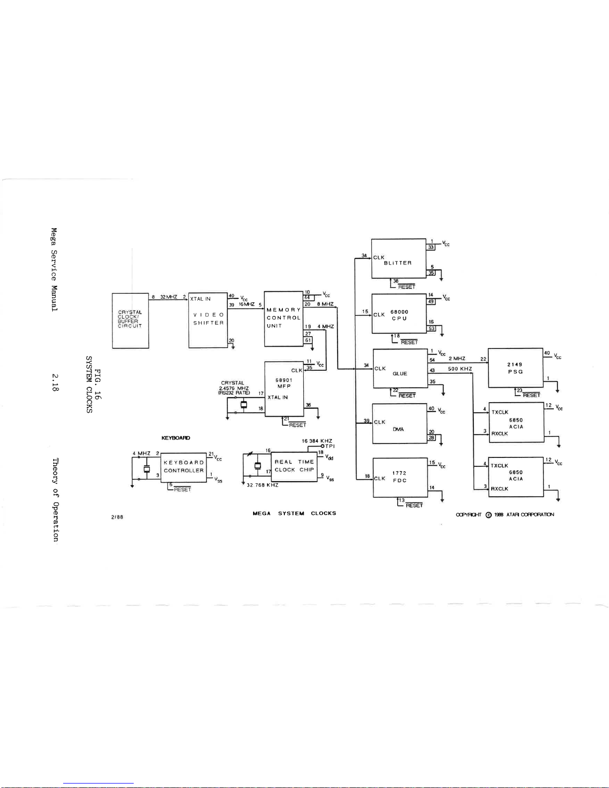
MEGA SYSTEM CLOCKS
BL¡TÏER
MEMORY
CONTROL
UNIT
XTAL
IN
VIDEO
SHIFTER
LK
68ooo
CPU
21 49
PSG
1772
FDC
Page 29

SECÎION
THREE
TESTING
OVERVIEI{¡
Ttris
section
pertains
to the test
equipment, diagnostic
software,
and test
procedures
used to verify
correct operation and
repair
the
Mega/ST
computers.
Tt¡e
diagnostic cartridge
should be
used if
possible.
If
the unit
gives
no
display
or
R5232
output
when
running
the cartridge,
see
rrTroubleshooting
a Dead
Unit'r
below.
Since
the
level
of
conplexity
in
the Mega/ST
systen is
high,
it
shouldn't
be expected
that this docunent
can
cover all
possible
problens
or
pinpoint
the causes; rather,
the intent
here is
to
give
a
systematic
approach which
a
technician
can use to narrolt
down
a
problen
to Íts nost
likely
source. Experience
in
troubleshooting
conputer
systems
is
assumed. Knowledge
of the
68000
processor
nay
be helpful. Economics
witl
be arì ínportant
consideration;
due
to the
low
cost
of the
Mega/ST
conputer line,
little
tine can be
justified
in
troubleshooting
down
to the
component
level
when
it
may be
cheaper to
exchange the
entire
sub-assembly. Many
of
the
¡nore
expensive
(and
critical) cotrponents
naybe
socketed,
naking
verification
and
replacenent
faster.
TEST EQUIPMEI.¡T
The following
equipnent will
computer:
be needed
to test the Mega/ST
i
Atari
SCl224 RGB Monitor
(or
sinilar)
i
Atari
SM124
Monochrone
Monitor
(or
siniJ-ar)
r
Atari
SF354 or
SF314
Floppy Disk
Drive
I
Mega/ST
Port Test Fixture
I
Mega
Expansion Test
Fixture
(Mega
only)
*
RS232
Loop-Back
Connector
t
MIDI Loop-Back
Cable
ì
Mega/ST
Test
Diagnostic
Cartridge
(Revision
4.0)
t
Diskettes
(2)
I
RS232
ternirral
(or
Mega in
tff52
enulator node)
In
addition,
the following
itens
will
be necessary
to
troubleshoot
and
repair
failed
computers:
r
0scilloscope
(100MHz
Recconmended)
*
Digital Multimeter,
1l
FS
(or
better)
*
Snall
Ha¡rd
Tool,
& Soldering
lron
*
Spare Parts
Mega
Service Manual
3.1
Testing
Page 30

TEST CONFIGI.JRATION
With the
power
switch
off,
Ínstall
the
Diagnostic
Cartridge
(IMPORTAI.IT--if
the
cartridge
does
not
have
the
plastic
enclosure,
BE SURE
THE
CARTRIDGE
IS
INSTALLED
WITH
THE CHIPS
FACINC
DOIW)
.
Connect
cables
fron test
fixture
into the
hard
disk
port,
parallel
port,
and
joystick
/
nouse
ports.
The
ioystick
cables
should
be
plugged
in so that,
if the
fixture
ports
were
directly
facing the
cornputer
ports,
the
cables
would
not be
crossed.
PIug the
R5232
and
MIDI
loopback
connectors
into their
ports.
PIug
the
color
nonitor
into the
nonitor
output
(a
nonochro¡ne can
be used
instead)
Power on the
unit. Some
tests
will
be
run autonatícally;
in
a
few seconds the
nenu screen
should
appear.
If
the
screen appeArs,
skip
down to
"
Mega/ST
Diagnostic
Cartridge
",
below.
If
not, read
next section
"Troubleshooting
a
Dead Unitrr.
If the unit
is being used
as
a terninal
for a
host computer,
it should
be disconnected
fron the
host before using
the
diagnostic;
otherwise,
the
host
nay think
soneone
is logging
oD,
and will send
nessages which
will act
like
keystrokes
input to the
diagnostic.
TROIJBLESHOOTING
A
DEAD UNIÎ
In the event
that
the
systen
is correctly
configured
and
pclwered
a¡¡d
no display
appears,
this
is the
procedure
to
use
for
determining
the
problen.
This assr¡nes
elementary
steps
have
been
taken,
such as
checking
the
LED in the
forward
left corner
of
the
compu+,er
to verify
the
unit
is
powered
and
naking sure
the
nonitor
is working.
1. Connect a
dumb terninal
to
the
RS232
port
of
the unit
under
test
(IJ.U.T.
).
You can
use an
Mega/ST
running the
l/T52
terminal
emulator
program--see
the
owner's
nanual
for
setting
up
tÆ52.
The
cable
should connect
pin
2
(serial
out)
of the U.U.T
to
pi.n
3
(serial
in) of the
terminal,
a¡rd
vice versa.
Connect
pin
7
(sround)
to
pin
7.
The terminal
should
be set up
for
9600
bps,
I
bits of data,
1 stop bit,
no
parity
(this
is
the
default
condition
for
the
VT)2 enulator).
Insert the
Diagnostic
Cartridge
into the U.U.T.,
8¡¡d
power
on
the unit.
If
the
Diagnostic
Cartridge
messages
appear
on
the
display of
the terninal,
use
the
diagnostic
to troubleshoot
tire
computer.
If not, the
conputer
will
have to be
disassenbled
to
iroubleshoot.
Refer
to
"Diagnostic
Cartridge"
below
for information on
using
the cartrÍdge.
If no activity
is
seen
on
the
RS232
port
or
display,
continue
with
(2)
next
page.
Mega
Service
Manual
3.2
Testing
Page 31

2. Disassenble
the conputer
so that the
printed
circuiÈ board is
exposed
(see
Section 4,
Disassenbly).
Power up the conputer.
Using
a¡¡
oscilloscope,
verify
the SMHz clock
to
the
68000
CPU
(pin
15).
Replace oscillator if necessary.
Tt¡en check
pin
17
(HALT)
of the
68000 CPU.
It
should be a
TIL
high. If so,
go
on ro
I
below. If
not,
the CPU
is halted. The
reasons may
be:
(1)
bad
reset
circuit,
(2)
doubte bus error,
3)
bad CPU.
Check
(1)
bV observing signal
on
input
of the tn¡o
inverters
on
the
HALT line. Check
(2)
by
observing
pín
22
of the CPU
(BERR)
as the unÍt
is
powered
on. It
should be
high
always.
If
there
are
logic low
pulses,
some
conponent is malfunctioning
a¡¡d
Glue is
generating
the error.
Verify the clocks to GIue a¡rd Menory Controller
and
replace
these
conponents
to verify then
(if
socketed).
If
still failing,
the CPU
is
unable
to
read ROM or there is a
conponent wlr-leh is not
responding
to a
read or write
by
the CPU,
probably
the
MFP
68901
or DMA Controller. The
MFP
should respond to
an
MFPCS
with DTACK.
The DMA
chip should
respond
to
FCS
by asserting RDY. There is
no
way
to check
(3)
other
than by elinination
of the other
two
possÍbilities,
although a
hot CPU
(too
hot
to touch for nore
than
a
second)
strongly
indicates
a bad
CPIJ.
3.
If
the CPU
is not halted, it
should be reading instructions
f'ron ROM
(cartridge,
if installed)
and data a¡¡d address lines will
be toggling.
(If
not, replace CPU. ) At this
point,
there
is
the
possibility
that both
the video
and
RS232
subsystems are failing.
Verify the output of the
MFP
chip
(pin
8)
while
powering
on the
unit with
the cartridge
installed. If
data
is
being sent. trace it
through the 1488 driver.
Note
that
+
a¡rd
-
12v. is required for
RS232.
If
all
looks
good,
there nay be sonething
wrong with the
connection
to the
terninai.
Verify also the output
of the
Video Shifter.
If
using an RGB
nonitor,
check the outputs to the sunnirrg
resistors
(if
external)
for R,
G, a¡¡d
B. Note
that
if BLANK is not
going
high, no
picture
will be
possible.
If using nonochrone,
check output
pin
30.
AIso
check
the
input
to the
MFP,
pin
29, M0N0M0N. Note
that
if
the CPU
does
not
read a low on this signal on
power-up,
Ít will
cause
RGB
output
on the Video Shifter.
If
the
Video Shifter
is outputti.ng a signal, but
the
picture
is unreadable,
there
is
probably
a
problen
with screen RArY. The
cartridge should be used to diagnose this
problen,
with
the
RS232
terminal
as a
display
device.
Mega
Service Manual
3.3
Testing
Page 32

MEGA/ST
DIAGNOSTIC CARTRIDGE
The
diagnostic cartridge
is used to detect a¡rd isolate
conponent failures
in
the conputers
(52O/LO4O
and Mega). There
are
several
revisions;
this docunent
refers to
revision
4.0. Users of
earlier
versions
should
refer to the appropriate
Troubleshooting
Guide. This section
gives
a brief
guide
to use with a description
of each test, error codes
or
pass/fail
criteria, and
recommendations
on
repaír.
Power-up
The
diagnostic
program perforns
several tests on
power-up.
In
particular,
the
nessage
"Testing
MFP, GIue tining,
Video will
appear,
a¡rd the screen will appear scrambled
for a few
seconds
before the
menu is
printed.
The screen will
turn
red
(dark
background in nonochrone)
if
a¡r emor occurs
in
the
initial
testing, with a
message indicating
the
failure. The lowest
2
Kbytes of RAIü is tested on
power-up;
if
a
locatíon fails,
the
error wiII be
printed
to the
R5232
device.
It is
assumed that
if
RAM is failing,
Lhe
screen nay not be
readable
a¡¡d
program
execution will
fail
because there
is no
stack
or
system variables.
The
progra¡n
will continue to test
RAM and
print
emors, but
no
screen will be displayed
(the
screen
¡nay turn
red).
Repair RAM.
If
the
keyboard fails, it will
be
inactivated. The
user nust
connect
a
terninal to the
R5232
port.
The
diagnostic
progra¡n
looks
for keystrokes fron
the
RS232
device.
If
the display
is
unreadable,
the
RS232
terminal should be
used.
All nessages
are
printed
to the
R5232
port
as
weII
as the
screen.
Test Menu
The normaL
screen will be dark blue
with white letters. The
test title and
revision nunber
are displayed at the
top,
with the
anount of
RAM
and
keyboard
controller
revision below, and a test
menu
below that.
To
select tests, the user types the
keys
corresponding to those tests, and then the
return key. Many
iterations of the test or tests chosen ca¡r be
run
by typing
in
the
nunber
of cycles
just
before typing RETURN. Typing a zeto will
cause the test sequence to
run continuously. To
stop a cycle
before
completion,
hit the
escape
key
(there
nay
be sone delay
in
sone tests before
the
test
stops). As
each cycle conpletes, the
total
numbers of cycles will be
displayed
on the screen.
Mega
Service
Manual
3.4
Testing
Page 33

MAIN
MENU
Mega
and
4u
nnu
ST
Field
Service
Diagnostic
Test
Rev'
4'0
o
1987,
Atari
CorPoration--
Keyboard
revisioi-V----6O
n"
0S
Version
2
USA
NTSO
c
S
D
H
R
K
A
F
G
L
X
0
z
E
B
V
?
RAI{
Test
0
0'S'
ROltls
Keyboard
M
MIDI
Audio
T
Timing
Fioppy
Oisk
P
Printer/JoY
Ports
Graphics
chiP
(Blitter)
ReaI-tine
clock
Expansion
connector
Run
AII
Tests
iun
rnternal
tests
(R,o'c'K'A'T'L'G)
Exanine/ModifY
nenory
Set
RS2l2
rate
iãÀgr"
iia"o
outPut--5o/6o
Hz
Help
Enter
letter(s),
and
REIURN
ons
will
be
highlighted
if
these
e.
These
should
be
Present
in
tion
requires
the
exPansÍon
test
quires disassemblY)
'
If
these
ishted,
the
test
wirl
check
for
hrough
all
the
tests
except
for
seleðtion
sequences
through
RAM'
tests.
Selection
'E'
enables
the
or
hardware
registers'
The
'B'
e
baud
rate
on
the
RS232
Port'
Pressing
the
up
arrovJ
increases
it'
pressing
the
down
arrovr¡
decreases
it.
Pressing
'?'
or
the
HELP
key
brings
up
a
brief
synopsis
of
the
cartridge
functions.
After
a
test
or
series
of
tests
conpletes'
the
pass/fail
status
arrA
er"ãr-".po"t,
if
any,
will
be
displayed'
Press
the
space
bar
to
return
to
the
nenu'
If
nultiple
tests
are
selected'
the
sequence
can
be
halted
before
completion
by
pres"ins-ihã
BéC
tey.
Át
ttte
conpletion
of
the
current
test,
the
sequen"å
"iff
hali,
with
the
options
of
either
continuini
or
returning
to
the
nenu'
In
some
cases
there
will
be
"
"or,"id"iabte
delay
Uãfore
the
current
test
conpletes
and
rhe
keysr"oL"
i"-ããlãðt"0.
iup-lã
i
minutes
with
4
meg
of
RAM'
)
CoIor
Serial
Port
DMA
Port
High
resolution
Mega
Service
Manual
3.5
Testing
Page 34

Sumnary of
Tests
RAM TEST
RAM is tested
in
three stages:
low
2 kbytes,
niddle
(up
to
64t¡, a¡rd
fron
64t
to top.
The test
patterns
used
are: all ls, all
0s, a counting
pattern
(data=low
word of
the address)
'
reverse
counting
pattern (data=conplenent
of address
low
word).
The
counÈing
pattern
is copied
fron the top
and
botton of a
J2
Kbyte
buffer
into
the current
J2
Kbytes
of
video
RAM, then shifts video
RAM
to a
new
area,
verifies
the
pattern,
and
repeats
the test,
until the top of
RAM
is reached.
Finally, addressing at 64t
boundaries
is
checked
by writÍng
unique
pattern
in last 216
bytes
of
each
64t Utoct.
If an error occurs,
the error
code
is displayed, followed by
the address, data
written,
data
read, and the bits which did
not
agree.
E.g.:
"
R2 45603E W:603E
R:613c bad bits:
1,8".
In
units
having nore than one ba¡rk
(i.e.,
1040ST, MEGA4)
the
address as
well as the bit
position
nust be used to find the
correct chip.
The following table
gives
a
correspondence between
the addresses and banks
for
various
models:
520
O-7ffff
bank 0
Soooo-rrrrr
100000'lfffff
200000-3fffff
1040
bank
0
bank
1
Vlega
2
bank
0
barrk 0
bank
0
Mega
4
bank 0
bank
0
bank 0
bank 1
(A
bank
is
a
16 bit wide
group
of RAMs.
A bank
nay
consist
of 256k
bit
chips--256k
x 16
=
4
UUit or
JL2k
bytes--or
lMbit chips--lMbit
x 16
=
16 Mbit
or
2 Mbytes.)
RAM ERROR CODES
Except where
noted,
repair by
replacing the
RAM
chip
corresponding to the
indicated bit(s).
R0--1ow nenory failed while setting
up to
run
test.
Rl--failed walking
1s
or 0s.
R2--failed
address
(counting pattern)
.
RJ--failed
64t< boundary
test.
Probable failure
in
Controller.
n4--failed
while displaying area
tested
(video
RAM).
Memory
Mega
Service
Manual
3.6
Testing
Page 35

ROM TEST
Ttris
test reads
the configuration
bytes
of the operating
systen to deternine
the version, tanguage/country,
and
TV standard
(PAL
or
NTSC).
AII bytes from
operating
system
ROMs
are then
read
and the checksuns are
calculated.
These
values are conpared
against known
value
with
checksuns for
this version
to
deternine
if
good
or bad.
Six checksuns
are displayed,
although
there
may
be only
two
ROMs
in
the machine
(sone
machines have six
128K
ROltls;
sone have
two
1
neg ROM'S).
The
test fails if
the
checksun calculated does
not natch
the
checksun expected for
the configuration
byte
found
(e.S.
Version
2, French).
Incorrect
checksums are
indicated
by a
nessage. If
an
error is
displayed, replace
the correspondÍng
ROM. In
a two
ROM
set,
replace
the
low ROM if
any of
L0, L1,
or
L2
showed an
error,
or replace
the
high ROM if
any of H0, H1,
or
H2
showed an error.
New
revisions of
T0S
witl cause this
test to
fail if
not
incorporated
into the current version
of the diagnostic. If
you
receive T0S revisions
before
receiving
the
diagnostic revision,
it
will
be
necessary
to
verify
the
checksr¡¡ns
yourself.
COLOR TEST
This
test verifies the Video
Shifter. Seven color ba¡rds are
displayed:
red,
green,
blue, cyan, nagenta,
yellow,
and white.
Each
band consists of 8
leve1s
of
intensity. All
16 color
palettes
are represented, each
palette
is
a vertical strip across the
screen
(strips
should
not
be discernable, but each color
should
be
a straight
líne
across
the
screen).
Because
of the tight tining
involved,
keystroke
intemupts
will
cause
the display
to
jitter.
The
operator
should see
that
there
are
no
gaps
or
missing
sca¡r
lines in
the display.
If lines
are
nissing,
check the three
outputs on the Video Shifter for that color, and verify the values
of the resistors on the output. Too
low
a brightness setting on
the nonitor
will cause
the
nonitor
not to distinguish between fine
levels, making it
appear there are only
four levels
being output.
The
Video Shifter
has three
outputs
for red
(R0,
R1, R2),
green
(G0,
G1, G2)
and blue
(80,
81, B2l. Each
of
these
triples
is
sunmed together by a resistor network to
give
eight levels of
intensity for
each color,
depending
on which of the outputs are
on.
The
values of the
resistors
give
different weight to each out-
put.
The
value of the
resistor
at
R0
is twice that of R1, which
is
twice that of
R2. This
allows us to
get
8 equal steps on the
sumned outputs. For exanple,
R0
on
,
R1
and R2 off
=
L/8, R0
off,
Rl and R2 on
=
7 /8.
this
signal then
passes
through a transistor
anplifier,
and
fron there to the video
nonitor
connector.
NOTE :
this resistor
network is incorporated into the full custon chip
in
later versions of the video shifter
(C101608).
Video shifter
which has
part
nunber C101608
or CO7O7I3
has
pin
1
connected
to
to
signal
line BLANK. Shifter with
part
nunber CO259I4 will
have
pin
1 connected to a
pull-down
resistor R144,10K,
and signat
line
BLANK
will be connected
to diodes D9, D10, D11.
Mega
Service
Manual
3.7
Testing
Page 36

Symtons
and
fixes:
1.
Missing
prinary
color.
Check
the
output
of the transistor
anplifier.
06
is
blue,
Q7
is
green,
Q8
is red. Look for a
staircase
pattern
(eight
levels
of
intensity).
If the
signal
is
there,
trace
forward to the
video
connector,
if
not,
trace
backward
to the
Video Shifter,
until
the
faulty conponent
is
found.
2.
Prinary colors
present,
secondaries
níssing or
incorrect.
Replace the
Video Shifter.
3.
Coarse
change
in intensity
(not
a snooth
dark to
light
tra¡rsition).
Replace
Video Shifter
or
look
for
a short
on the
output
of one
of the three
color
outputs
for
the appropriate
color.
4.
Specks or
lines on the screen.
This
can
be
caused
by bad
RAM;
if RAM
has
been
tested
a¡rd
is
good,
replace the Video
Shifter.
5.
Wavering
display,
horizontal
lines
not
occurring
in
the
sane
place
every
tine.
The
processor
nay be
getting
extra
interrupts
(if
the
processor
is required
to handle additional
interrupts,
it will
not
have
tÍner
to change aII
L6
color
registers
during a
horizontal
scan
time).
Exanine
the
MFP
interrupt
request
(pin
32).
There should be an
interrupt
every
L26
mícroseconds
(2
display
lines)
fron Display
Enable
(pin
20). If additional
interrupts
occur, locate the
source:
the
inputs at
pins
22-29 should all
be
high. If
no
external
(to
tne
Ufp) source
for the
interrupts
is found,
replace the
MFP.
NOTE: if the
keyboard
is
not
connected,
the
input to the 6850
will be
low, causing
continual
intemupts.
KEYBOARD
TEST
Two types
of test are
run.
The keyboard self-test
is
done
first, and
if this
passes,
a screen
is displayed
representing
t'he
keyboard.
If multiple tests
have been selected,
only the self-test
is run.
The operator
presses
keys and observes
that
the
comesponding
character
on
the
screen
changes
(reverses
background
color).
The key
will also
be displayed
in the
lower half of the
screen.
The
mouse
buttons a¡rd
four directions are also
shown
on
the
screen.
Connect
the
mouse
and
nove
in
any direction
a¡rd the
arrow
will
flicker.
Any key clicks while the
¡nouse
is noving
indicates
a short.
The self-test
checks comnunication
between
the
CPU and
the
keyboard
nicrocomputer,
and
checks
RAM and ROM
in the
keyboard
microcomputer,
and scans
the keyboard
for stuck
keys.
Mega
Service
Mar¡ual
3.8
Testing
Page 37

KEYBOARD ERROR
CODES
KO--stuck
key. A key
closure
was detected whire
the keyboard
self
test was
executing.
K1--Keyboard
not responding.
A
connand
nas
sent to
the keyboard
processor
and no
status
was returned
within the
allowed
tine. Ttre
keyboard
needs
to
be
replaced
or the connunicatÍon
channel
through
the
6850 is not functional.
K2--Keyboard
status
error. The
setf test
coûDand was
sent
to the
keyboard,
on conpletion
of
the
test,
the
keyboard
sent
an
error
status. Replace
the
keyboard.
MIDI
TESTS
This
test
sends data
out
the MIDI
port, (data
loops
back
through
the cable)
a¡rd reads
fron
the input
and verifies
the data
is
correct. This
also
tests
the interrupt
fron
the
68J0
through
the
MFP
chip. The LED
in
the loopback
cable will
brink
as
data is
sent
(not
all cables have
the LED).
MIDI
ERROR
CODES
MO--Data
not received.
Trace
the signal from
the
output
of
the
6850, through
the drivers,
loopback
cable,
and
receivers
to the
input
of the 6850. Replace
the defective
component.
M1--ldrite/Read
data nisnatch.
Ttre
data b'ritten
was not
the
same as
the data read. Replace
6850.
M2--Input
frane
error.
ga¿
6850 or bad driver
or receiver
causing
noisy
signal
MJ--Input
parity
error.
ga¿
6850 or bad driver
or receiver
causing
noisy
signal.
M4--Input
data
overrun. The
6850 received
a byte before
the
previous
byte
was
read.
Probable
bad
6850,
also
can
be caused by
the MFP
not responding
to the
interrupt
request.
Mega
Service Manua1
3.9
Testing
Page 38

RS232
TESTS
t'irst the
RS232 control
lines
are
tested
(which
are tied
together
by the
loopback
connect,or),
then
the data
loopback is
tested.
Data
is checked transnissing?receiving
using a
polling
nethod
first, then
using
interrupts.
Data
is transnitted
at
300,
600,
LãOO...t92OO
bps.
Data
tra¡rsnission
is
perforned
by the
MF?
and
the
1488
and
f489 driver
and
receiver
chips.
Interrupts
are
a
function of the
MFP. Control
lines
are output
by the
PSG chip and
input on the
MFP.
Note that
this
test
does
not
thoroughly
test
the
drive
capability
of the
port,
as the
RS,232 device
nay
requÍre
voltage
swings
of
12 volts
& there
are
no
load resisters
in the serial
port
diagnostic
connector.
If
the
test
passes,
but the
unit
fails
in
use,
it is
likely that
the
1488 or
f489
cfrips
are
bad.
R5232
ERRoR
CoDES
Data transmission
error:
S0--Data
not received.
Check signal
path:
MF?
pin
8 to J6
pin
2
via
1488 to J6
pin
3
to
MFP
pin
9
via
1489.
Sl--Daca
nisnatch.
Data read was
not what
was sent.
Check
integrity of
the signal.
May be bad
driver,
receiver,
or
MFP.
S2--Input
frane
error.
Incorrect
tine between
start
and stop
bits.
Probable
MFP failure.
S3--Input
parity
emor.
Input data
had
incomect
parity.
Probable MFP
faÍIure.
S4--Input
data overrun.
A byte
was
received before
the
CPU read
the
previous
byte.
MFP failure or,
less like1y,
GIue
failure.
S5--No
IRQ. CPU did
not detect
an
interrupt
by the,MFP.
MFP
or
GIue failure.
S6--Tra¡rsmit
error.
MFP
transnitter
failed.
S7--Tra¡rsnit
error
interrupt.
An
error
condition
was ereated
intentionally
to cause
an
interrupt,
and
MFP didn't
respond.
S8--Receive
error
interrupt.
intentionally to
cause
an
respond.
An
error
condition
h,as created
interrupt,
and
the
MFP did
not
S9-'RI/DTR
connection.
Signal
sent at
DTR
is not detected
at
RI.
SA--DCD/DTR
connection.
Signal
sent
at
DTR
is not detected
at
DCD.
SB--RTS/CTS
connection.
Sig¡al
sent
at
RTS
is not detected
at
CTS'
Mega
Service
Manual
3.
10
Testing
Page 39

AUDIO
TEST
Outputs
a low
to high
sweep on each of the three
sound
channels.
One cycle
of each cha¡rnel
is
perforned.
If
a
channel
is
nissing, replace
the
PSG
chip.
If
no sound is heard,
verify the
output
of the
chip wÍth an oscilloscope,
and trace the
signal
to
the
nonitor
output
connector.
If
no output from
the
PSG,
verify
the
PSG
Ís being
selected
by
running
the
printer
port
or
RS232
test
(these
tests
both select the PSG).
TIMING TESTS
These
tests
are
run
at
power-up
as well as
being selectable
fron
the
nenu.
Ttre MFP
timers, the
GIue
tining for
VSYNC a¡rd
HSYNC,
a¡¡d the Menory Controller video
display
counters are
tested. Tt¡e
video display
test
redirects
display nenory
throughout
RAIII
a¡rd
verifies
that
the correct
addresses are
generated.
Odd
patterns
nay flash
on screen as this test is run. Tt¡ere
are
two
tests
which
check the bus timing
for
the
1772
and
PSG
chips. An
error
Dessage
is
printed
to the screen,
then the test is run. If
the test
passes,
the
nessage
1s
erased.
If
not, a Bus Error
will
occur
and the nessage will renain. If
a terninal is
connected to
the
RS232
port,
the
nessage
will
not
be erased,
but
'rPass"
will be
printed.
TIMING TEST ERROR
CODES
TO--MFP
tiner
error.
One
or
nore
of the
four
tiners in the MFP did
not
generate
an
interrupt
on counting down
Tl--Vertical
Sync.
GIue is not
generating
vertical-
sync
in
the
required
tine
period.
T2--Horízontal
Sync. Glue
is not
generating
horizontal
s¡mc
in
the
required
time
period.
T3--Display
Enable. Glue is not
generating
DE
output
or
the IIIFP
is
not
generating
an
interrupt.
t4--Video
Counter Error. The nenory
controller is not
generating
the correct addresses
for
the display. This
will
result fn
a
broken-up dÍsplay in
sone or all display
nodes.
.-
f
ruu
lt)
T5--PSG
Bus Error. Ttre PSG
chip
is
defective.
T6--L772 Bus Error. The LlJ2
chíp
is
defective.
Mega
Service Manual
3.11
Testing
Page 40

\/o'
DMA TESTS
Four
sectors
(2048
bytes)
of data
are h¡ritten to the RAM
on
the
port
test fixture via high speed
DMA,
then
read
back a¡rd
verified. Tt¡is test Ís
repeated nany
tines
for RAIII
addresses
throughout the
rarìge
of
RAM.
DMA TEST ERROR CODES
DO--DMA
tined out.
No DMA
occurred due
to faulty DMA Controller,
GIue, or
Memory
Controller, or the
HDII{Î interrupt was not
processed
by the
MF?.
The failure can be
isolated
by seeing
íf
the
DMA Controller responds to
HDRQ fron
the test fixture
with
ACK.
Verify the
MF? by seeing that the HDII{T input
causes
an
INTR output fron the
MFP.
D1--DMA
counter error.
the nunber
of bytes transferred was
incorrect. The Menory Controller or
DMA
Controller is bad.
D2--Data nisnatch
emor.
Ttre
data
received fron
the
DMA
port
was
not
the sa¡De as the data sent.
Replace
the
DMA
Controller. If
the
problen persists,
check the
data lines
to the
port
for
opens a¡rd shorts.
A
third
possibility
is
that a defective
7lJ2 is
loading the bus.
D3--DMA not responding. DMA
controller
could not respond
to a data
resquest fron
the external controller.
Replace
the
DMA
chip.
FLOPPY DISK
TESTS
The Floppy Main Menu
Floppy
disk drive
routine
(I{ARNING
--
all choices
except
2,6,7
write to the disk)
1)
Quick
Test
2) Read Alignnent Disk
3)
Disk
Interchange
Test
4
)
oist<
E;<erciser
5)
Check copy
protect
tracks
(80-82)
6)
Test
Speed
7)
InstaII
disk dríves
In
single test
noder
a
r¡enu is displayed showing seven options:
1.
Quick
test.
For
each
disk
installed, fornats,
writes, and
reads
tracks
0,
L,
and
79
of side 0.
If double
sided,
fornats
a¡rd
rvrites
track
79
of side
1
and
verifies
that side 0 was
not
overwritten.
If
no
disks are
installed,
checks to see what
drives are online and
if
they are
double or
single
sided.
To
assure that the drive are correctly tested, the
operator should
install
(nenu
option 6) before calting the
test. Once the
test is
run,
the drives become
installed,
and
will
be
displayed on the nenu screen
(below
the
RAM
size).
Mega
Service
Manual
3.72
Testing
Page 41
Read
track.
Continuously reads
a
track,
for checking
alignment
with an analog alignnent
diskette.
The
track
to
be read
nay
be
input
by the
operator.
If
"Return"
is
pressed
without entering
a nunber, the default
is
track 40.
Interchangeability test. Checks to see
if diskettes
fron two
disk drives each can be
read
by the other
disk drive.
4.
Disk exerciser.
A nore
thorough disk test;
tests all
sectors
on the disk
for
a¡r
indefinite
period
of tine.
Copy Protect Tracks. Tests tracks 80-82,
which are used
by
some
softrùare conpanies for
copy
protection).
Not all
failures
are cause
for replacenent because sone
nanufacturers disk
drives will
not
write to these tracks.
Test speed.
The rotational speed of the drive
Ís tested and
displayed on the screen
as the
period
of
rotation.
The
acceptable
range is
196-204 nitliseconds. The híghest and
lowest
values
measured are displayed.
The
test stops
when any
key is
pressed.
InstaII
disks.
Specify
how nany and what type of disks to test.
If nore
than
one test
is
selected
from
the
nain nenu, the
floppy nenu will
not
appear,
but the
Quick
Test
will be selected
autonatically.
FLOPPY TE.ST ERROR
CODES
No floppies connected--the
controller
cannot
read
:Lndex
pulses.
The
cable
nay be
inproperly connected,
or the clrive
has
no
pohrer,
or the
drive
is faulty.
F0--Drive
not
selected.
Drive
was
installed, but
failed attenpting
resLore
(seek
to
track 0).
Check cornection of cables,
pourer
to drive. Verify
the
light
on
the
front
of the
drive
goes
on.
Listen for the sound
of the
head
seeking
(the
slide
on the
diskette should
open).
If
all
this occurs,
TRO
(pin
23
on
the
1772')
should
go
Iow.
If
so,
check
for
an
interrupt on
pin
28
of the
7772. If
none, replace the
1772. Else trace
the
interrupt to the
MFP,
verify
that
the
MF? responds be
asserting
INTR.
If the drive
is not being selected
(no
light), check the
PSG chip.
Pin 20 should
go
low when drive
A
is
selected, and
pin
19
should
go
low when drive
B
is
selected.
If
not, replace the
PSG.
F1,F2,Fl errors of
previous
versions
have
been
deleted.
The error
nessage now says
"Error
liriting"
(or
reading or
formatting),
and displays
a
nore
specific
emor
nessage, €.8.,
"F9
CRC
errortt.
2.
3.
5.
6.
7.
Mega
Service
Manual
3.
13
Testing
Page 42

F4--Seek
error.
Verify that the
STEP,
MO,
and
DIRC
outputs
fron
t,l:e
1772
are
sent to the drÍve. Probable failure
in
the L772,
but
the drive is
also suspect.
Fl--lirite
protected.
Check the
write
If
0K, verify
that the ldP input
during
the test; if it is,
then
not,
the
problem
is
with the
disk
protect
tab on the
diskette.
(L772 pin
2l) is
going
low
the 1772 Is
defective;
if
drive.
F6--Read
compare
error. Data read
from
the
disk
was not
what was
supposed
to be
written. Check in
the following
order:
diskette,
disk drive, L772,
and
DMA Controller.
F7--DMA
error.
DMA
Controller
could
not respond
to a
request
for
DMA. Replace
the
DMA
Controller. If
emor
persists,
check
FDRQ
whÍle running
the test. It
should nornally
be low
and
go
high
with
each data byte
transfemed. If
stuck high,
push
the
reset
button
a¡rd verify
that
MR
(L772
pin
13)
goes
low.
If
not,
trace RESHI
to
its
source.
If MR
is
0K, but FDRQ
is
still stuck, replace
E}r'e
1772.
F8--DI{A
count
error. Replace
the Memory
Controller,
not fix
it, replace
the
DMA
Controller.
if
that does
F!--CRC
error. The
diskette
or disk
drive
nay
be bad,
else replace
Ehe 1772.
FA--Record
not found.
The L772
could not read
a
sector
header.
May
be
a bad diskette,
drive
or
L772. If
the test. fails
drive A
but not
drive
B,
Ehe
1772 is
not
at
fault
(likewise
fails
B
not
A).
FB--Lost
data. Data
was transferred
to t}:e L772 faster
than the
1772
could tra¡rsfer
to the
DMA
Controller. If DMA
Port
test
passes,
the tJl2 is
probably
bad.
The DII{A
Controller
could
also be
at
fault.
FC--Side
select
emor--single sided
drive. The test tried
to
write
both
sides of the
diskette, but writing
side
1
caused side
0
to
be overwritten.
FD--Drive
not ready.
The fornat/write/read
operation
timed-out.
Probably
a
bad disk drive. Verify
by checking
another drive.
Could
also be a faulty L772.
Soft Error
=
does not
cause a failure
after 1 retry.
(If
doesn't
fail
a second time.
)
Hard Error
=
failed
second
retry.
Unit
will
halt if
you
reach any
of the
following:
20 read
errors, 20
write errors or
!
fornat
errors.
Mega
Service
Manual
3.
14
Testing
Page 43

PRII.ITER AND
JOYSTICK
PORT TF"STS
The
port
test
fixture
is
used to test
the
paralle1 printer
port
and
joystick
ports.
The
parallel port
test
writes
to
a latch
on
the test
fixture and reads
back data.
The
joystick
port
test
outputs data on the
parallel port,
which
is
directed through
the
test fixture
to the
Joystick
ports.
The keyboard
reads
the
joystick
data
in response
to connands
from
the
CPU. The
cables
connecting the
joystick
ports
to the test
fixture nust not be
reversed,
or the
printer
and
joystick
tests will
fail.
PRTNTER/JoYSTTCK ERRoR CoDES
Po--Printer
port
error.
Data read fron the
printer
port
was
not
what was written. Verify that
the
data
lines
on the
PSG
chip
(pins
6-13) are toggling
when
the test
is run. If not, run
the RS232 test.
If
the
RI-DTR
and
DCD-DTR
errors occur, the
chip
is
probably
not being
selected.
Check if
the chip
-
selects are being activated
and
the
2ütlz
cLock
is
present.
If
the
PSG is
selected and
not
outputting signals,
replace it.
If
the data
lines toggle, verify
continuity.
AIso verify
that
J1l
(Joystick
0)
pin
3
is
pulled
up. Verify the test
fixture
is
good
by testing
another conputer.
If it is
0K,
replace
the
PSG.
P1--Busy input
error.
The
input
to the
MFP is
not being
read,
or
the STROBE output
fron
the
PSG
is not
functioning, or
Joystick 0
pin
I
is not connected.
If
the
P0
error also
occurs, see
handling
for
that. Othervise,
look
for
a signal
amiving at
MFP
pín
22 fron
J5
pin
11. If no signal at J5,
the test
fixture may be bad. Verify
with
another conputer.
JO--Joystick
Port
0.
Ttre
keyboard input is not functioning. If
the
Busy input
error occurs,
fix
that
first.
othervise,
replace
the
keyboard. If error
persists,
check continuity
fron J11
pins
1,2,3,4
to ltZ
pins
12,10,9,8 respectively.
Jl--Joystick
Port 1. The
keyboard input is not functioning. If
the
Busy
input error occurs,
fix
that
first.
otherwise,
replace
the
keyboard. If
error
persists,
check continuity
fron J11
pins
1
,2,3,4
to ttZ
pins
J,5,4,1
respectívely.
J2--Joystick time-out.
Joystick
inputs
rdere si¡rulated
by
outputting data on the
printer port
and routing Ít via the
test fixture to the
joystick
ports.
Joystick
inputs
are
detected
by
the
keyboard and sent to the CPU via the 68¡0.
This
error ca¡¡ be
caused by
printer port
failure
(code
P0),
keyboard faílure,
keyboard-CPU connunication line, or a
faulty
test
fixture.
If
the
porter-up
keyboard
test
passes,
this elininates
any
problen
with
keyboard-CPU
communication.
Mega
Service
Manual
3.r5
Testing
Page 44

J3--Left
button
input.
If Pl emor
occurs,
fix
that
first.
0therwise
replace
the
keyboard.
0n the
520ST,
also check
continuity
from J10
pin
6 to ltZ
pin
11.
J4--Right
button
input.
If
Pl
emor
occurs
,
fix
that
first.
Otherwise
replace
the
keyboard.
0n the
520ST,
also check
continuity
fron J10
pin
6 to JtZ
pin
6.
HIGH RESOLUTION
MONITOR
If this test
is selected
while a color
monitor
is
connected,
a
message
is
displayed
to
connect the
nonochrone nonitor. The
CPU
waits
for an
interrupt
from the
MONOMON
input
to the
MFP, and when
received
(the
operator
connects the
nonochrone
nonitor),
changes
the
dÍsplay to
high
resolution.
Ttre display screen shows
horizontal and
vertical
lines, each
2
pixels
in
width.
Ttre
screen
will
reverse every
two seconds.
ltlhen the
operator sees the display
is
correct,
he
unplugs
the
nonochrone
nonitor and
re-connects
the
RGB
nonitor
a¡rd
the display
should
return
to
nornal.
GRAPHICS
CHIP
(BLiTTER)
This tests the
abÍIity
of the
BITBLiT to
Eove blocks
of nenory
around and
perform
logical operations
on the
data.
No
patterns
appear
on the screen.
Ma¡ry different
error
messages are
possible
(G0-G13)
,
but the
action
for
any emor
is the sa¡ne:
replace the
chip.
A faulty
BLiTTER
may
cause
a
BUS
ERROR.
REAL-TIIúE CLOCK
The test saves
the
current
time and
date,
and writes a
new
time, waits
one second,
and
verifies
that
hours,
minutes, seconds,
etc.
have all
rolled over.
The
is repeated
for a¡rother
date to
verify all
registers.
EXPANSION
CONNECTOR
This
test,
for
Mega
modeJ.s,
requires the expansion
test
fixture
(the
top cover
and shield
must be
renoved to
install Èhe
test
fixture).
It tests the
expansion
interface,
in
part
by
software,
and
the
renainder
by LEDs.
The data and
address busses
and
interrupt
lines are tested
in
software.
The
control
lines fron
the CPU are
tested
with the
LEDs.
Most of the
LEDs will
go
off
after
the systen
is
turned
on and
the
Inenu appears on the
screen.
Three LEDs will
remain
lit:
BR
(bus
request),
BG
(bus grant)
and
BGACK
(bus
grant
acknowledge).
These should
go
off after
(1)
the
expansion
connector
test
is run
and
(2)
either
the
DltIA test or
floppy test are
run.
The LEDs sinply
indicate that
the
line is
toggling.
A lit LED
neans the
line
is not changing.
Mega
Service
Manual
3.t6
Testing
Page 45

The software
tests
three
groups
of
signals:
data
bus, address
bus,
and
interrupts.
The first
test
writes
and
reads the
RAM on the
test
fixture,
setting
one bit
high
at a
tine, to
check
for open
or shorted
data
lines. If an
error
is found, the
nessage
"EXO
bad
bit"
is
displayed.
The second
test
writes an
increnenting
pattern
(0,1,2,...1
across address
bits
O-1!, then
across
address
bits
16-23 to
the
RAM
on
the test
fixture to check
for open or
shorted
address
bits.
If an error
is found, the
message
"EX1
external
RAM error'
low
byte" or
I'EX2
external
RAM emor,
high byte"
is
printed,
depending
on
whether
the error
occurred
in
the
low or
high address.
The third test
uses
circuitry
on the
external
test
fixture
to
create
interrupt
requests.
There
are
three
interrupts:
Il.¡T3,
IlfT5,
and
INT7.
If the
appropriate
interrupt
does
not
occur
when
expected,
then a
nessage Ís displayed:
"EX3
INT3 error,
"EX4
INT5
errort',
or
ttEXl
INTJ errortt.
ERROR
CODES
QUICK
REFERENCE
Ttris
is a
brief
sunmary
of
all error
code
which
nay
occur
when
running the
diagnostic.
INITIALIZATION
(Errors
occurring
before
the
title and
menu appear)
11 RAM
data
line
is stuck.
L2 RAM disturbance.
Location
is
altered
by write
to another
5
V*,
location.
13
RAM
addressing.
Wrong
location
is being
addressed.
14- MMU error.
No
DTACK after
RAM access.
I5
.
RAM
sizing
error.
Uppernost
address
faiLs.
T6-
EXCEPTIONS
(may
occur
at any
tine)
El--E5
not used
E6 Autovector
error.
IPLO
is
grounded
or 68000
is bad.
E7 Spurious
interrupt.
Bus
error
during
exception
processing.
Device
interrupted,
but did
not
provide
interrupt
vector.
EB Internal
Exception
(generated
by 68000).
E9 Bad
Instruction
Fetch.
EA Address
error.
Tried
to
read
an
instruction
from an odd
address
or
read or write
word
or
long word at
an odd
address.
Usually
this error
is
preceded
by a
bus emor
or bad
instruction
fetch.
.--EB
Bus error.
Generated
internally
by
the 68OOO
or
externally
by
GJ-ue. Usually
caused
by
device
not responding.
Displays
the
address of
the device
being accessed.
tr
rrirl-
6
LU
!
/
¡'')
,t
u¡ò1
i4
"¡4
tJ
Mega Service
Manual
3.17
Testing
Page 46
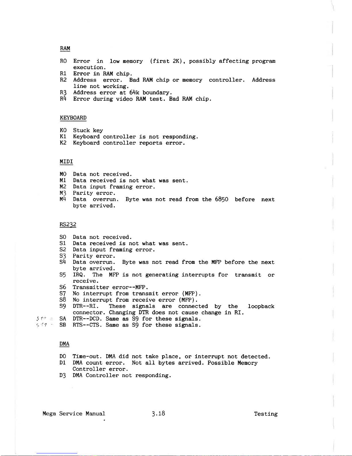
RAM
R0 Emor
in
low
nenory
(first
2K),
possibly
affecting
program
execution.
Rl Error
in RAM
chip.
R2 Address
error.
Bad RAItl
chip
or
memory
controller.
Address
line
not
working.
R3 Address
error at 64k boundary.
R4 Error
during
video
RAM test. Bad
RAM
chip.
KEYBOARD
K0
Stuck
key
K1 Keyboard
controller is not responding.
KZ
Keyboard
controller
reports
error.
MIDI
M0 Data not received.
Ml Data received
is not
what was sent.
M2 Data
input franing
error.
M3
Parity
error.
M4 Data
overrun. Byte was not read fron
the 68!0
before
next
byte
arrÍved.
RS232
S0
Data not received.
51 Data received is not
what was sent.
52 Data input franing
emor.
53
Parity
error.
54 Data
overrun.
Byte
was
not read fron
the
MF?
before
the
next
byte arrived.
55 IRQ. Ttre MFP is not
generating
interrupts for
tra¡rsmit or
receÍve.
56
Tra¡rsnitter
error--MFP.
57
No interrupt
fron
transnit error
(MFP).
58
No
interrupt from receive
error
(MFP).
59 DTR--RI.
These signals are connected
by the loopback
connector.
Changing
DTB
does
not
cause change in RI.
5r''
SA DTR--DCD.
Same as 59
for
these signals.
>
il
SB RTS--CTS.
Sa.ne as 59
for
these signals.
D0 Time-out.
DMA did not take
place,
or
interrupt
not
detected.
Dl DMA
count eror.
Not
aII bytes arrived. Possible
Menory
Controller
error.
D3 DMA Controller not responding.
DMA
Mega
Service
Manual
3.18
Testing
Page 47

TIMING
T0
MFP
timers
failed.
T1 Vertical sync
timing
failed.
T2
Horizontal sync
tining
failed.
T3 Display Enable
Interrupt
failed.
ltt - ¡r--^\
T4 Menory Controller
video address
counter
failed .
4'^
ö
b
i'
a
wJ
'
T5 PSG
Bus
test.
PSG
chip
is
causing
a bus error
by staying on
the data
bus too
long.
T6 1J72 Bus
test.
L772
chíp
is causing
a bus error
by staying on
the
data bus
too
long.
PRINTER
AND JOYSTICK
PORTS
P0 Printer
port
error.
Pl Busy
(printer port
input) failed.
J0 JoysÈick
port
0 failed.
J1 Joystick
port
1
failed.
J2
Joystick
(keyboard
controller)
timed-out.
J3
Left button
line failed.
J4
Right button
line faired.
FLOPPY
DISK DRIVE
FO
Drive offline.
Not responding to
restore
(seek
track 0).
F1 Format error.
(Note:
former
F2,F3 write and
read emors
are deleted.
The nessage
now
will
say
"error
writing"
[or
reading]
and
display the
specific
error
found.
)
F4 Seek emor.
F5 ['irite
protected.
,F6
Data conpare.
(Data
read
not equal
to data
written.
)
n
DMA error.
FB DMA count
error
(Menory
Controller
counLer.
)
F9 CRC error.
FA Record
not
found.
FB
Lost data.
FC Side select
error.
FD Drive
not
ready.
Tined-out
perforning
the command.
Mega
Service
Manual
3.r9
Testing
Page 48

Page 49

SECTION FOUR
DISASSEMBLY/ASSEMBLY
MEGA/ST DISASSEII{BLY
Top Cover Removal:
1) Renove keyboard
connector fron the
side of the
top cover.
2) Turn unit
upside down.
l)
Renove
the
9
screws fron
the square holes. These fasten
the top case
to the bottom. If
the
printed
cÍrcuit board
is
to be exposed,
or the disk drive is
to be renoved,
also
renove
the three screws fron
the
round
ho1es. Ttrese hold
the disk
drive Ín
place.
4)
Turn
the unit upright.
l{hile
lifting
the
top cover up
stightly fron
the back,
unplug the battery
connector fron
underneat its
left rear
corner.
Now
the cover
can
be
renoved
easily.
Upper
Shie1d
Renoval:
1)
Straighten
the six twist tabs.
Note
that there ís
one
located
under the disk drive.
2) Lift
the shield up fron
the
back
gentlely
so
that
it will
be free from
anythings
in
the
rear.
3)
Push
the disk drive up while lifting
up the front of top
shield out of the botton cover and
pull
forward.
Disk Drive
Removal:
1) Lift
the disk drive
slightly and unplug
the
power
harness
connector
and the
ribbon
cab]e.
Power
Supply Removal:
1)
Remove
the
2
screws at
front
corners
of
power
supply.
2)
Unplug
the wire
harness
connector in
the
right front
corner of the
poh,er
supply.
3)
Lift
the
poh,er
supply up out of the
main
assenbly.
Mega
Service
ManuaÌ
4.r Disassenbly/Assembly
Page 50

Renoval of
main assenbly
fron botto¡n
case:
1)
If
power
supply
has not
already
been
renoved,
then
follow
the
power
supply
renoval
section
to
renove
it.
2) Renove the
six
studs
whÍch
secure
the
I/0 shield
to
the
botton
case.
3)
Lift
the assembly
up
from the
front and
pull
fon¿ard.
Renoval
of Shield
Fron
Printed
Circuít
Board:
1) Straighten
six
twist
tabs.
It
nay be
necessary
to
pull
the
twist
tabs away
fron the
board
slightly.
2)
Renove the
I/0 shield
in the
back.
Note:
Now
that
the
najor conponents
are exposed,
this
is a
convenient
configuration
for troubleshooting.
The
keyboard
a¡rd
disk drive
may be
re-connected
and
placed
off
to the
side
if those
components
are
needed.
3)
Lift
the
printed
circuit
assenbty
away
fron botton
shield.
I'tega Service
Manual
4.2
Disassenbly/Assenbly
Page 51

Mesa/ST
RE-ASSEMBLY
1) Place
insulation
panel
on botton
shield.
2) Attach the
I/0
shield
to the
I/0
ports.
Place
Main Board
on
top of
Botton
Shield
over
insulator
panel.
3)
Place the assenbly
Ín lower
plastic
case.
4) Secure
the
I/0
shield
to the
botton case with the 6 studs.
5)
PIuS
in
power
supply
connector
and
position porr¡er
supply
with tabs
in slots.
6)
etace
assenbly
in lower
plastic
case.
7)
Fasten the
power
supply to the botton case at
both
front
corners
with tno
screws.
Tttis
car¡
be done with the
power
supply shield
in
place,
using a
magnestized
screwdriver
to
hold the scree,,
or by
renoving the shield.
8)
Plus disk drive
power
and
ribbon cables
into
drive
(cables
go
under
shield),
and
position
drive over standoffs.
t)
Push
the battery
corìnector
up
fron the
opening
located
in
the
left
rear
corner
of the
top shield.
10) A1ign tabs on
bottom shield
with slots on top
shield
and
fit
top
shield over
nain
assenbly.
Twist
the tabs
to
lock
in
place.
11) Place the top cover
over the
assenbly.
12) Turn over the assenbly
and
replace
the
9
screws.
The three
longer screhrs
go
into
the
round holes
to secure
the disk
drive.
A h¡ORD OF
CATITION
It is strongly
reconnended
that the conputer be
retested once
in
plastic
to
nalce
sure
that
the
re-assenbly
was done correctly
and
there are
no shorts to
Shield.
Mega
Service
Manuaf
4.3
Disassembly/Assembly
Page 52

Page 53

SECTION
FIVE
SYMPTOM
CHECKLIST
This
section
gives
a
brief
summary
of
comnon
problens and
their
nost
probable óauses.
For
nore
detail,
refer
to
the
section
on
troubleshooting
in this
docunent,
of the
Diagnostic
Cartridge
Troubleshooting
Guide.
Sympton
Probable
Cause
DISPLAY
PROBLEMS
Black
screen
No
power
(check
LED),
bad
GIue chip,
bad
Video
Shifter.
See
TESTING
section,
"Troubleshooting
a
Dead
Unit".
Video
Shifter,
Glue,
Menory
Controller,
DMA
Controller,
68000.
Use
diagnostic
cartridge
with
terninal
connected
via
RS2l2
port.
RAM,
Menory
Controller,
Video Shifter.
Use
diagnostic
cartridge.
video
sunner,
buffer,
Video
Shifter.
Check
signals
$rith
oscilloscope.
Glue,
Menory
Contro1ler.
Use
the
diagnostic
cartridge.
Ir{odulator,
phase
locked
loop.
Trace
the
signal
with
your
oscilloscoPe.
White
screen
DISK
DRIVE
PROBLEMS
Disk won't
boot
Power
supply,
FDC
(1772),
DMA
Controller,
PSG
chip,
disk
drive.
See
if select
light
goes
on'
if not,
check
PSG
outputs.
Listen
for
Eotor
spinning.
If
not,
check
the
power
supply.
Swap
disk
drive
or
try
an
external
drive.
If
not
working,
check
DMA
Controller
and
L772
with
the
diagnostic
cart.
FDC(1772),
DMA
Controller,
disk
drive.
Diskette,
disk
dríve,
FDC
ß772),
DMA,
ot
Menory
Controller.
Swap
diskette,
retry.
Use
the
âiagnostics
to
check
FDC
(L7721,
DMA
Controllèr,
Menory
Controlleri
or
replace
disk
drive.
Dots/bars
on
screen
One
color
nissing
Scra.nbled
screen
T.V.
output
bad
Disk
won't
fornat
Systen
crash
after
Ioading
files
I
I
Mega Service
Manua1 5.7
Synptom
Checklist
Page 54
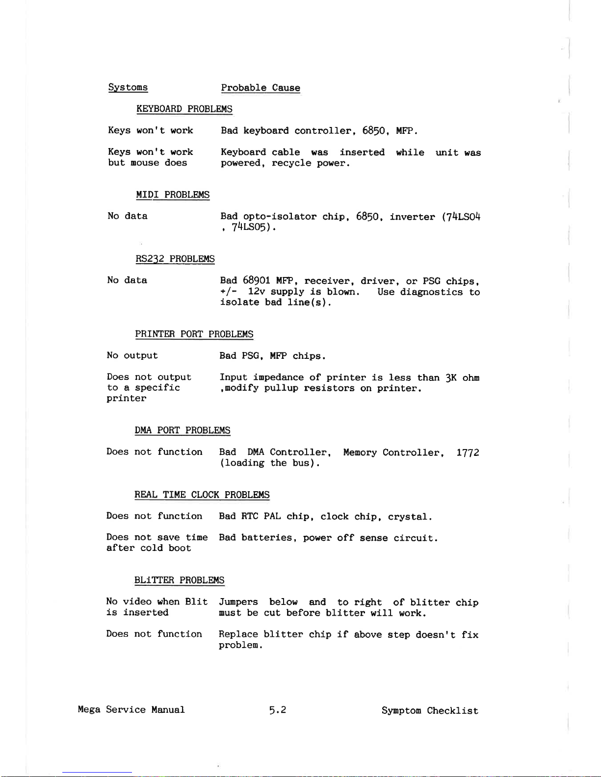
Systons
Probable
Cause
KEYBOARD
PROBLEMS
Keys
won't
work Bad keyboard
controller, 6850,
MFP.
Keys won't
work Keyboard
cable was
inserted
white unÍt
was
but
nouse
does
powered,
recycle
power.
UIDI PROBLEIUS
No
data Bad
opto-isolator
chip, 6850, inverter
(74LS04
, 74LS05).
RS232
PROBLEMS
No
data Bad
68901 MFP,
receiver,
driver,
or
PSG
chips,
+/-
12v
supply
is
blown.
Use diagnostics
to
lsolate
bad line(s).
PRII.ITER
PORT
PROBLE}IS
No
output
Bad
PSG,
MFP
chips.
Does
not
output Input inpedance
of
printer
is less
than
lK
ohn
to
a specific
,nodify
pullup
resistors
on
printer.
printer
DMA PORT
PROBLEMS
Does
not
function
Bad DMA Controller,
Menory
Controller,
L772
(loading
the bus).
REAL
TIME
CLOCK PROBLEMS
Does
not
function Bad
RTC PAL
chip,
clock
chip, crystal.
Does not
save tine Bad batteries,
power
off
sense circuit.
after cold
boot
BLiTTER
PROBLEMS
No
vídeo
when Blit
Junpers
below
a¡rd
to
right
of blitter
chip
is inserted
nust
be cut before
blitter
will work.
Does
not functÍon
Replace
blitter
chip
if
above step
doesn't fix
problen.
Mega
Service Manual
5.2
Synptom Checklist
Page 55

SECTION
SIX
DIAGNOSTIC
FLOII¡CHARTS
This
sectÍon
sumnarizes
in
diagra.natic
forn
the
steps
taken
in
troubleshooting
the
Mega
using
the
diagnostic
cartridge'
The
details
of
using
the
cartridge
are
not sho$m;
this
shows
the
context
in which
the
cartridge
would
be
used,
including
sone
problems
for which
the
cartridge
would
not be
useful.
Usage
of
the
ôartridge
is covered
in the
troubleshooting
guÍde.
In
general, the
user
would
run
all
the tests,
look up
errors
in
the
troubleshooting
guide,
and
take
the
action
reconnended.
Atthough
a
thorough
understanding
of
the
syste¡n
may
be
necessary
in solving
sone
problens, in
most cases
following
the
flowchari,
reading
the
docunentatíon
on
the
diagnostic
cartridge
where
necessary,
and swapping
out
the
indicated
conponents
will
result
in repair
of
the
Problem.
Replacement
Procedures
where
replacenent
is
indicated,
replace
the
conponent
(if
more than
one
is
indicated,
replace
one
at a
time)
with
a
kno*n
good
part.
If
other
components
are
later
replaced,
verify
whether
the
first
part
is
good
by
replacing
in
the
systen
once
the
system
has been
rePaired.
Handting
of
Integrated
Circuits
Extreme
care
should
be
taken
when
handling
the
integrated
circuit
chips.
They are
very
sensitive
to static
electricity
and
can
easily
be
damaged
by
careless
har¡dling.
Keep chips
in their
plastic
carriers
or
on
conductive
foan
when
not
in use.
Mega
Service
Manual
6.t
Diagnostic
Flowcharts
Page 56

START
CONT\ECT
TERM¡NAL
TO RSæ2
PORT
CYCN-E POWER
IS DISPI.AY
RE.ADABLE
?
DISPLAY
ON
TEFINô.¡AL
?
REPLACE
PARTS
PER
DIAGNOSTIC
GI,JDE
RI.}.¡
ALL
TESTS
DAGNOSTIC
ERROR?
FEPLACE
PARTS
PER
DIAGNOSTIC
GUIDE
CYCLE POWER
OTHER?
MEGA/ST DIAGNOSTIIC
FLOtll
CHART
Mega
Service Manual
6.2
Diagnostic
Flowcharts
Page 57

NO ERROR ON
DAGNOSTIC
RUN DISK
DAGNOSTIC
OR
REPLACE
DRIVE
TRACE
SIGNAL
FROÌ\, VDEO
SHFTER
TO
OTJÏPUT
RUN
APPROPRIATE
TEST
CONTINUOUSLY
MEGA/ST
DTAGNoSTTTC
FLoW CHART
PROBLEM
FOLAD
?
CON¡TACT
ATARI
TECHNICAL
SUPPORT
Mega
Service
6.3
Diagnostic
Flowcharts
Page 58

NIO
DISPLAY
ON
ìvlOÀtTOR
OR
TEruINAL
\
t/t/
t€
TN
\'
1. CI€q<
SHIFTER
2. REPLACE
OSCILLATOR
FEIVIOVE
SHIELD
NSPECT
PCB
TEST FOR
SI-{OFITED
+
5
V
FEPLACE
POWER
SUPPLY
t€
FEPLACE
GLUE
FIEPLACE:
1. GLUE
2. ltlBMORY
CONTROL
3.
CPU
YES
l€
REPLACE
PCB
FEIVIOVE
Sl-lORT,
RE€HECK
Fts232
DISPLAY
?
DAC¡l'.lOSTlC
1.
SEE
THEORY
OF OPERATIO¡¡
2 REPLACE
PCB
3.
COf..¡TACT
ATARI
.IECHNICAL
SUPPORT
REPLACE
PARTS
PER
DIAGNOSTIC
GUIDE
6.4
Mega
Service
Ma¡rual
Diagnostic
Flowcharts
Page 59

NO
DISPI.AY,
Ì\¡O
ERROR
REPLACE
XTAL
RESTART
MEGA/ST
DrAGNoSTrrc
FLow
CHART
RESTART
32
¡úHZ
cLoo< ?
REPLACE
SHFTER
OTJTPUT
FROM
SI-IFTER
TRACE
OUTPUT
TO COI\¡€CTOR
FìEPLACE
FAT-}G
PART
REPLACE
tì/EMORY
CONTROLLER
RESTART
Mega Service
Manual
6.5
Diagnostic
Flowcharts
Page 60

Page 61

SECTION
SEVEN
PARTS
LISTS
AND
ASSEMBLY
DRAWINGS
Mega service
Manual
7.I
Parts
List
&
Drawings
Page 62

PART
NUMBER
cA200055-00
1
cA200093-001
cA200008-001
cA200018-001
cA200022-001
cA200025-00L
cA200039-001
cAz00040-001
cA200041-00L
cA200042-001
cA200043-001
cA200054-00L
c070350-003
c070352-003
clû3047-001
cAo70025
MEGA PARTS
LIST
DESCRIPTION
PCBA
(l¡le
no¡¿)
MEGA
4
PcBA
(1Me
no¡¿) MEGA
2
MEGA
POWER SUPPLY
w/FAN
MEGA 2/
4
CASE
BOTTOM
MEGA
2 CASE
TOP
MEGA
4 CASE
TOP
MEGA KEYBOARD
COMPLEÎE
MEGA
KEYBOARD CASE
TOP
MEGA KEYBOARD
CASE
BOTTOM
MEGA KEYBOARD
CONNECTOR
PCBA
MEGA
KEYBoARD
(on¡r,y)
MEGA
KEYBOARD CABLE
FDD
uNrr
(1v
eyre)
r,¡nwrRoNrcs
FDD uNrr
(r¡4
gyre)
cHrwor.¡
FDD uNrr
(ru
ayrn)
cHrNo¡¡
STM1
MOUSE
ASSEMBLY
cAP
30pF 50v
+5% cH.
cER
AXIAL
CAP 39pF
50V t5%
cH. cER
AXIAL
cAP
100pF 50V
t5% SL.
cER AXIAL
CAP 150pF
50v t5%
cH. cER
AxrAL
cAP
330pF 50v
tl-Oå B.
cER
AXIAL
cAP
1000pF
25v
+202
x. cER
AXIAL
cAP 0.1pF
25v2.
cER AXIAL
cAP
O.221tE
50v z5U.
cER AXIAL
CAP 0.47¡:F
25v z.cER
AXIAL
cAP
4.7pF 25V ELEC
AXIAL
cAP
10pF
16V ELEC
AXIAL
cAP 47ytF
16V ELEC
RADIAL
cAP
100pF 16V
ELEC
AXIAL
cAP
1000pF
L6v
ELEC AXIAL
cAP
4700¡rF L6v
ELEC
RjADIAL
cAP
L00L¡rF
16v ELEC
RADIAL
cAP
5-30pF TRIMMER
RES O OHM
JUMPER
5.1
oHM L/AW 5%
CARBON
27 OHM
T/4W 5% CARBON
33
OHM L/AW
5å CARBON
RES
47 OHM
L/4W 5å CARBON
RES
75 OHM L/AW
5% CARBON
RES
1OO OHM L/4W
5% CARBON
RES
].50 OHM
L/AW 5%
CARBON
RES 220
OHM L/AW 5%
CARBON
RES
470 OHM
I/AW 5% CARBON
RES
].K OHM T/AW
5% CARBON
RES 1.2K
OHM L/4W
59" CARBON
LOCATTON
SUBASSEMBLY
SUBASSEMBLY
SUBASSEMBLY
SUBASSEMBLY
SUBASSEMBLY
SUBASSEMBLY
SUBASSEMBLY
SUBASSEMBLY
SUBASSEMBLY
SUBASSEMBLY
SUBASSEMBLY
SUBASSEMBLY
SUBASSEMBLY
SUB
FOR
ABOVE
SUB
FOR
ABOVE
ASSEMBLY
c39,40
c54
c43-46
c28
c29
c68,69
cL,2,5-7
,9-2L,23,26
27
,30-33,36,38,4t,
42
,47,49,50
,52 ,55 ,
56,57, s9,60
,64-66 ,
70
,73,LL2,113
,t20
,
L2L-L23
c80-95
c67
c22
,
24
,25
c3
c34,35
c8
,
37
,51
cL40
c4
c49
c53
Rl20
,L23,L26,L45,
146,DL2-L4,w2,3
Rl5
R83
R52
,54
,55 ,57 ,60-66
68,76,110,l_13
R45-48
R67,73
,77
R69 , 75
,78,
86 , 116
R23,115
Rl0
,
L4
,L6 ,17 ,Lg ,44
R26
Rl,2
,4,2t,24,30
,37
38,40-43,82,85,111_
R20,76
RES
RES
RES
Page 63

PART NUMBER
c070567-004
c070 1 59
-00
6
c070
448
c014384
c070205
c070471
-001
c07047L-002
c0?0790
c07024L-002
cl01805
c025993
cll0232
c1 00281
c010L29
c070130
c070131
c070134
c070033
c070445
c070644-0 L
1
c10028
3
-00
1
c070120
c070119
cAO70024
cAo70023-003
cA200053 -002
c]_01_643
c025982
c025913
c025915
c0259L4
cl0 160 I
c0259L2
c025986
c025981
c025983
c025984
c025985
cr0L7t2
c025988
DESCRIPTION
RES
2.2R
OHM
]. / 4W
52 CARBON
RES
3.3K
OHM
]. / 4W
5% CARBON
RES
4.'7K
OHM
1. / 4W
5Z CARBON
RES
5.1K
OHM 1/4W
5Z
CARBON
RES
lOK
OHM L/AW
5% CARBON
RES
12K
OHM L/4W
5% CARBON
RES
51.K
OHM
T/ 4W 5å CARBON
RES
NET!{ORK
lK OHM X
6
RES NETWORK
4.7K OHM
X 8
RES
NETWORK
lOK
OHM
X 8
INDUCTOR
FERITE
BEAD
AXTAL
INDUCTOR
O.27UA
20% AXIAL
INDUCTOR
L0pH
10% AXIAL
INDUCTOR
220¡tH
L0% AXIAL
LINE FILTER
NOISE
FILTER ZJS5lOL_02
TRANSISTOR
2N3904
TRANSISTOR
2N3906
DIODE
1.N9].4
DTODE
].SS1O8
SCHOTTKY
BARRIER
CRYSTAL
2.4576
MHZ
CRYSTAL
32.768RH2
CRYSTAL
32.0424
MHZ
CONN
40 PTN
RIGHT ANGLE
CONN DB-19S
HARD
DISK
CONN
L4 PTN
DTN
FLOPPY DISK
CONN
DB-25P
RS232C
CONN DB-25S
PARALELL
CONN 13
PTN DIN
VIDEO
CONN
5 PIN
DIN MIDI
CONN
SINGLE INLINE
6 PIN
CONN
DOUBLE INLINE
24
PIN
CONN
DOUBLE
INLINE MALE
64
PTN
SOCKET
40 PIN
SOCKET 28
PIN
SOCKET
68 PIN
LCC
PUSH
SWITCH
FLAT
CABLE
34P ASSEMBLED
CABLE
4P ASSEMBLED
CABLE
ASSY:MALE
TYPE 2 PIN
IC
CUSTOM
ST
BLITTER
rc
68000-8
cPU
IC
CUSTOM DMA
CONTROLLER
IC CUSTOM
GLUE
IC
CUSTOM SHIFTER
IC CUSTOM
FULL
SHTFTER
(W/D/A)
TC
CUSTOM
MMU
IC 1489
RS-232C,
RECEIVER
IC 1488
RS_232C,
DRIVER
fC
YT42L49
,
SOUND
IC 68901,
MFP
IC
6850,
ACIA
IC
DYNAMIC
RAM
1M X 1
IC
PC9OO
PHOTO
COUPLER
LOCATION
R5
R27
R6,1L,28
,29
,39
,LLz
R22
R7
,8
,25 ,33-36
,
108
,
L09,114
R18
R32
Ro7
nþr
-q
RP5
,6
LL
,L2 ,45 ,46
,48
L47
L50
L5
L9
L2-
4
,6-8 ,L3-22 ,24
-30,32-43
Q1,3,6-10
Q2
D1-3,5-8,15-18
D4
Y1
Y2
oscl
J2
Jl0
J13
J7
J6
Jl4
J3
,4
Jl,18
JL7
J15
v27
,3L
u3,4
,6 ,7 ,9,10
u5, 17,30
S1
JL2
Jl1
J9
U5
U8
v27
u17
U31
or
u31
u30
ul9
v20
u16
u18
u],4,15
u40-55
(
60-7s
)
u13
Page 64

PART
NUMBER
cL0L62t
cL0L622
c101.625
co1044'l
c026028
c10
1629-00 1
c101
630
-00
L
c070349-002
cl00296-00
L
c070322
c070323
DESCRIPTION
rc rL
7705A
rc 74Ls02,
QUAD
NOR
IC
74LSO6,
HEX INVERTER O.C.
IC 74LSO7,
HEX
O.C.
BUFFER'
rc 74Ls32,
QUAD
2-TNPUT OR GATE
IC 74LS]-48
8-3 PRIOR ENCODER
rc 74Hc00
guAD
NAND GATE
IC RP5C15
REAL TI¡,IE CLOCK
IC
RTCPAL PAL16L8
TC 74L5244.3 STATE LINE BUFFER
TC 74LS373 LATCH
IC 74LS].].
TRIPLE 3-INPUT AND GATE
IC TL497A
SVIITCHING REGULATOR
TC WD-L772
FDD CONTROLLER
IC;
TOS ROM 1 MEG HI-O
IC; TOS
ROM 1 MEG LO-O
AC POVTER CORD
(Ur,zCSe)
MEGA MANUAL OWNERS
COLLAR
A
COLLAR
B
LOCATTON
ul.
U2L
v26
U2
u78
u39
v24
u25
u37
v32
,35 ,58 ,59
u33
,36
vL2
tJ22
v28
U9
u10
3 DRIVE SPACERS
1 DRIVE SPACER
Page 65

G)-
Ql,^
:o
I ATAnl ÍJAPAiN COßPORÂNOT¡
,/l\ t-"..-;
x'vor¡, Bu'd,m s
filfiPl'
a-:ro
rdamffi
M'nâbku.
rdp t6
r4A//,/
ASSY
l4EGA
Stur:
D*rst\r.
\rt
-
iÍr
c
_)c
! \t¡
NONE
srtd
3
0t
3
Page 66

i\
I
c
I
I
I
I
I
?;
OO
æ
I'f
I ATAF
(JAPA¡{I
OMONAT(T¡
a4\.-
t-*
K'yd'
Bú6q
lffif,l'
r-r-ro raatm
M,rb¡o róþ
p5
PCB AJJY
NE6A
slzf, D¡^*lIr:
\o
¡tt
(A
\\t¿
NO^/ê
:ren
¿f
,*
I
Page 67

t
A1
¡lJ F¡x)cæon
tfpr
/l\- r-*
xd
ffi t
ATAII-
++r. ro.*
*¡oiu. rcp
o
Page 68

w
I
\_]
cAo.totôt¿ç
-
xxx
Ar
E
(Jamr0
oo¡Fq^ü)x
fd@
X'Fû
tubq
lF
+3-þ
lq!ffi
Urñtu
t*F
t6
HA|N
ASSr
.Jrrr I
{tE
-ri¡aaiir.,
ä'
iir
C.
_
E
*
\t
tyONE
crrB
S
ú
J
Page 69

SECTION EIGHT
SCHEMATICS AND SILKSCREEN
Mega
Service
Manual 8.1 Schenatics &
Silkscreens
Page 70

Page 71

A
ií
pnooucrtoNRELEAsE
J'
HAIN
,---5
IINê.
FILIER
¿í
J1
KEY&URÐ
J2
JOY
'
-t
s
T
xÐATA
RxÐlTA
+.1v
xê./uP
,t.
¿aUrfOP/tlRE
8U77dtV
r-1
c:--3'(
XA,/ÐowN
YA/¿EEFî
YE/RlEHT
UP
R BurroN./FtRE
Burrav
N-.a-ì
F
ÐowN
¿EFT
RIEHT
KEY
ENÐ
ÐETAIL I
J3
JOY
I
TOLERANCES
)RAIYN
8Y DAI€
I
t-tJ
o-/.H
I
ATAfl(JAPAN)OORFOR^rþil
/N.
Torônomon Klyo3h¡
Bulldlng
3F
ATARI-
+$t0, Toranomon Mtn¡rcku,
Tokyo lo5
UNDER
30
+0.1
:HECI(ÉO OATE
c ¿'L-- h.27-l
30
rHRU
300
!o.2
NONE
FILTER:
SfA DETAIL
'
NOTES_UN
LESS
OTHERWISE SPECIFIED:
ovER
300
+
0.,0
:NGINEEf, OAT€
â.91¡æc¿2"æt
""WlEÌrArtc
olAe?AH
J¿¿B
Æg
¡.¡tAA f Ptràrt.a.Ptt \
^)-/
l2-ro<
Æ43.-
(
kÈYà.rapt^')
IPPflOYED
OATE
s,ûl¿llt
.Liltc
srzE
loR
rYr.{o
ilo
REY
A
NEXT ASSY usEo oi¡
Ê¡¡r'sx
-
rytïø.
/;ï,
sc^rt
NONE
lsnesr
I
æl
APPLICATION
Page 72

vcc
ul ¿3at vt
ì!îÞs\ñ4¡baÀ
\ \t È \ \ \ \ \ \ \ \
/ottz
,
ð
a2NNECfO/<
r./-'nols¿
r/Lr¿R
,/t Ò lE
s
-
u
lt¿
E s,:
oaHERrø
:E,5?E
a/F/ E
t
¡!r lñrri¡
lrt-r
¡ll't¡¡¡
PROOUCTION
RELEASE
A2æo€lxv
t
ar
E
(JAHfl)
coRFoR
Tþil
/f\-
t."*
x,yd¡
Build,ù
ATARI-
.-J-'o
rsa.m
u,o¡o-l¡o
r*yo
ros
4E8,+
_
(kt-recAkþ)
stzl:
0t¡tt\ti
\0
/o
ttt
A
s\^tr
tuail¿:
\xÊlr
t
.f
.
Page 73

pFt
slitrtil
c?r
o.ØzL
)Í=
0"
8uço8
tt
r1
I
lt
lr
¿
?
/N139t
âlt
ttov
roov
ìr?v
3P
/N¿ET
clltss/s
ONo
R8
tt2
ll
lt
ll
ll
ll
t3
.ç
Rt8
é8ß
2V
rsy'
OV
TYPICAL
IC3
T
o.oltF
L
¿çov
RI?
J.3r4
Cr/
O.?2sF
lov
C¡O
:
Qo?zrF
tov
f
tot¡t
H
t/2v
¿ton
PJ
2V
,îoXn
t/2v
,"5
,n
?w
R,¿
??o
n
t/2v
LI
Rø
t?on
@3
74Nt
(TI)
t70n
rl:v
A
Bf
YlsÍr\s
tr!:.1('tll'ltol
PRODUCTION RELEASE
I St:l) 0l
ASP34
-/
I
ral;/-
1/11n
H1;(
lil:tl t)¡Tt:
t.àçt 9-Ê-Sl
;irr:fH
-'
-'l-ntî
4.1w-:y
^
ATARI" ro5
Page 74

AC
AC o-
I
I
I
I
il
c9
0"
auîoa
r,/
|
"2
/tOv
it':
ct2
22Ôo/'F
25v
tt?v
/s'_,
J,.¿..
¡5V
OV
R8
ft2
lr
ll
tl
.'a
TYPICAL
5'll'ç
Ðz
loorFl
¿ç{
5.3obr
¿çov
I
o.?2:F
lOV
,t"'
t'
'.tKt
+
/5Ot\0,
R¿ ¿
t/zw
JJor¿l
2
,eJ
?
//
,îOt<fL
,
/2v,/
esoTr
zîV
Rt,
,?o9.
Rro
t?on
o3
7¿aJt
(TI)
CtO
;lt::,^
5ov
Rt3
t.'"-
|
I
,"
'R/4:
5.tKt
770tL
\t:
,',J['
-:
l)ta \tr
\
til
l) \¡l:
i,Ler.ltL-
4/a/".
elt tt h ¡:t)
l) rlt:
.s
-'-'?-::¡='-t2-8-?
t:\r,¡\l:!:R DrTl:
1...4!¡"ç¿:g_4rt_4
N
ATARI
(JAPAN)
CORFORATION
./l\.
Toranomon
K¡yosnr
aurrd¡ng JF
ATARI
4-3-rO,
Toranomon tv¡rnato-ku
Tokyo
,tos
TOLERANCEI
t:\ t rs{ì
"'"'
scHEHAnc
Ð/AGRAH
/À,1Þ ta- ì \
UNDER
3ll
=o.t
30 Tr-jFU 3001
-
0.2
ll \lERt \;.
rtlt
trK \lt l\rr
\r)
REv
B
HARD DRIVE
A
t-t\tsfi
=/
lue
3oo
i:0.¿
*:,ïi:'
'i.ï,
i(
\r.r:
/VO.VE
|
iltr:Fl
,/t
ir
I
Page 75

lA
Ðt
x8
Ð2
Y6
YA
3
ICt:/PCas98
oR
TA?5339F oR
EQU|VALENT
2
at- Q4
|
nþro 7e4tv's/s70î
L7R30t
oR
EOU|UALENT.
/ D,
-Ð4
|
LED
LfE
-sof
OR EOU0/ALENT.
NO|ES
-
¿/^/¿€ss
oTHERwtsE
SPECtFtEÐ:
6NO
-
\
\s.
À'
ù:
Y
LEFT
SW
9.-6
^ïDItf
r
STM
Í
s tìrT
Assl
/-
-s-
ÍATI:Rt¡-
ISH
--/
SCHE
I"'ATI
C
DIAORAM
Q'OASE
Bi
-
i¡
i
s( \t.t:,
lvto^tE
;
sur:nr
t
¡t
/
Page 76

Page 77

nÉv¡5ro¡s
utv,lrtltd
SEE SHEET
1
I
I
--ä-
å
=fl-l
-
:-..(i
ilË,ilrfrffi
o,Ëi
m"'
I'T
.Jq
:5-l
tt:,
t
EÌ:¡!
FI
01
J/LK
PR/NT
utr uaa
sr.-G'ü
*O...
ut¡
O
crd
[r
=.r
)l
út¡Oarú
-Oa*
)r
--
arot
clr
utr 6r
uroOcroa
øOcù
d
o
cro
*a
Éaa,
s-crß
øO.-
F?
-
car
u¡
,---
---
J
ô
/-
NOTES_UNLESS
OTHERWISE
SPECIFIEO
I AIAF 0rp¡l¡l @nPonarþr¡
/'l\-
to,.--on
*,roshr Bu,ro,^s
AIARI
.
3
to, Tor.nollM
Mrn¡to
¡o.
Tolto 105
^mvao
o^rÊ
.\"/já./
_./,
/
30THRU
æO
I
tO2
srÉ
lm^wilG
¡o
nÉv
cl
A
*tL¿
¡r'
O
NE
I
s*er
I
ot
(
Page 78

¡fv
I
n¿vrgùË
Oas¡rfr&
Bfa
¡p.aoJro
CONPOflEilT
J/ÐE
I'
.l
SE
'ï
9
íì
CED
O
ooooocr)
O
OO:CD
0
9,,
oa)
oo
T-,.'-
8
o
tr"
4çqoccro^
oooo:.tc ooocoooo
cccocoo! ocoocooó
./
E-.-EFìoa
occ ac
go
cr.i'-Y-"-rE+moooo
oooqocÐ ococ5oco
oSoooooo
O
*<¡¡rt¡5ùoocooooo
NOTES-UNLESS OIHERWISE SPECIFIED
UNDER30
|
tOr
30rHRU3æl
to2
oven¡m-Ttrii
I
ar n(JlP^il)oonPonar0¡
/'l\-
to-.o.on *,yoih¡
Bu¡rd,.o
ATAflI'
.J
to. Io.Momoñu'¡¡ro¡ú
to¡ro roâ
PCð
NE6A
sr¿E
lDbwrs
rc ¡tv
cl A
*¡t¿
NO
/y'E i sx.rr
\l
or
ã
Page 79

\tô/_ÐER
i/ÐE
NOIES_UNLESS
OTHERWISE
SPECIFIED
ovER3{Ð lto¿
t¡'-,"
/./¿'
I
AIAfl
(JAPA¡II
OORFOAAT¡O'¡
.4\
ro.¡nomon x''osñ,
Bu',o,ñq
llfifll'
r
: ro. ro'r"omoñ M¡ñ¿ro åu Torro
ro5
PcE
nE6A
sr¿É
ioF^w'ñG
ño ¡Év
ci
A
s^t.
NO//
ê
I
s*tr ( or
¿!
Page 80

..ttttttitt
O
. .
-aaaaa
r:::::i:':¡::
'..o:':
;-.;ilbE..'"
i....
t
ffi
'
..
.
..
.
i?:''f
.*iÏ..?I;."""":"":::":'.=.?::::::..::i:'
-..
'.
¡u
.
'..-1.
:.j.....:....
t
t
-t!"""1
t
'
.
t .......
t
.
t.^..
a
"""'
¡-
.
aa
a a
r.
i
..t
.t
-.'
.:.1.¡.......
..........
.
.......a
o'¡.t
.
t.....t.ta......
......
t;:
:,;"
.'.i.'i-.'-;.:i
.-';;"'ïil;:':
il:
:i::'i'',i
.
l:ïi:::l;:t:
-
-
^.^:
: ::. tt-
.','-'-'1""""""ìi''3:3:333333:3:t:a'''.:l
.p¡:':iii
;r'.'.'..*:::::::::j.;ii::'ö:::::;lii::::;:i:.
.::::::;:::.:.....i...
:3....:..:..
. . !¡¡¡¡.-..-
,.
.J.
.-.:.
.....-...-
.....;...-
.
.....;...
.........
I
]
I
-....¡....
3r.........
.
'.....3....
3¡........
.
i:::::t:::^
i
:
l,
îï1¡.:i'f¡i:::.
.:::::.;:::.
':::::;:::
f:i':=t'=i+ii'--,.-¡i
.,:
Ïii'',¡ei
:
:''
Ï::::T::'ï::::i
::ii::::
:îÏ:;:ii'
i!ii:
-':-':ïï'1
'
'."'.t!.
l.
r"'..O;
..
.
: .
.I
e
!'
'eoo'1._^':l
JOLÐER
NA''K
ConpoNEilr
s/.ÐE
NOIES
_UNLESS
OIHERW¡SE
SPECIFIED
¡av
iavr!@3 &*n¡Ptù
ùra
^pruvto
30THRU3an,
!02
I
AT fl(J
PA¡it)COnFlOf,^I(It
/f\-
ro,.no.on
x,rosh¡
surd'oq
ATARI-
¡.¡ to ror¡nmn
r,n.ro ¡u ro¡yo ro5
¡tta
PCå
NE6A
*r
Imnxcrc
,
ruv
çl
A
w*
2¡¿
¡¡
f
l,
stet
,f
oc
ó
Page 81

Ac
/n(H
)
FASE
PCð,4SSr
AC
/At
(ty)
POWER,'OCKET
co70E/5
-
æ
/
FAN
c/oo
2/5 -
o/t
FRAP'E
G^tÐ
POWER
'îOCKET
(/?EAR
V/EW
)
oü
[[Ho
POWEI?
JWITCH
(
/?EAR
VIEW
)
rsv
6NÒ
t
t2v
CONNECTOR
fOROtÐ
CORE
wtt"tMç_
3 TURNS
POWER
.lWlrCH
coToëtó
t2
ITE
ûARO/Ð
CORE
co70922
i
FRANE
6NÐ
REv
i
REV|S|ONS
DESCR|PI|ON
DAIE APPROVEO
SEE
SHEET
1'
It.F"w¿l^2-4'67
CHECKEO
OAIE
A,
l-7t*r
-
-?o
3i'
ENGIN€Eß DATE
À',)rna4tt
'4,"¡ry
\PPROVED OATÈ
T
ATAR¡
(JAPAN)
@RPORATION
.4\.
Toranomon Kryoshr
Burtdrng
ATARI
4.3.10. Toranomon Mrnato-ku.
Tokyo
105
POWER
\taPPLr
zf
.JJ
X
ASPJ4-t <//7Y)
SIZE DRAWING NO
,
REV
B.
I
scete
)¡Q)/f
snÊEr
5
or
ó
NOTES-
UNLESS
OTHERWISE
SPECIFIED:
AîT
}4
rHrÂOANGIE
SYSlEr
OrúEtS|ON ññ
Page 82

OETAIL
A-A
.-=\
':**
a,'1
e
{9
\
-e.Fl
d .-eS
e
:=2'
Page 83

þof¿s.
(uþL¡sí
07t5nwtsÈ
sPEctFt40)
t
^LL
zesttfogs
^ac
ME^3VÞEE .u
olqtt
'/-w.
s* -
2
ALL
'AA¿I|OR!
AzE /4EA'UCEO
IU
P'¿O
FAPAC6,
t
-aatlpÂL
aouþf
ts
^<rtv€
auPtuô TPE LAsf
TPANaFfe-
9 aAA
sttÍE: þotl
7O Åê4,
¿4A
REAÞ.
ñfH
lÒ 1oa,.
at
, t<
XD<S,H
L6CpO
L^57
pUHaæ
USfO:
il
wPtf¿
-
L
r
atuS
NNe
,
ic,ú.L
ÞEA ,ZaaD
f.NTR¿O L
L^'r
Da.aaapca
oBtlþafoP
',u
z'
'
k7
'_a
z
ra-¿
I
I :tl
I
e¿ìieiä¿ Lisøptr"às
*-r
l"- ¿ ri
,¡q
utêè
u*a
----Ã
-Èå!-
Page 84

Page 85

Í,
):
I
ð
t
I
2
I-
l r.-
L::t .
ts.
|
-.-
r-
--
I
1_
I s¡Á
1..
i
I
t5
;-
--tr
el
r--
l"'-
úla
i
ø ø
Ul
f'
t¿Ltoo
14 LtOA
JÒtsrlcÉ aþd
pptp|Ep
râ7
FtxT
Page 86

Page 87

SECTION NINE
GLOSSARY
OF PART
NAMES
AND TERMS
BITBLiT--Atari
graphic
chip which is
actually
a
DMA
device.
It is
used to tra¡rsfer
block
of
memory
from
a source to destination
with
the
patterns
and
a combination
of any
logical
operations
between
source
and destination
which
was set up
prior
to the
transfer.
BUS
ERROR--GIue
has
asserted BERR
to
inforn
the
processor
that
there
is
a
problem
with
the
current cycle. This
could be due
to
a device not responding
(for
exa.nple, CPU
tries
to
read
memory
but the Menory
Controller fails
to assert DTACK),
op
an illegal
access
(attenpting
to write
to
ROM).
A bus
error
causes
exception
processing.
CPU--the
68000 microprocessor.
DMA--direct
¡nenory
access. Process in
which
data
is
tra¡rsferred
from
external
storage device to RAM,
or
from RAM
to external
storage. Transfer is
very fast,
takes
place
independent
of
the CPU,
so the CPU
can be
processing
while DMA
is
taking
place.
Glue
arbitrates the
bus between the
CPU ar¡d DMA.
DMA
CONTROLLER--Atari
proprietary
chip which
controls
the
DMA
process.
All
disk I/0
goes
through
this device.
EXCEFIION--a
state
in
which the
processor
stops the
curent
activity, saves what it will
need
to
resune
the
acbivity
later in RAM, fetches
a vector
(address)
from RAIft,
and starts
executing at the address
vector. When
the exception
processing
is
done, the
processor
will
continue what
it was
doing
before the exception
occurred.
Exceptíons
can be caused
by intemupts, instructions,
or
emor conditions.
See also
Section Two,
Systen
Errors,
or a 68000 reference for nore
detail.
GLUE--Atari
proprietary
chip which
ties together
aII system
timing and control signals.
HALT--state
j-n
which the CPU is idle,
all bus
lines
are in the
high-inpedence state,
and can only
be ended with
a
RESET
input.
This
is
a bi-directional
pin
on
the CPU.
It
is
driven
externally
by
the
RESEtr
circuit
on
power-up
or a
reset
button
closure, and
internally
when
a double
bus
fault
occurs. A
double bus fault is
an error during
a sequence
which
is run
to
handle
a
prevíous
error. For
sxamplê, if
a bus emor
occurs, and during the
exception
processing
for
the bus
error, another
bus
error
occurs,
then the CPU will
assert
HALT.
Mega
Service Manual
9,1
Glossary
Page 88

HSYNC--timing
signal
for the
video
display.
Deternines
when
the
horizontal
ðcan
is on
the
screen,
and
when
it
is blank
iretraci.ns).
The
synchronization
(approx'
every
63
microseconds)
also
is
encoded
onto
IPL1,2
as an
interrupt
to
the
CPU.
II,ITERRUPT--a
request
by a
device
for
the
processor
to
stop
h¡hat
it
is doing
a¡rd
perforn
processing for
the device.
It is a
type
of
exception.
Interrupts
are
naskable
in software,
neaning
they
will
be
ignored
if they
do
not
meet the
current
priority
tevèl of
the
CPU.
There
are
three
priorities: the
highest
are
MFP
interrupts,
then
VSYNC
interrupts'
and
lowest
are
HSYNC
interrupts.
Interrupts
are
signaled
to
the
cPU
on
the
Interrupt
Priority
Level
inputs
(IPL0-2).
see
Theory
of
Operation,
Main System,
MFP,
and
Glue.
MEMORY
CONTROLLER--Atari
proprietary
chfp
which
ha¡rdles
all
RAM
accesses.
see
Theory
of operation,
Main
systen
a¡¡d
video
Subsysten
for
details.
MIDI--Musical
Instrunent
Dígital
Interface.
An electrical
standard
by
which
electronic
instrunents
comnunicate.
AIso,
the
lógical
sysgen
for
such
comnunication.
In
the
1040ST,
consists
of a
6B50
connunications
chip,
driver
and
receiver
chips
(74LS04,
74LSO5,
and
PC-900
photocoupler),
and
an
MFP
interrupt
channel.
MFP--MuIti-function
Peripheral,
atso
68901.
Interrupt
control,
timers,
and
usART
for
RS232
connunicatÍon.
see
Theory
of
Operation,
Main
System.
MODULATOR--device
which
combines
video signals
R,G,B'
VSYNC,
and
HSYNC
into
a
conposite
s:'.gnal
for
nonitors
requiring
this
typeinput,andalsomodulatesthissignal,combinedwith
audio,
onto
a¡r
RF camier
for
output
to
a
television.
PHASE
LOCKED
LQOP--circuit
which
locks
the
horizontal
sync
signal
onto
the
color
burst
reference
frequency
for accurate
color
on
the
T.V.
lrJithout
this
circuit,
colors
on the
T.V.
become
unstable,
flickeríng
or shiftÍng
about
on
the
screen.
The
PPL
may
be
on
a daughter
board
located
in
front
of
the
video
shield
or
hand
wired
onto
the
naÍn board
within
the
video
shield,
or
(possibly) in later
versions,
integrated
into
the
printed
circuit
board.
PSG--Progranmable
Sound
Generator,
also
YM2149.
Yanaha
version
of
Genéral
Instn¡ments
AY-3-8910.
Has two I
Uit
I/0
ports and
three
sound
channels.
used
in
parallel
port
and
audio.
Rs232c--Electical
standard
for serial
digital
comnunication.
AIso
the
physical
and
logical
device
which
perforns
comnunication
using
this
standarã.
In the
ST
computers,
consists
of
the
MFP,
PSG,
1488,
and
1489 cniPs.
Mega Service
Manual
9.2
Glossary
Page 89

L772--Western
Digital
Fl-oppy
Disk
Controller.
6850--atso
AcrA
(Asynchronous
connunication
rnterface
Adapter).
rnterfaces
between
B
bit
pararlel
bus
and
serial
communication
bus.
In
the
ST,
there
are thro
6850s,
one for
keyboard
conmunication,
and
one for
MIDI
conmunication.
6890t--see
MFP.
SUPERVTSOR
MoDE--state
of
the cPU
in
which it is
arlowed
to
access
alr
hardware
a¡rd RAM locations,
and
perform
sone
priviriged
instructions.
Deternined
by the
state
of a bit in
the
status
Register.
The
operating
system
operates
in
supervisor
node,
and
switches
to
user mode
before
passing
control
to
an
apprication
(although
the
application
ca¡r
enter
supervisor
mode
if
it
wishes).
usER
MoDE--state
of
the cPU in
which
certain instructions
a¡rd
areas
in
the memory
nap
are
disallowed
(resulting
in
a
privilege
violatÍon
exception
if
attempted).
See
also
SUPERVISOR
MODE.
vsYNC--signal
used for
vertical
synchronization
of cRT
display
device.
Occurs
aE
70
Hz
(monochrome),
or
50
or 60 Hz
color.
l¡M2149--see
PSG.
Mega
Service
Manual
9.3
Glossary
Page 90

 Loading...