

Page 1

Page 2

ATARI
ADVANCED
FIELD
VIDEO
MODEL
SERVICE
ENTERTAINMENT
5200TM
MANUAL
SYSTEM
Page 3

A
tari believes that the information described in this manual is accurate and reliable,
and much care has been taken in its preparation. However, no responsibility, financial
or otherwise, shall be accepted for any consequences arising out of the use of this
material.
to
advise of
Information
such
changes and/or additions.
contained
herein is subject
to
change. Revisions
may
be issued
.
Correspondence regarding this document should
be
forwarded to Director of Technical
Support, Consumer Product Service, Atari, Incorporated,
California
94086.
845
W.
Maude, Sunnyvale,
Page 4

TABLE
OF
CONTENTS
Section
Title
-
INTRODUCTION
OF
THEORY
Overview
Model
SILKSCREENS
4-PORT
5200
Four-Port Universal
Two-Port Universal PCB differences
Outer Case
RF
PC
Switchbox
Game Controller
OPERATION
Console
PCB
differences
Shield
Board
Microprocessor Chip
Alphanumeric Television Interface
Controller (ANTIC)
Graphic Television Interface Adaptor (GTIA)
Pot Keyboard Integrated Circuit
AND
SCHEMATICS
MODEL
5200
TESTING
-
MPU
Page
(POKEY)
-
CX5200
Field
Service Manual
Equipment Requirements
Testing with the Diagnostic
1
Cartridge (Version
Overview
Initialization
Power-up Screen
Solid
Vertically Lined Screen
Snowy Screen
Warped-Ragged Picture
Color
Gray
Any Video Screen
Pokey Adjust
Error
RAM
Verify
Port Test
Tone
of
Tests
(Black)
Bar
Test
Bar
Test
Summary
Test
ROM
Test
&
Colored Screen or
.l)
iii
Changed
ECN
/I0036
6/21
/83
by
Page 5

TABLE
OF
CONTENTS
(Continued)
Section
Title
-
2-PORT MODEL 5200 TESTING
Equipment Requirements
Testing with the Diagnostic Cartridge
(Version
Overview of Tests
Initialization
Power-Up Screen
4-PORT
1.1)
Solid Colored (Black) Screen or
Vertically Lined Screen
Snowy
War ped-Ragged Picture
Color Bar Te
Gray
Any Video Screen
Verify OS
Tone Test
POKEY (Port) Test
RAM Test
POKEY Adjust Test
POKEY Softfire Test
Screen
Bar
Test
ROM
5200
DIAGNOSTIC FLOWCHART
Overview
The Swapout Procedure
Replace in Order
ATARI Repair Hotline
2-PORT
4-PORT 5200 SYMPTOM CHECKLIST
2-PORT
GAME CONTROLLERS
Over view
5200
DIAGNOSTIC FLOWCHART
S
wapout Procedure
Replace In Order
RI
ATA
Joystick
Key Pad
Fire Buttons
Select Buttons
Repair Hotline
5200
SYMPTOM CHECKLIST
CX5200
Field
Service Manual
Page 6

Page 7

TABLE
LIST
OF
OF
CONTENTS
f
LLUSTRATIONS
Figure
Title
-
Color Bars Screen
Gray Bar Screen
Any
Video Screen
Pokey Adjust Test Screen
Error Summary
Color Bars Screen
Gray
Bar
Screen
Any
Video
RAM
POKEY Adjust Test Screen
CX52 Game Controller
Joystick Positions
Cable Connector Pins (End View)
Pot
&
Controller Top (Underside)
Select Switch Bezel Removal
Controller Knob Removal
.Arm
Pot
CX52
Top Cover Assein
Bottom Cover
Trakball Block Diagram
Diagonal or Circular Motion
Cue Ball Support
Top
Cover (Underside)
Main
Test
Screen
Test Screen
1 & 2
Arm Assembly
Positions
Game
PC
Controller Schematic
bly
Assembly
Board
Assern bly
for
Page
Table
-
3-1,
6-1
7-1
CX5200 Field Service Manual
Title
-
Diagnostic Error Codes
Game
Keyboard Test Display
Controller Continuity Check
LIST
OF
TABLES
Page
Page 8

INTRODUCTION
The Atari Advanced Video Entertainment System (Model 5200) Field Service Manual is
reference guide for you, the service technician.
This Field Service Manual is organized in twelve sections:
THEORY
a
its basic assemblies look like.
SILKSCREENS
the Model 5200 printed circuit boards.
4-PORT 5200 TESTING
4-Port Model 5200 problems.
2-PORT 5200 TE!jTING
2-Port Model 5200 problems.
4-PORT 5200 DIAGNOSTIC FLOWCHART
a
Port Model 5200.
2-PORT 5200 DIAGNOSTIC FLOWCHART
Port Model 5200.
0
4-PORT
experienced technician arrive at a rapid diagnosis of 4-Port Model 5200
problems.
OF
OPERATION
AND
5200
SYMPTOM
-
Overview of how the Model 5200 works and what
SCHEMATICS
-
Review of Diagnostic Tests available for diagnosing
-
Review of Diagnostic Tests available for diagnosing
CHECKLIST
-
Electrical drawings and layouts of
-
Aids for troubleshooting the 4-
-
Aids for troubleshooting the
-
Failure information to assist the
all
a
of
2-
a
2-PORT
experienced technician arrive at a rapid diagnosis of 2-Port Model 5200
problems.
0
GAME
electrical schematics and recommended test and repair procedures.
TRAKBALL CONTROLLER
electrical schematics and recommended test and repair procedures.
PARTS LET
models.
a
SERVICE
Upgrade Bulletins and Tech Tips.
This manual is designed for use
technician. The Diagnostic Flowcharts (Sections
for technicians not completely familiar with the 5200 models. The Symptom Checklists
5
(Sections
b
CX5200 Field Service Manual vii
and 5A) provide a rapid reference for the more experienced technician.
5200
CONTROLLERS
SYMPTOM
-
Detailed breakdown of all parts used in the 4-Port and 2-Port
BULLETINS
-
CHECKLIST
-
Overview of hand controller construction with
-
Overview of trakball construction with
Section to be used to hold Field Change Orders,
by
both the experienced and inexperienced service
-
Failure information to assist the
4
and
4A)
provide detailed procedures
Changed
ECN {I0036
6/21
by
183
I
Page 9

SECTION
1
THEORY
OF
OPERATION
Over view
The ATARI Advanced Video Entertainment System (Model 5200) is an advanced
microcomputer. It receives input from the game controllers, Read-Only-Memory
(ROM) cartridges and other peripherals, and displays this input on
T.V. screen.
A
a
maximum of four players may play at one time.
The
Model
5200
is composed of the console, switchbox and game controllers.
The
following paragraphs provide a general discussion of each of these items and their
component parts. For
Model
5200
CONSOLE
The Model 5200 console is composed of
board and its
There
Some
are
models
contain
two
player
references
specific
called
out
RF
currently
contain
a
4-port
ports,
in
this
differences
below.
a
detailed discussion of the Game Controller see SECTION
Shield.
Figure 1-1 shows the console and its parts.
three
the
universal
number
manual
of
the
different
original
PC
4-port
krd,
CA021374,
pertain
to
4-port
an
outer plastic
PC
Boards
PC
Board, number CA018087.
number
is
also
the
CA020108. A third
available.
original 4-port
universal PCB
being
and
case
which houses the
used
in
Model
Other
PC
Board
Unless
the
otherwise
PCB,
number
CA018087.
2-port universal PCB
5200
consoles.
consoles
with
specified,
6.
PC
only
the
The
are
Four-Port
Universal PCB
differences
External
The ATARI serial number on the bottom of the unit will have
For
designator.
example:
CITE
CODE
Q-PORT
DESIGN
DATE
ATOF
The chip designators have been changed. All chips are designated
instead of
Two 74LS244 ICs
U.
(U4
and U15) were removed from the
PC
Two 74LS244 ICs (Ul4 and U28) were replaced with a 74LS125 (Al4) and
74LS51 (A15).
Provisional circuitry for future expansion has been added in order to
accommodate the
vcsTM
cartridge adaptor.
a
+
as
Board.
its third
A
a
CX5200 Field Service Manual
1-1
Changed by
ECN
/I0036
6/21
/83
Page 10

Two-Port Universal
All of the 4-port universal board differences listed above
I)
the 2-port universal PCB.
Ports 3 and 4 and their associated discrete components have been removed.
2)
ICs
3)
4)
5)
Carrridqe
A1
The automatic switchbox has been replaced with
RF
the
The
plugging into the switchbox.
PCB
differences:
2
and
A1
3
have been removed.
cable has been replaced with the standard
power
adaptor
plugs directly into the rear of the console instead of
are
included
a
manual switchbox and
RF
cable.
on
-
Player
POI
Figure
1-1.
Model
5200
Console (4-PORT)
CX52C10
Field Service Manual
1-2
Page 11

Outer
Case
The outer
case
consists of a bottom and a top plastic cover which are held together by
five Phillips-head screws.
At the rear of the bottom plastic cover (Figure
a)
b)
In the base
an opening for
a
removable door which allows
is a cable wrap post for
I
access
to the channel
access
RF
cable storage.
I
1-2)
is:
2-3
switch
for future development.
t
/
Channel
2-3
The top plastic cover provides:
openings
1)
2)
the power switch cover
3)
the power
a storage area
4)
at
ON/OFF
this area comes off
RF
Shield
An
aluminum shield covers the
interference on the T.V. screen.
Future Development Access
Figure
Channel
2-3
Switch and
1-2.
Future Development Access
the front for the four player ports
switch
at
the rear for two game controllers. The hinged cover for
as
a
separate piece when the top cover is disassembled.
PC
Board and prevents the
/
PC
Board from generating
CX5200
Field Service Manual
1-3
Changed
ECN
#0036
6/21 /83
by
Page 12
I
PC
Board
-
The
console
CAOL8087
this
manual
The
PC
Board consists
r
The
major
you
are
or
the
for
servicing
newer
an
PC
explanation
Boards
of
may
Numbers
the
three
of:
28 Integrated Circuit
Circuit Chips on
PC
on
Board Number
Chips
PC
Board Number
CA021374.
a cartridge socket
an
RF
module
various discrete components
chips
on
the
PC
Board are:
contain
CA020108
board's
on
PC
either
the
original
or
CA021374.
PC
Board
See
differences.
Board Number CA018087;
CA020108;
24
integrated Circuit Chips
Number
Page
1-1
26
Integrated
of
-
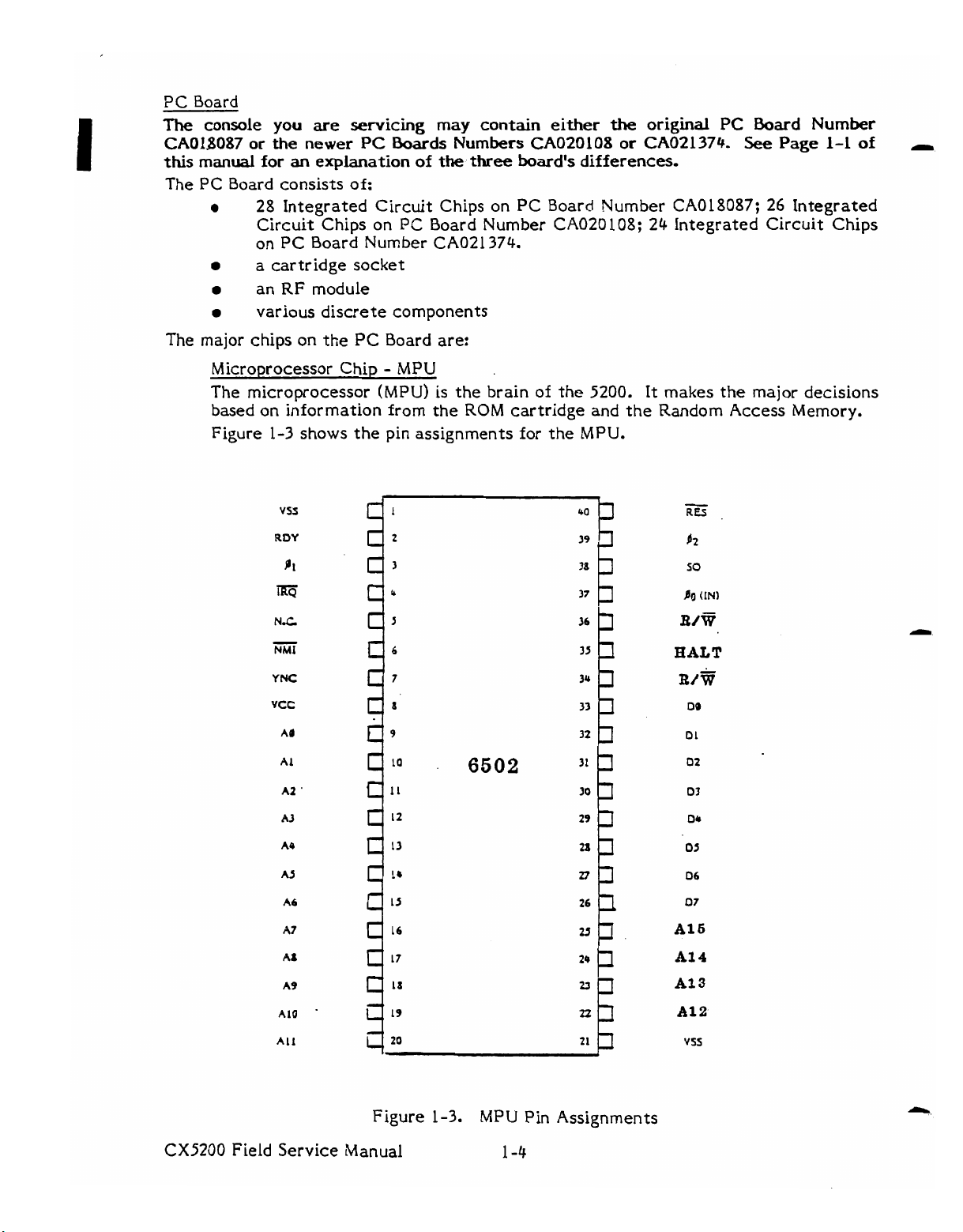
Microprocessor
The microprocessor
Chip
-
MPU
(MPU)
is the brain of the
based on information from the
Figure
1-3
shows the
VSS
ROY
P
1
pin
assignments for the
m
N.C
-
NMI
YNC
VCC
AU
A1
A2
'
A3
ROM
cartridge
MPU.
5200.
and
It
makes
the
major decisions
the Random Access Memory.
HALT
CX5200
Field
A4
AS
A6
A7
AS
A9
A10
'
A
11
Service
Figure 1-3.
Manual
MPU
Pin Assignments
1-4
Page 13
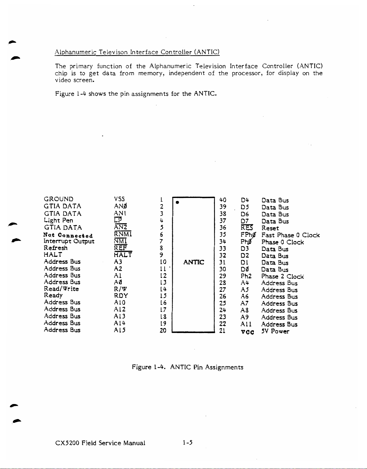
Alphanumeric Televison Interface Controller (ANTIC)
The
primary function of the Alphanumeric Television Interface Controller
chip is to get data from memory, independent of the processor, for display on the
video screen.
1-4
Figure
shows the pin assignments
for
the ANTIC.
(ANTIC)
GROUND
GTIA
DATA
GTIA DATA
Light
N0.t
Pen
GTIA
DATA
Connected
Interrupt Output
~efresh
HALT
Address
Address
Address
Address
Read/Write
Ready
Address
Address
Address
Address
Address
Bus
Bus
Bus
Bus
Bus
Bus
Bus
Bus
Bus
VSS
.4
NB
AN
1
c?
AN2
RNMl
A3
A2
A
1
Ad
R/W
RDY
A10
A12
A13
A14
A15
Figure
1-4.
ANTIC Pin Assignments
D4
D5
06
07
RFT
FPhg
pwf
D3
02
Dl
DB
Ph2
A4
A5
A6
A7
A8
A9
All
VCC
Data
Bus
Data
Bus
Data
Bus
Data
Bus
Reset
Fast
Phase
Phase
Data
Data
Data
Data
Phase
Address
Address
Address
Address
Address
Address
Address
5V
0
Bus
Bus
Bus
Bus
2
Power
0
Clock
Clock
Bus
Bus
Bus
Bus
Bus
Bus
Bus
Clock
CX5200
Field Service
Manual
Page 14

Graphic Television Interface Adaptor (GTIX)
The Graphic Televison Interface Adaptor
memory
registers. Figure 1-5 shows the pin assignments for the GTIA.
via the ANTIC
DMA
process.
(GTIA)
This data is routed to the GTIA graphics
chip retrieves graphics data from
-
-
Address
Address
Ground
Data
Dara
Oata
aata
Trigger
Trigger
Trigger
Trigger
Port
Port
+CAP
Not
Not
Color
Alphanum-
Alphanum.
Alphanum-
Bus
Bus
Bus
Bus
Bus
Bus
0
1
2
3
Select
Select
Control
Used
Connectad
Delay
Data
Data
Data
0
2
1
A1
A%
VSS
03
D2
Dl
Yf.
T1
T2
T3
sff
.
S1
s2.
53
..
DEL
AN0
AN
1
AN2
0
A2
A3
A4
Dk
D5
GTIA
06
D7
R/Y
m
LUM
a2
Fa'0
OSC
VCC
HALr
CSY
LUM
LUM
LUt.1
COL
Figure 1-5. GTIA Pin Assignments
o
NC
3
2
1
Address
Address
Address
Oata
Data
Data
Data
Read/Write
Chip
Luminance
Phase
Clock
Oscillator
Power
HALT
Output
Luminance
Luminance 2 Output
-
Luminance I Output
Color
Bus
Bus
Bus
Bus
Bus
3us
Bus
Select 1
o
2
Input
Out
Input
Sync
3
Output
Output
e
q
.
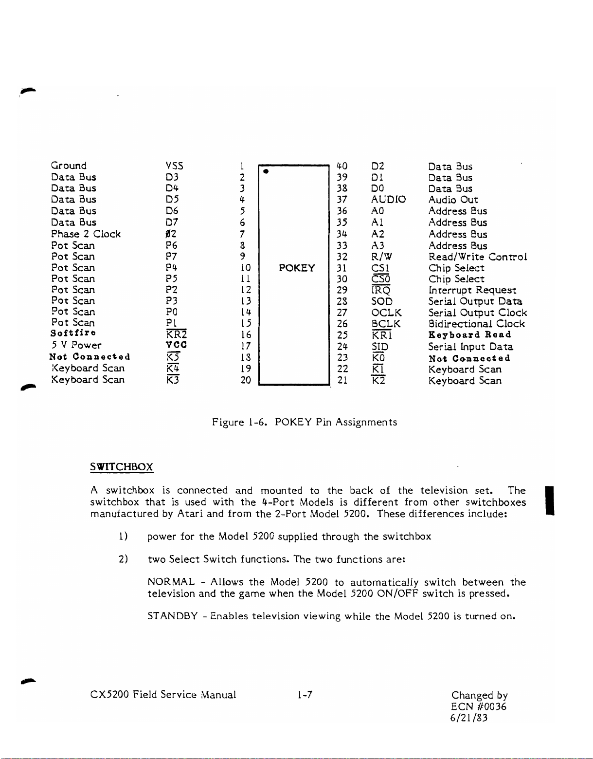
POT
Keyboard Integrated Circuit
The Pot Keyboard Integrated Circuit
game
channels, each with its own frequency, noise, and volume control. Figure
the pin assignments of
CX5200
ports and the microprocessor. It also contains four semi-independent audio
the
POKEY.
Field Service Manual
(POKEY)
(POKEY)
chip provides the interface between the
1-6
'
shows
Page 15
e
Ground
Bus
Data
Data
Bus
Data
Bus
Data
Bus
Data
Bus
Phase
Pot
Pot
Pot
Pot
Pot
Pot
Pot
Pot
Softfire
5 V Power
Not
:<ey
Keyboard
2
Clock
Scan
Scan
Scan
Scan
Scan
Scan
Scan
Scan
Connected
board
Scan
Scan
VSS
03
D4
D5
D6
07
#2
P6
P7
P4
P5
PZ
P3
PO
VCC
-
K5
i(4
K3
0
POKEY
D2
Dl
DO
AUDIO
A0
A1
A2
A3
R/W
CS
1
cso
-
IRQ
SOD
OCLK
BCLK
-
KRl
SID
K(;
K1
-
K2
Data
Bus
Data
Bus
Data
Bus
Audio
Address
Address
Address
Address
Read/Write
Chip
Chip
Interrupt
Serial
Serial
Bidirectional
Xeyboard
Serial
Net
Keyboard
Keyboard
Out
Bus
Bus
Bus
Bus
Control
Select
Select
Request
Output
Output
Read
lnput
Data
Cennec*ed
Scan
Scan
Data
Clock
Clock
Figure
A switchbox is connected and mounted to the back of the television set. switchbox that is used
by
manufactured
two Select Switch functions. The two functions are:
2)
NORMAL
television and the
STANDBY
CX5200
Field Service Manual Changed
Atari and from the 2-Port Model 5200.
with
-
Allows the Model
-
Enables television
1-6.
POKEY
the 4-Port Models
game
when the Model 5200
Pin Assignments
5200
viewing
is
different from other switchboxes
These differences include:
to automatically switch between the
while
ON/OFF
the Model
switch is pressed.
5200
is turned
ECN
/I0036
6/21
/83
The
1
on.
by
Page 16

GAME
The
12-key Keypad, two separate Fire Buttons on each side, and three Select Buttons. The
game controller is discussed in detail in Section
SUMMARY
CONTROLLER
game
controller supplied with the Model
5200
is composed of an analog joystick,
6.
a
-
The Model
Controllers, Read-Only-Memory (ROM) cartridges, and other peripherals. The console
PC
Board
interaction between the
the Alphanumeric Television Inter face Controller
Interface Adaptor
The console, switchbox,
is addressed in the remainder of this manual.
5200
is
an
advanced microcomputer which receives input from
is
housed within an outer
game
(GTIA),
and the
and
Game
case
and contains four major chips which allow for
and
the player. They are:
POT
Keyboard Integrated Circuit
Controllers
make
the
(ANTIC),
up the
Model
the
Microprocessor
the
Graphic Television
(POKEY).
5200
System which
Game
(MPU),
CX5200
Field
Service
Manual
Page 17

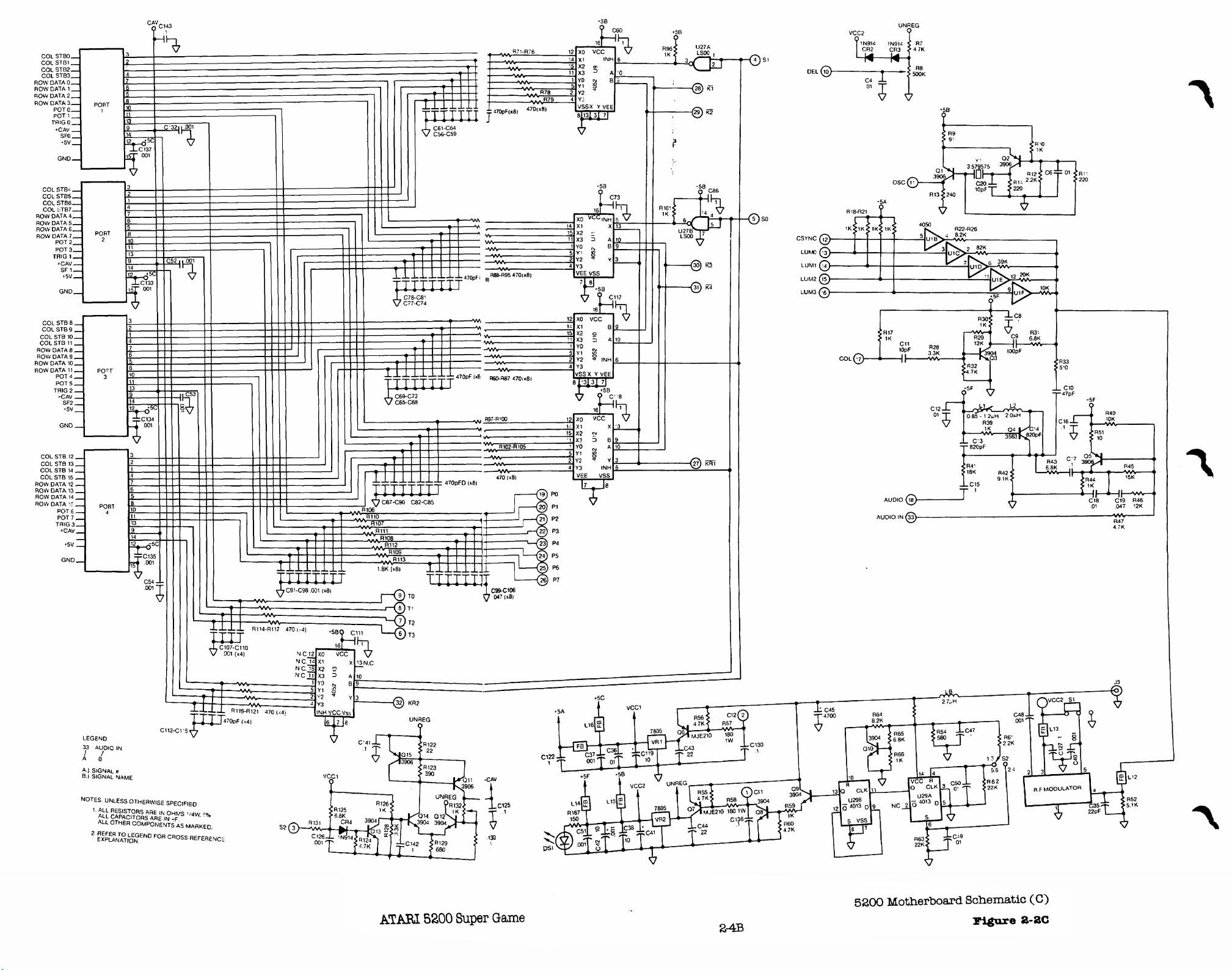
SILKSCREENS
On the following pages are representative silkscreens and schematics for the Model
5200.
of the unit, but these schematics provide
understanding of all Model
Minor variations in design
5200
may
units.
AND
SCHEMATICS
be encountered
all
details required for
depending
on the production date
an
in-depth
CX5200
Field Service
Manual
Page 18

Make pen
and
ink
corrections to schematics
on
pages 2-4 and
2-4B
as directed below.
1
,a
I
I
T-
I
-
I I
1;
IT.
Page
2-4
I
Remove connector line
Page
shown
2-4B
as
dotted line.
Page
2-40
Change
U298
Page
Add
SF3
+CAV
Port
4.
2-48
and
between
+5V
on
I
T
Page
Add
2-4B
ca~acitor
CX5200
Field
Service
Manual
Page 19

Page 20

Page 21

Page 22
Page 23

Page 24

Page 25

Page 26

I
continued
on
2-13
I
I'igt~re
2-4.
3
4
of
Port
4
Schematic
Page 27

Figure
2-4. 4 Port Schematic
4
of
4
Page 28
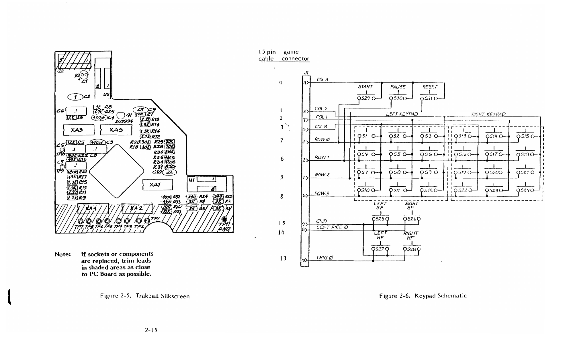
15
pin
cable
game
connector
START
PSZ9
PAUSE
RESk
Note:
If
sockets
are
replaced,
in
shaded
to
PC
or components
trim leads
areas
Board
Figl~t-e
as
as
possible.
2-5.
close
Trakball
Silkscreen
Figure
2-6.
Keypad
Sct
\errla
tic:
Page 29

bJ?J
XI*
I I
Page 30

Page 31

di-
Page 32

Page 33

DEL
CSYNC
LUMO
LUM
1
LUM
2
LUM
3
s-
+5
B
-
C12
.o
AUDIO
1
Page 34

Page 35

Page 36

SECTION
3
4-PORT
EQUIPMENT REQUIREMENTS
You require six basic pieces of equipment in order to analyze failures in the Model
5200. These items include:
15
MHz
oscilloscope
a
Diagnostic Cartridge (version
Model 5200 Port Board (Loop Back Board)
CX5200 Field Service Manual
a
color T.V. set (properly adjusted)
voltmeter
TESTING WITH THE DIAGNOSTIC CARTRIDGE (VERSION 1.1)
All
tests
given. If
troubleshooting.
OVERVIEW
The Diagnostic Cartridge (Version
you in identifying the source of problems
used in conjunction with the equipment listed
tests
are reviewed in this section. If applicable, a Flowchart Entry Point
a
failure occurs, go to the flowchart indicated and continue
OF
TESTS
available
in
the cartridge are:
MODEL
1
.I)
5200
TESTING
1.
I)
contains a variety of
in
the Model 5200. The
at
is
test
routines to assist
test
cartridge is
the beginning of this section. The
-
Color Bar
Gray Bar
Any Video
Pokey Adjust
RAM
Verify
Port
Tone
INITIALIZATION To prepare the Model 5200 for testing, perform the following steps in the order
given:
Connect the switchbox
Plug the power adaptor into the opening on the switchbox marked Power.
Plug the RF cable from the console into the opening on the switchbox
marked Game. Be sure the select switch on the switchbox is set to the
NORMAL position.
Plug the Model 5200 Port Board into rhe player ports.
Insert the Diagnostic Cartridge (Version 1.1)
Turn on the
CX5200
Field
OS
ROM
Service
to
the VHF terminah) on the back of the
ToVe
Set and the Model 5200.
Manual
3-1
TeVo
Changed
ECN
/I0036
6/21
/83
Set.
by
Page 37

The Model
5200
tests
are run using the Port Board (Loop
automatically cycles through all of
the Poit Board,
select any of the tests manually
NOTE:
is
inserted before the
plug
The
Diagnostic
a
game controller into Port 1, and turn
by
Cartridge
unit
is
Back
the
tests. If a test fails: turn the unit off, remove
the
unit back on. You
pressing the proper key followed
will
turned
cycle
on.
automatically
only
Board) which
by
the start key.
if
the
Port
can
Board
Press the * or
1
=Any
ill
key followed
Video
7=Ram
2=Color Bars 8=Verify
3=Gray Bars
4=Port Test
5=Pokey
Adjust
9=Display
O=
Examine
6=Tone Test
9
and
0
are
Options
not used
The following pages show the
If a test
fails,
go
to
the Flowchart Entry Point indicated for that
troubleshooting.
by
the start key to print this menu on the screen.
Test
OS
ROM
Options
at
this time.
tests
as they appear with the Port Board plugged in.
test
and
begin
CX5200
Field
Service
Manual
Page 38

POWER-UP
SCREEN
The Power-up screen appears in a few seconds.
It
displays information about the inner
workings of the unit. This screen shows:
The type of TIA in the unit.
a
for that unit. If PAL appears, replace with
0
The rev of
ROM
in the unit. (Not important
NTSC
appears if the
a
GTIA from your kit.
at
this time.)
GTlA
is the proper one
After the initial power-up, this screen do& not automatically appear again.
of
One
Solid
If a solid colored
catastrophic failure.
put
Diagnostic Flowchart Entry Point:
the following indicates a failure.
Solid Colored (Black) Screen or Vertically Lined Screen
a
a
Snowy Screen
a
Colored
WARPED - Ragged Picture
(Black)
Sueen
(Black)
or
Vertically
or
vertically lined screen appears, the unit
This means that the unit is not functioning well enough
up
a
simple display.
Lined
4-2.
keen
is
suffering
to
even
a
Snowy
Screen
If, when turned on the unit displays no modulation on the screen, the failure is
probably in the power circuitry.
a
Check that the select switch on the switchbox is set to the
However, first check the following:
NORMAL
position.
a
Check the power adaptor using
Diagnostic Flowchart Entry Point:
CX5200
Field Service Manual
Pg.
4-9.
standard voltmeter.
Page 39
Warped
-
Ragged
Picture
In this failure, the power-up screen appears bent to one side with
picture may roll or slide down and to the left of
by
signal broadcast
that the unit
the flowcharts.
Diagnostic Flowchart Entry Point:
COLOR
is
BAR
TEST
Purpose: To
a
operation.
Format: A screen of horizontal color bars displays (see Figure 3-1). . The
a
screen should
reference line runs across the screen about three bars from its bottom.
This reference line is thinner than the bars around it.
adjusted so the bars immediately above and below the reference line are
within one shade of each other.
by being able to make this adjustment
entire span of each bar on the screen. Minor glitches
color bars are acceptable. Leave this test on for
order
changing colors or blanking out.
the GTIA is probably not functioning.
not set on the same channel as the
Pg.
4-13.
test
the
GTlA
be
steady
to
catch any intermittent problems, such
chip and associated color circuitry for correct
and
the screen.
T.V.
set. Check this before going
unchanging.
Proper operation of the unit is indicated
and
This
Another possible cause is
A
gray or blue horizontal
by consistent color within the
at
as
a
ragged edge.
means
that the sync.
R8
should be
on
the edges of the
least ten seconds in
a
bar momentarily
The
to
CX5200
Field Service Manual
Page 40

NOTE:
This figure
is
a
black and white representation of a
color
television screen.
\
REFERENCE
f
Diagnostic Flowchart Entry Point: Pg*
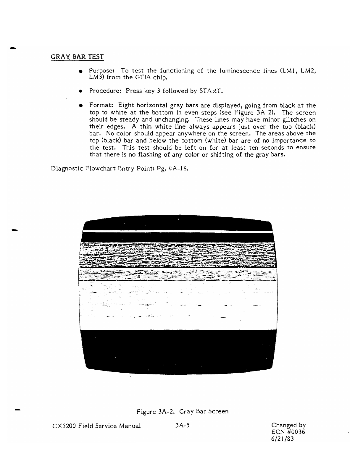
GRAY
BAR
TEST
Purpose: To test the function of the luminescence lines (LMO
from the
Format: Eight horizontal gray bars are displayed, going from black
0
top to white
should be steady and unchanging. These lines may have minor glitches on
their edges.
bar.
top (black) bar and below the bottom (white) bar are of no importance to
the
that there is no "flashing" of
BAR
Figure 3-1 Color Bars Screen
GTIA
No color should appear anywhere on the screen. The areas above the
test.
chip.
at
the bottom in even steps (see Figure
A
thin white line always appears just over the top (black)
This test should
4-1
4.
,
LM1,
3-2).
be
left on for at least ten seconds to ensure
any
color or shifting of the gray bars.
The
LM2)
at
the
screen
CX5200 Field Service Manual
Page 41

Figure
3-2.
Gray
Bar
Screen
Diagnostic Flowchart
ANYVIDEO
SCREEN
0
Purpose:
0
Format:
bars. Half of the vertical bars should be narrow, and the other half much
wider.
left to right, the shade of color on the horizontal bar should change.
the right of the bar, two Vs should be displayed, right side
CX5200
Field Service Manual
Entry
Point: Pg.
4-16.
To test the video generation of the
GTIA
and
ANTIC
chips.
The screen should have a black background with eight vertical
A
horizontal bar should appear across the top
of
the
screen.
up.
From
On
Page 42

NOTE:
Figure
3-3
is a black
and
white representation
of
a
colored screen.
Figure
If
the Any Video test fails, swapout
POKEY
CX5200
ADJUST
0
Purpose: To
0
Format: Adjust R132 to make
Field Service
check
+
1.
All other values should read between 100 and 124.
-
Manual
the value
3-3.
Any
Video Test Screen
U3,
U5.
of
the pot line for the controller ports.
in
the
value
Port 1,
HOR
position read
112
Page 43

NOTE:
Figure
may
3-4
shows a sample Pokey Adjust screen.
differ from those shown in Figure
3-4.
The
values
on
your screen
HOR
I
Figure 3-4. Pokey Adjust Screen-
Diagnostic Flowchart Entry Point: (Refer
ERROR
Errors during the
shown
SUMMARY
in
~i~ire 3-5.
RAM,
RROR
PORT, and verify
SUMMARY
VERT
to
Table 3-1, Diagnostic Error codes).
05
ROM
KB
Test are displayed on
the
matrix
-Number
Failure
Code Number
(Max.
of
99)
failures
Figure 3-5. Error Summary.
Table 3-1
shows the defective component and/or the flowchart entry point which
corresponds to the Failure Code number on the Error Summary.
CX5200
Field Service Manual
3-8
of
Test
Page 44

Table
3-1
Diagnostic Error Codes
Failure Code
Failure
RAM - Chip
RAM
-
Chip
1
-
U25
2 - U24
RAM - Chip 3 - U23
RAM - Chip
RAM - Chip
RAM - Chip
RAM -Chip
RAM - Chip
Port
1 - Data - Keyboard
Port
2 - Data - Keyboard
3 - Data - Keyboard
Port
4 - Data - Keyboard
Port
Trigger
Trigger
Trigger
Trigger
Soft Fire
Soft
Fire
Soft Fire
Soft Fire
0
1
2
3
0
1
2
3
4
-
U22
5
-
U21
6
- U20
7
-
U19
8 - Ul8
s
Reference
RAM Test, Pg.
I
I
11
I
I
11
11
11
I I
Page
f
3-10
Keyboard Troubleshooting
Pg.
4-21
11
Trigger Line Trouble-
shooting, Pg. 4-19
I I
11
I
I
Softfire Troubleshooting
Pg.
4-20
I
I
I I
11
Serial Port
Serial Port
Pot Line
Pot Line
Pot Line
Pot Line
Pot Line
Pot Line
Pot Line
Pot Line
0.S. ROM
0
1
2
3
4
5
6
7
0
1
-
US
CX5200 Field Service Manual 3-9
Not
Used
Not
Used
Pot Line Troubleshooting
Pgs.
4-17, 4-18
11
11
11
11
II
I I
II
Verify OS ROM,
Pg.
3-10
Page 45
RAM
TEST
.
Purpose:
Format: This
is solid
To test the 16K
test
takes approximately 10 seconds during which the screen
black.
At the end of this time period, if the
Failure Code number appears on the screen to signify which chip is
defective.
(Table 3-1).
U16,
U17, and U28 for
Swap out the chip corresponding to the Diagnostic Error Code
If
this does not solve the problem,
PCB
Al4, A15, A16 and A17.'
No Diagnostic Flowchart Entry Point
RAM
chips for proper functioning.
test
has failed,
swapout the chips U15,
KA018087. For PCB KA020108, swapout
a
VERIFY
OS
ROM
Purpose: To
0
0
Format:
OS
test
the
05
ROM
If
error code 30 appears on the Error Summary (Figure 3-5) the
ROM chip is defective. Replace the defective chip and restart the
No Diagnostic Flowchart Entry Point
PORT
TEST
0
Purpose: This
test
checks the functions of the POKEY,
associated PORT circuitry.
Format:
Summary (Figure
The test is done internally with failures appearing on the Error
3-5).
Diagnostic Flowchart Entry Point: (Refer
TONE
TEST
(U8)
for proper functioning.
to
Table 3-1, Diagnostic Error codes).
GTIA
test.
and
0
Purpose:
0
Format:
(Register 4,3,2,1).
To
check the audio generation section of the
The screen prints
A
series of eight tones will sound on each register. The
at
first two tones may be inaudible but you can hear the speaker click.
Diagnostic Flowchart Entry Point: Pg.
4-27.
CX5200 Field Service Manual 3-10
POKEY
(U7).
the bottom which register is being tested
Page 46

SECTION
3A
EQUIPMENT
2-PORT
REQUIREMENTS
MODEL
5200
TESTING
You require seven basic pieces of equipment in order to analyze failures in the Model
5200 2-port. These items include:
a
a
15
MHz
oscilloscope
Diagnostic Cartridge (version 1.1)
5200 Port Board (Loop Back Board)
0
0
CX5200
Field Service Manual
Color T.V. set (properly adjusted)
Volt-ohmmeter
0
TESTING
All of the tests are reviewed in this section.
Known-good 5200 controller
WITH
THE
DIAGNOSTIC
CARTRIDGE
(VERSION
If
a
test
1
-1)
failure occurs, enter the
diagnostic flow chart where indicated and continue troubleshooting.
OVERVIEW
The Diagnostic Cartridge (Version 1.1) contains a variety
in identifying the source of problems in the 5200.
conjunction with the equipment listed at the beginning of this section.
OF
TESTS
of
test
routines to assist you
The test cartridge is used in
The
tests
available in the cartridge are:
a
Color Bar
0
Gray Bar
Any Video
0
Verify
a
Tone
0
RAM
0
Pokey Adjust
OS
ROM
INITIALIZATION
To prepare the 5200 for testing, perform the following steps in the order given:
a
Connect the switchbox to the
VHF
terminah) on the back of the
T.V.
Plug the power adaptor into the console.
0
Plug the
marked
RF
GAME.
cable from the console into the opening on the switchbox
Be
sure the select switch on the switchbox is set to the
GAME/COMPUTER position.
CX5200 Field Service Manual
Changed
ECN
!I0036
6/21
183
set.
by
Page 47

a.
0
Plug a game controller into port 1 of the 5200.
Insert the Diagnostic Cartridge (Version 1.1).
Turn on the T.V. (Select Channel
2
or
3)
and the 5200.
Press the
*
or U key followed by the start
1
=Any Video 7=Ram Test
2=Color Bars 8=Verify
OS
ROM
key
to
display this menu
on
the
screen.
3=Gray Bars 9=Display Options
4=Port Test O=Examine
5=Pokey
6=Tone
#4
Test
To
and
run
the tests press the proper numerical key on the 5200 controller and then press
START.
press the bottom
Adjust
Test
0 are not used.
To
escape a test (except #5), press any
fire
button.
key.
To
escape
85,
POKEY
ADJUST,
The following pages show the tests as they appear with the Port Board plugged in.
If
a
test indicates a failure, go to the Flowchart Entry Point indicated for that
and begin troubleshooting.
POWER-UP
SCREEN
The power-up screen displays information about the internal status of the unit.
shows:
test
It
The type of
a
NTSC
a
The revision level
If
at
power-up this screen does not appear, one of the following screens appears:
Solid Colored (Black) Screen or Vertically Lined Screen
e
appears.
TIA
in the unit.
If
PAL
of
If
the GTIA is
appears, replace the
the
ROM
in the unit. (Not important
the
GTIA
proper
with one
Snowy Screen
a
Warped - Ragged Picture
Proceed to the description of that failure which follows.
CX3200
Field Service Manual
one
for the unit,
from
your kit.
at
this time.)
Page 48
GRAY
BAR
TEST
Purpose:
LM3)
0
Procedure: Press key 3 followed by
To test the functioning of the luminescence lines
from the
GTIA
chip.
Format: Eight horizontal gray bars are displayed, going from black
top to white
at
the bottom in even steps (see Figure 3A-2). The screen
should be steady and unchanging.
their edges. A thin white line always appears just over the top (black)
No color should appear anywhere on the screen. The areas above the
bar.
top (black) bar and below the bottom (white) bar are of
test.
the
that
there is no
This
test
flashing
Diagnostic Flowchart Entry Point:
should
of
Pg.
4A-16.
(LMl,
START.
These lines may have minor glitches on
no
importance to
be
left on for at least ten seconds to ensure
any
color or shifting of the
gray
bars.
LM2,
at
the
Figure 3A-2. Gray Bar Screen
CX5200 Field Service Manual 3A-5
Changed by
ECN
#0036
612
1/83
Page 49

ANY
.VIDEO
SCREEN
Purpose: To
a
Procedure: Press key 1 followed by START.
0
Format:
test
the video generation
The screen should have a black background with eight vertical
bars. Half of the vertical bars should
A
wider.
left
horizontal bar should appear across
to right the shade of color on
the right of the bar two
If
the Any Video tests fails, swapout
NOTE:
Figure
3-3
is a black and white representation
of
the GTIA and ANTIC chips.
be
narrow and the other half much
the
top
the
horizontal bar should
V's
should be displayed, right side up.
A3
and
A5, and restart the
of
a
test.
colored screen.
of
the
screen. From
change.
On
CX5200
Figure 3A-3. Any Video Test Screen
Field Service Manual 3A-6
Page 50

VERIFY
OS
ROM
To
test
0
Purpose:
0
Procedure: Press key 8 followed
the OS
ROM
(A8)
for proper functioning.
by
START.
Format:
0
3-8)
restart the
the
If
error code
OS
ROM
test.
chip is defective. Replace the defective chip and
No Flowchart Entry Point.
TONE
TEST
a
a
0
Purpose: To check the audio generation section of the
Procedure: Press
key
Format: The screen prints at the bottom:
1
followed by START. A series of eight tones sounds
The first two tones may be inaudible but you can hear the speaker click.
Repeat for registers
Diagnostic Flowchart Entry Point:
30
6
followed
2,3,4.
Pg.
appears
4A-17.
on
the Error Summary (Figure
by
START.
Register
(1
POKEY
to
on
(A7).
4)
?
each register.
3-1,
Press
pg.
key
CX5200
Field Service Manual
Changed
ECN
/I0036
6/21/83
by
,
Page 51

POKEY
(PORT)
TEST
Purpose: To determine any port line failures and confirm the correct
operation of the POKEY chip.
m
Procedure: Press
Format:
numbers and letters in the second column should
the
KEY
-
1 1
2
3
4
5
6
7
8
When
KB
column:
KBReadings
9
#
key
5
followed
you press the keys listed in the
2
3
by
START.
NOTE: When using
Cartridge to
KB
Readings may appear to the right
any of the four ports listed on the screen,
besides the port you are testing. They
must, however, appear to the right
-
port you
valid.
test
are
testing for
first column below, the
appear on the screen in
the 1.1 Diagnostic
the 2-PORT 5200, the
the
test
0
*
START
PAUSE
RESET
If the keys do not register correctly when pressed, proceed to
TROUBLESHOOTING, page 4A-22.
of
of
the
to be
KEYBOARD
Press the bottom fire button. The
If
Press key 5 followed
to the screen. Unplug the controller from Port
Repeat Step 2.
RAM
TEST
Initialization
Purpose: To
A25).
Procedure: Press key 9 followed
DISPLAY
screen.
RAM
Test
Procedure
Purpose: To
Procedure: Press key
it
doesn't proceed to page
by
for
RAM
Test
set
the
5200
Then press key
Again press key
ERRORS
test
CONTINUOUS TEST appears in the green band on the
the functioning of the 16K RAM chips.
7
POKEY
3A-9.
START,
up for a loop
2
2
followed
again bringing the
by
START.
followed by START.
followed
by
START.
by
ADJUST screen should disappear.
test
to fully
START.
POKEY
1
and
check
ADJUST pattern
insert it- into Port
the RAM
(A1
2.
8-
CX5200
Field Service Manual
3A-8
Page 52

0
For-mat: Each test lasts approximately ten seconds. The screen illustrated below
appears.
If
an error
is
listed on the screen, refer to Table
3-1,
page 3-9, to
determine which chip has failed.
POKEY
Failure
cod=
ERROR
Number
(Mu.
of
99)
SUMM
failures
Number
of
Tert
Figure 3A-4. RAM Test Screen
ADJUST TEST
Purpose: To test
+CAV
circuit output to the controller for proper
the
functioning.
Procedure: 1. Remove the PCB assembly from its plastic housing.
2.
Turn on the unit and press key 5 followed
by
START.
pot
CX5200
3.
Plug in
not plug into anything).
4.
Adjust R132 to make the value in Port 1,
The values on 1 VERT,
100 and 124, as illustrated below in Figure 3A-5. (Ports 2 and
have no bearing on the
1
2
3
4
Figure 3A-5.
Field Service Manual
the
loop back board (note that connectors 2 and 3 will
HOR
C
110
110
110
110 110
POKEY
4 HOR
test
VERT
107
~15
118
and 4 VER should read between
for the 2-port
KB
8
8
8
0
ADJUST Test Screen
3A-9
HOR
5200.)
position 112 21.
Changed by
ECN
#0036
6/21
/83
3
Page 53

If
the
unit
Entry Point:
cannot
Pg.
4A-20.
be
adjusted or
if
values
are
out
of
range, proceed to the Flowchart
POKEY
a
a
a
a
a
SOFTFIRE
Connect the oscilloscope to
Insert the controller into port
Press
Press
A
5v
SOFTFIRE
Unplug the controller from port
TEST
key 5 followed
the
top fire button (softfire).
p-p
square
by
wave
START.
signal should appear.
TROUBLESHOOTING
pin
1.
16
of
FLOW
1
and
A7
Repeat the fourth and fifth steps for port
(1v/division;l0ms/div.~.
If
it
does not,
CHART,
plug
it
page
into port
4A-19.
2.
2.
proceed
to
the
CX5200
Field
Service
Manual
Page 54
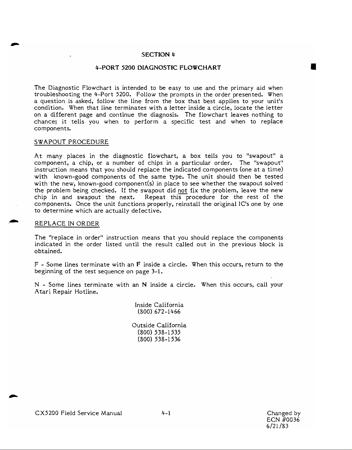
SECTION
4
4-PORT
5200
DIAGNOSTIC
FLOWCHART
The Diagnostic Flowchart is intended to be easy to use and the primary aid when
troubleshooting the 4-Port 5200.
a
question is asked, follow the line from the box that best applies to your unit's
Follow the prompts in the order presented. When
condition. When that line terminates with a letter inside a circle, locate the letter
on
a
different page and continue the diagnosis. The flowchart leaves nothing to
chance; it tells you when to perform
a
specific
test
and when to replace
components.
SWAPOUT
At many places in the diagnostic flowchart, a box tells you to "swapout"
PROCEDURE
a
component, a chip, or a number of chips in a particular order. The "swapout"
instruction means that you should replace the indicated components (one
with known-good components of the same
type.
with the new, known-good component(s) in place to
the problem being checked.
chip in and swapout
If
the swapout- did
the
next. Repeat this procedure for the rest of the
The unit should then
see
whether the swapout solved
fix the problem, leave the new
at
be
a
time)
tested
.
components. Once the unit functions properly, reinstall the original IC's one by one
to determine which are actually defective.
1'
REPLACE
IN
ORDER
The "replace in order" instruction means that you should replace the components
indicated in the order listed until the result called out in the previous block is
obtained.
F
-
Some lines terminate with an F inside a circle. When this occurs, return to the
test
beginning of the
N
-
Some lines terminate with an N inside a circle. When this occurs, call your
i
Atar
Repair Hotline.
sequence on page
3-1.
Inside California
(800)
672-1466
Outside California
(800) 538-1535
(800) 538-1536
CX5200 Field Service Manual
Changed
ECN
/I0036
6/21
/83
by
Page 55

w
Is
there
signal
a
1.78975
on
Pin
I
Swapout
1) U5
2)
U3
29
No
MHz
of
Black
U3?
Yes
'
k
No
Screen
Troubleshooting
I
output
4
Is
MHz
Is
there
signal on Pin 28
I
Is
there
signal on Pin
of
there
signal on
of
a
3.5795
a
3.57950
VRl?
Yes
a
1.78975
US?
I
No
I
I
Yes
I
29
I
Pin
MHz
of
MHz
of
30
U5?
U5?
#
b
I
No
w
Pg.
pg.
4-4
4-3
b
Open between
Pin
I
Repair
*
t
29
&
U3
Pin
m
Open between
U2
Pin
37
and
U3
Pin
m
or
Replace
US
35.
34.
No
is
there
a 3.57950
signal
on
Pin 35
Is
there
a
1.78975
signal
on
Pin
a
on
I
1.78975
Pin
I
No
Is
there
signal
d
0
34
37
Yes
of
of
of
MHz
U3?
MHz
U3?
MHz
U2?
Page
No
I
4-5
Swapout
1)
U3
2)
U2
J
*+*NOTE"++
If
you
are servicing a unit containing
PCB
CA020
been changed
108,
from
chip
designators have
U
to
A.
CX52C)O
Field Service Manual
Page 56

Black
Acreen
Are
the
voltages on the pins
of the. transistor:
Troubleshooting (Cont.)
following
Qr
Base
Emitter 4.3V 4.3V
Collector 1.2V
3SV
42
3*5V
1V
1
Yes
No
I
Replace
I
transistor(s). correct?
J
Are voltages
I
b
Yes
I
Y1.
Yes
.
No
l
L
Check
shorted or wrong
clock circuit.
1
Repair
for open,
or Replace
Replace
Q
Does unit
function? value component
B
'
in
I
1
CX
If you are servicing a unit containing
PCB
been changed from
5200
Field Service
CA020
108,
chip designators have
U
to
A.
Manual
Page 57

alack
Screen
Troubleshooting
(Cont.)
I
Is there approximately yes
11-1
3V
on the input of
VRl?
No
A
Is there approximately
0
V
on pintaof the
schematic?
I
Defective
2)
R57
Rep
air
b
N~
b
Defective
output
ground (possible
Defective J1 or open
between pointaof
VR2
&
point@of
(with cartridge
VRl
short to
chip)
or
ViZl
in).
-
CX
5200
Field
Service Manual
P
If
you are servicing a unit containing
PCB
been changed
CA020
108,
chip designators have
from
U
to
A.
Page 58

alack
Screen
Troubleshooting (Cont.)
a
Open between
U2
and
and
Pin
Repair
0
1
Pin
29
30
of
Pin
of
U5.
39
U3
.-
PCB
CA020108,
been
changed
c6ip
from
designators
U
to
A.
ha;e
'CX5200
Field
Service Manual
Page 59

PCB
Q
m
b
"-
g
E
2
2
2
U
U
-
-
1
U1
.A2 U2
.A3
U3
U
c
A5 U5
36
U6
A7 U7
A8
U8
A9 U9
410
1JlO
\I1
till
A12
:JL2
A13
lJ13
A14
U14
U
,416 U16
A17 U17
A18
UlS
A19
U19
A20 U2O
A21 U21
A22
U22
A23
U23
,424 U24
A25
U25
U
A27
U27
U2S
U
A15
A26
15
26
29
Not
used
14
14
I
C
I4 7
14
7
7
7
7
Black
i
Screen
Is
there
chips?
Is
Pin
Troubleshooting (Cont.)
40
I
+5V
(See
I
I
of
I
(
I
I
chart)
Yes
U2
Yes
Yes
to
at
all
SV?
9
No
b
Swapout
I)
U2
2)
U3
3)
U5
4)U8
5)
U7
.
NO
L
Repair
chip
(Check
w
Defective
Reset
connected
open
&
+5
for
circuitry
to
between
or ground.
bad
socket)
U1
or
other
,
U2
Pin
40.
L
Rephce
-
1
Repair
or
CX5200
Field
Service Manual
L
Is
problem
Page
I
repaired?
No
4-7
'
If
you
PCB
been
yes
are
CA020
changed
*+*NOTE**"
servicing a unit containing
108,
chip
designators have
from
U
to
A.
Page 60

Black Screen
Troubleshooting (Cont.)
I
Is
there a data signal
on Pin2of U18-U25?
+'
Is there a data
signal on Pin 14
of U18-U25?
I
I
Swapout
1) Ul4
2) U15
3)
U16
4) U17
I
Yes Is there
-
n
I
display?
Defective:
1 ) U28 (CAO 18087'only)
2)
L4-L6
4)
Open Address
line
to
RA,M
Repair
or
Yes
Yes
a
good
Replace
J
'
Paae 4-8
I
1
No
Open Trace RAM
chip Pin 2 to U2
Or
replace defective
a
If
only one chip
missing signal, replace
that chip. If not,
proceed.
I
Does unit function?
Is
there
4V
p-p
6
U18
RAM
8
of U14
of U28?
1
Yes
a
4V p-p
Pin
-
U25?
chip(s) to
on Pin
I
Is there
signal on
Swapout
1) Ul4
2) U28 or Open Pin 4
of
Pin
RAM.
is
signal
4 of
P
1
b
I
B
Yes
1
Repair
Defective:
i;fcL6
3) C30-33
A
Repair
or
Replace
4
I
b
1
J
w
e
is
I
4+
b
c
CX5200
there a good
display?
Swapout U18-U25
Field Service Manual
I
If
you
are servicing a unit containing
PCB
CA020108,
been changed
chip designators have
from
U
to
A.
Page 61

Black
Screen Troubleshootinq (Cont.)
4
Is
there
signal on
J
w
I:
Swapout
1) U17
2)
Ul4
R133,C140,R68
I
&
If
you are servicing a unit containing
PCB
been changed from
a
4V
p-p
Pin
15
of
U
l8-U25?
No
.
or
defective
C55
CA020108, chip designators have
U
7
b
to
A.
CX
5200
Field Service Manual
Page 62
Snowy
Screen
(Do
Troubleshooting
.
Is
C48
good?
not
short
across)
'
No
I
r
I
Is
there
the
+5
RF
I
Is there +12 volts
input
of
Page 4-12 No
Does Pin 13 of
change between 13V
bc
OV
when
is pressed?
Press
1
S2
3
on Pin 3 of
Module?
I
on
VR2?
~29(~26)*
S2
Yes
so
that
Pin
is
high.
1
yes
I
I
I
No
Defective
1)
L13
2)
RF
Module or open
between
module
Page 4-1 1
Pin
&
2
RF
VCC2.
*U29
on
PCB
A26
on
PCB
I
is
chip
fCA018087
is
chip
#CA020108
Repair
I
or
~e~lace
b
designation
designation
CX5200
Field Service Manual
If you
PCB
are
servicing a
CA020
108,
chip designators have
been changed from
U
unit
containing
to
A.
Page 63

Snowy
Screen
Troubleshooting
7
(cont.)
I
Is
there OV on the
collector of
1
Is
there
base and
emitter of
13V
14V
I
Yes
I
Defective
Repair
'Replace
QS?
on the
on
the
Q7?
No
1
Defective
Defective
1)
47
2)
R55
3)
R58 or
open trace to
collector
48
or
of
Q9.
Q8.
-
rn
CX 5200
Field Service
Manual
If
you
are servicing a unit containing
PCB
CA020108, chip designators
been changed from U to A.
have
Page 64

Snowy Screen Troubleshooting (cont.)
I
Does Pin
Does Pin 6 of
high when
11
is
pressed?
released?
or
defective
Repair
of
I
~29(~26)*~o
52
is pressed
opens
52.
toggle each time
and low when it
shorts
the failing pin or
~29(~26)*
2
52
is
on
1s
pin
LO
of
U29(A26)
OV?
Is there continuity
between Pin
of
~29(~26)*
I
Replace
U29(A26)
9
&
12
n
*
at
*
5--
-
No
'
Replace QI
Repair trace.
0
Doesunitwork?
L
Open trace
defective resistor
or capacitor in
4
circuitry.
or
2
I
Repair
or
Replace
*U29
on
A26
on
is
chip
PCB #CA018087
is
chip
PCB
#CA020108
designation
designation
If
you are servicing a unit containing
PCB
CA020
been changed from
108,
chip designators have
U
to
A.
CX5200
Field Service Manual
Page 65

Snowy Screen Troubleshooting (cont.)
m
Is
there
+5v
on the
output of
If
Pin
3
VR2
short to ground:
Possible short
1
chips one-by-one and
If
modulation occurs,
VR2?
I
in
chips. Remove
turn
on unit.
bad
chip has
been located. If chips are not
shorted, check for possible
CAP
trace shorted on board.
Yes
or
Repair
Open
Pin
3
VR2
VCC2,
to
+5B or +5F.
0
r
Replace
2
If
you
are
PCB CA020108, chip designators
been changed from
J
b
servicing a unit containing
have
U
to
A.
CX
5200
Field Service Manual
Page 66

A
-
Warped
Open between Pin 4 of
A1
&
R22
Ragged
I
Picture
Manually set 5200 on
Is
there a +5 p-p signal
on the leg of
connected to Pin
Is
there a +5V p-p
signal on Pin 4 at Ul?
Troubleshooting
R22
4
I
Is
Yes
module
or L 12 or open be
tween R22
R22
good?
I
&
RF
Replace
module
-
Repair
-
4
b
Defective U1 or
power or ground to Ul.
Pin
no
Open between U5
25 and Ul Pin
5.
Is there a +5V p-p
signal on Pin 5 of Ul?
Is
Yes
w
there a +5V
signal on Pin 25
of
U5?
Swapout:
2) U2
3)
U3
p-p
A
If
you
PCB
been
are
servicing
CA020
changed
108,
***~O~*+*
a
unit
containing
chip
designators
from
U
to
A.
have
CX5200
Field Service
Manual
Page 67

Color Troubleshooting
*
Manually
color bars pattern.
4
h
Is
L
Does
adjust between
6
justed to
4
volt
I
set
frequency of
3.5795.
Pin
volts when R8
adjusted.
6V
p-p
21
of
unit onto
I
I
I
I
17
of
is
there
signal
U5?
Y1
U5
0
on
and
is
a
pin
No
L
v
Replace
Defective
1)
2)
Y
R8
CR2
1
1
b
CX
Is
there
signal
5200
(
I
a
2
between
&
R28?
(
Page
Field
Yes
volt
p-p
C11
Yes
4-I
Service Manual
No Defective
b
If
you
PCB
CA020108,
been changed
d
are
servicing
open
Cll
chip
from u to
4-14
C11
or
to
U5
Pin
a
unit
containing
designators
A.
21.
'
have
I
-
Repair
or
Replace
r
Page 68

Color Troubleshooting (cont.)
I
Is
there a .4v p-p
signal on the base
of Q3?
1
1
Yes
I
Is there a 4v p-p
signal on the collector
of Q3?
I
I
yes
3
Is there a
,-
signal between
and R31?
volt p-p
C9
No
b
No
Defective R28 or open
I
I
Yes
to
R30
'
at
Trace R28
IS
the signal present
approximately
Defective
43..
OV?
I
No
b
Defective
R29.
I
1
Yes
1
Mistuned R.F. Module
or defective:
1)
R31
2)
RF
Module or open
R31
to
R.F.
Module
4.
Pin
J
Defective
I
C9
C9
or open
to the collector
If
you are servicing a unit containing
PCB
CA020
been
changed from U to
108,
chip designators have
A.
CX
5200
Field Service Manual
Page 69

Gray
Bars Troubleshooting
Manually set the
5200 to the Gray Bars
I
att tern.
I
If
you
PCB
been
are servicing
CA020108,
changed
chip designators
from U to
a
unit
containing
A.
have
1
Is
signal on the side of
R23,
Connected to
I
Reference the line
on
which has the resistor
that did not have the
I
there a +5V p-p
R24,
&
No.
the chart below
proper signal.
I
Is
there
a
signal on the
output pin?
2
Is there a +5V p-p
signal on
+5V
I
No
the
input pin?
I
R25.
U
1
?
p-p
U1
U1
B
b
I
A
Yes
Yes
yes
Defective
R25
or open between
R23,R24, or
R.F.
Module Pin 4.
Open between
put
and
L
Defective
+5V or ground
to
R23,R24,
R25
and
U1
U1
out-
or no
that resistor.
U1.
-
I
b
CX
5200
Line
Field
Swapout
2)
U2
3)
U3
#
Resistor
Service Manual
Repair
or
#
Replace
US
Pin
#
I
#
Ul
Output
U1
Input
Pullup
Page 70

Pot
Control
I
Line
Troubleshooting
Manually set the 5200
to the Pokey Adjust
defective port be
adjusted between
4-6.4V
R
Can
1
32?
test.
+CAV
by
I
on
turning
I
L
Swapout
I
Do pot lines pass?
I
From Error Code on
below
chart
which line
&
check the compo-
nents for correct
a
Do POT Lines pass?
is
value.
m
determine
defective
-
I
If
PCB
Yes
been changed
No
you
are
servicing
CA020
Open or shorted
108,
trace.
a
unit
containing
chip designators have
from U to
A.
Repair
CX
POT
Line
Error
Code
22.
23
24
25
26
27
-
28
29
5200
Field Service
Pokey
Failure
HOR
VERT
HOR
VERT
HOR
VERT
HOR
VERT
Manual
Adjust
1
1
2
2
3
3
4
4
Port
Pin
and
li
Pokey
Pin
U7
#
CAP
#l
CAP
#
2
Resistor
R106
R110
R107
Rlll
R108
R112
R
109
R113
Page 71

Pot Control Line Troubleshooting(Cont.)
L
4
Can
i
Lhec~
Ql
1414
I
readings to the ones
shown for the
Are
J
I
Swapout
1)
U5
2)
U7
+CAV
be
now?
I
the
voltages on
and
condition in the
I
the readings
correct?
adjusted
compare
"A"
J
'
I
No
If
you
are servicing a unit containing
PCB
CA020108,
yes
,
Replace rransistor. Does Pokey Adjust
been changed
chip
from u to
designators
A.
pass?
I
have
Yes
-
Put unit into Port Test
node but do not put in
Port board (loop
board).
I
Check the voltages on
Q11
-QL
4
and
readings to the ones
shown for the
condition on the
chart
below.
Condition/
Transistor
Emitter
Base
Cdlector
4-6.4V
back
compare
"B"
Ql
1
A
13V
12V
B
13V 3.2V
13V
OV
A
4V
13V
No
Are the readings
correct?
Ql2
OV
OV
13V
-
A A
0
0
3.SV
Ql3
yes
A
0
.7V
OV
Defective component
in
Pokey Adjust
I
circuitry.
Repair
I
Check
shorts
3.2V
3.
12V 13V
for opens
in
repair.
Q14
'
circuitry
0
OV
OV
&
Jc
I
-
CX
5200
Field Service Manual
Page 72

2)
3)
US
Socket
Cap
on that line.
See
chart*
Trigger Line Troubleshooting
Bottom' Fire Button
Is the
US
pin
defective Port at
volts with everything
unplugged
Plug
for the
+5
from the Port?
in
controller.
u
-
Is
pin still at
I
+5V?
I
Defective controller.
-
Push
bottom fire button.
Does
and hold
I
signal drop to
approximately
0-.7
volts?
I
Yes
Defective
0
U5
'
i
Port
Is
trigger line
shorted to
I
Yes
U5
Pin
+5V?
#
Cap
No
#
CX
5200
Field Service Manual
If
you are servicing a unit containing
PCB
CA020
been changed from
108,
chip designators have
U
to
A.
Page 73

Softfire (Top Fire
F'
Insert Diagnostic cart-
ridge into console.
Insert Game Controller
into Port
manually
ad
Are there
waveforms at
I
I
Depress & hold soft
I
fire button. Is
1.
select Pokey
just test.
-
Pins
1,2,4
Pin 3 pulsing?
I
Button)
5V
p-p
U13
&
5?
Yes
U13
Yes
Troubleshooting
I
h
J
No
Are there
forms at
I
Are there
waveforms at
Pins
&
12-
5V
p-p wave-
U13
LO?
No
5'V
&
13?-
I
Pins
f
Yes
9
J
p-p No
U5
J
Replace
I
Replace
U
1 3
U5
I
I
I
b
Swapout and retest*
the
following order:
I)
u7
2)
U3
3)
U5
2
If
PCB
been changed
in
~ote:@
1
check Pin
Port
Port
2
check
Port 3 check Pin
Port
4
check
you
are
servicing a unit containing
CA020108,
With softfire button
1
IYes
held down9 are there
sv
wavefdrms
Pin
Repair open trace
from
U13
I
Pin
Fin
4,
2,
5,
1,
Pin
U13
U13
U13
U13
16?
Pin 3 to
.,
chip designators have
from
U
to
A.
16.
at
~7
U7
I
I
A
CIWC*
U13
below).
Check for opens from Repair
and
I
waveform at
Pin
@
Is
pin
to
game
(see
chart
it now low?
(see chart)
port plug
controller
1
yes
-1
Replace
U13.
CX
5200 Field Service
fvlanual
Page 74

Keyboard Troubleshooting
Is
the failure
on
Port
I?
Manually
Adjust
Are there
waves
on
U9-U1
Which
select
Test.
5v
Pin
port
Pokey
p-p
square
9
.&
10
2?
failed?
of
J
No
Replace
I
U7.
6
CX5200
Field
Service
Manual.
0
Paee
4-24
-0
-
-.
If
you
PCB
heen
+**~O~~***
servicing a unit
are
CA020
changed from
108,
chip designators
U
containing
to
A.
have
Page 75
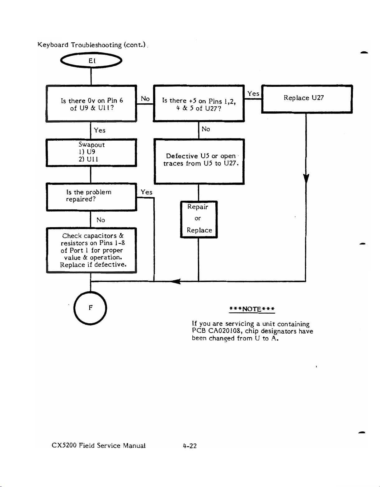
Keyboard Troubleshooting (cont.)
1s there Ov on
of
U9
&
Ull?
Pin
6
No
.
Vac
Is
there
4
t5
on Pins l,2,
&
5
of
U27?
1
1
Yes
Is
the problem
repaired?
i
Check capacitors
resistors on Pins
I
of Port 1 for proper
&
value
I
1
Replace if defective.
operation.
&
1-8
b
Yes
I
I
I
I
Defective
traces from
US
or open
US
to
.
U27.
CX5200 Field Service Manual
If you are servicing
PCB
CA020 108, chip designators have
been
chansed
from
a
U
unit
containing
to
A.
Page 76

Keyboard Troubleshooting (cont.)
I
Swapout
Does
Port
2
r
Check capacitors and
on
resistors
of
Port
value
Replace
Pins
2
for proper
&
operation.
if
defective.
pass?
1
-8
1
CX5200
Field
Service
Manual
If
you are servicing a unit containing
PCB
CA020
been
changed from U to
108,
chip designators
A.
have
Page 77

Keyboard Troubleshooting (cont.)
I
Swapout
1)
UlO
Does
2). U11
Port
3
pass?
L
d
u
I
Check capacitors
resistors
of Port
def
3.
ec
on
Pins
Replace if
the.
I
J
&
1-8
-h
If
you are servicing a unit containing
PCB
CA020
been changed
108,
chip designators have
from
U
to
A.
CX5200
Field Service Vanual
Page 78

Keyboard Troubleshooting (cont.)
Swapout
1)
UlO
2)
u12
4
Does Port
pass?
17
I
Check capacitors
I
resistors on Pins 1-8
of
Port
4.
Replace if
defective.
Y
I
1
CX5200
Field Service Manual
If
you are servicing a unit containing
PCB CA020 108, chip designators have
Seen
changed from
U
to
4.
Page 79

Keyboard Troubleshooting (cont.)
Are signals missing on
U9
and/or U11 only?
Yes 1)
Swapout
2)
3)
U27
U9
Ul1
v
I
Replace
b
n
If
you
are
servicing a unit containing
PCB CA020108,
been changed from
chip designators have
U
to
A.
CX5200
Field Service Manual
Page 80
Adjust
Replace:
I)
L1
2)
L2
Audio Troubleshooting
I
Is
there a
4.5
Can
LI
be
Is
there
adjusted
Mhz
1
+5VDC
Q4?
Replace:
1)
C13
2)
Cl4
give a 4.5
on the collector
I
to
reading?
L
of
No
on
*
With audio
is there a wries of
changing square waves
on
Is
the
approximate same
series of signals
visible
between
R4l?
Is
there a 4.5
pq
signal
CIO
connected
of
the emitter
of
Q4?
I
test
U7
Pin
1
Yes
Mhz
on
the side
Mhz
goin3
37?
C15
to
I
-2v
&
Q4?
NO
Swapout
I)
U7
2)
U2
Defective
U7
Pin
37
C15
4
'
A
A
Does audio
work?
Yes
*If
second
time
at
this
step,
call
ATARI
Repair
Yes
I
Defective:
1)
ClO
2)
R33
Hotline.
If
PCB
been
I
Repair
Of
Replace
you are servicing a unit containing
CA020
changed from U to
108,
chip
designators
have
A.
CX5200
Field Service
Manual
Page 81

SECTION
4A
2-PORT
The Diagnos
troubleshooting the 2-Port 5200. Follow the prompts in the order- presen-ted. When
a
question is asked, follow the line from the box that best applies to your unit's
condition. When that line terminates with a letter inside
on
a
different page and continue the diagnosis. The flowchart leaves nothing to
chance; it tells you when to perform a specific
components.
SWAPOUT
At many places in the diagnostic flowchart, a box teils you to "swapout"
component, a chip, or a number of chips in a particular order. The "s~apout'~
instruction means that you should replace the indicated components (one at
with known-good components of the same type.
the new, known-good component(s) in place to see whether the swapout solved the
problem being checked.
in and swapout the next. Repeat this prozdure for the rest of the components.
Once the unit functions properly, reinstall the original IC1s one by one to determine
which are actually defective.
REPLACE
tic Flowchart is intended to
PROCEDURE
IN
ORDER
5200
DIAGNOSTIC
be
If
the swapout did not fix the problem, leave the new chip
FLOWCHART
easy to use and the primary aid
a
circle, locate the letter
test
and when to replace
a
The
unit should then
be
tested with
w
time)
lhen
a
The "replace in order" instruction means that you should replace the components
indicated in the order listed until the result called out in the previous block is
obtained.
F
-
Some lines terminate with an F inside a circle. When this occurs, return to the
beginning of the test sequence on page 3A-I.
N
-
Some lines terminate with an N inside a circle. When this occurs,
Atar i Repair Ho tline.
Inside California
(800) 672-1466
Outside California
(800) 538-1 535
(800) 538-1536
*
call
your
CX5200 Field Service Manual
Changed
ECN
/I0036
6/21
/83
by
Page 82

IC
#
-
A1
.4
2
A3
A5
A6
A7
A8
A9
A10
All
A14
A15
A16
A17
A18
A19
A20
A21
A22
A23
A24
A25
A27
BLACK
Gnd
-
8
1,21
1
3
8
1
12
8
8
8
7
7
8
8
16
16
16
16
16
16
16
16
7
SCREEN
Is
Pin
40
I
Is
Pin
5
Is
problem
TROUBLESHOOTING
I
Yes
I
of
A2
Yes
I
36
of
A3
1
(
Yes
Swapout
I
repaired?
at
at
5V?
5V?
N~
I
Repair
Defective
N~
L
d
P
,
reset
ed
Open
Pin
open
between
A1
or
other
circuitry connect-
to
A2
pin
40,
Pin
36
of
A3
40
of
A2.
to
I
-
D
-
Repair
Rep
lace
Yes
CX5200
No
Field Service Manual
Page 83

BLACK
SCREEN
TROUBLESHOOTING
(Continued)
Is there approximately
9V
on
the
input of
VRl?
1
Is
there approximately
9V
on pointaof the
schematic?
Defective
2)
R57
Repair
L
yes
r
Defective
I
..'
output short
ground (possible
chip)
Defective
between poinaof
VR2
&
(with
poinaof
cartridge in).
VR1
J2
or open
or
to
VR1
1
-
b
CX5200
Field
Service
P
Manual
Changed
ECN
#0036
6/21
/83
by
Page 84

BLACK
SCREEN
TROUBLESHO(M1NG
1
(continued)
Gnd
-
8
1,21
1
3
8
1
12
8
8
8
7
7
8
8
16
16
16
16
16
16
16
16
7
Is
Pin
Is
Is
there
chips?
40
Pin
36
Swapout
1)
2)
3)
4)
5)
(See
of
of
A2
A3
A5
A8
A7
+5V
i
I
Yes
i
A2
1
1
Yes
1
A3
Yes
to
ail
chart)
at 5V?
at
5V?
A
b
b
N~
No
No
Repair
I
chip
(Check
Defective
reset
ed
to
Open
Pin
open
&
+5
or
for
bad
A1
circuitry
A2
pin
Pin
36
40
of
A2.
between
ground.
socket)
or
other
connect-
40.
of
A3
to
-
-
Repair
Replace
CX5200
Field
Service
Manual
Note:
Some
5200 2-port boards have pins
of
A7
PCB.
Do
not
jurnpered
Future
add these jumpers
together
PCB's
will
on
the
incorporate
solder
to the
5200 2-port board.
1,8,9,10
side
this
jumper.
and
of
11
the
Page 85

BLACK
SCREEN
TROUBLESHOOTING
(~ontinued)
Are
voltages on
of
the transistor:
Base
I
Emitter
Collector
I
the following
the
pins
ol
sz
305~ 3JV
4.3V
4.3V
1.2V
Replace
1V
I
1
Yes
Y.1.
0
I
Does unit
function? value component
Yes
B
No
b
>
N,
Replace
transistor(s).
J
Are voltages
correct?
I
Check
shorted or wrong
for open,
clock circuit.
J
in
rn
CX5200
Field Service
Manual
Repair
I
or
Replace
Changed
ECN
/I0036
6/21
/83
by
Page 86

BLACK
SCREEN
TROUBLESHOO'TING
(Continued)
h
IS
signal
I
there
Open
A2
and
a
on
between
and
Pin
Pin
Repair
1.78975
Pin
39
i
I
29
30
of
of
Pin
of
A5.
0
MHz
A2?
39
A3
N,
Y
Swapout
1)
A2
2)
A3
3)
A5
CX5200
Field Service
Manual
Page 87

Whenever the flowchart directs you
procedure
again directed
in
Section
to
3.
enter
Proceed until another error
the
flowchart or
operational.
to
F,
return to
until
the
the
beginning of the testing
is
encountered and you
unit
has
proven to
be
are
fully
P
CX5200
Field Service
Manual
Changed
ECN
/I0036
6/21
183
by
Page 88

BLACK
SCREEN
TROUBLFcHOOT'WG
(Continued)
b
Is
there a data
on Pin 2 of
1
A18-A25?
1
I
Isthere a data signal
on Pin
I4
of
A1 8-A25?
Yes
Swapout
1)
A14
2)
A15
3)
A16
4) A17
b
display?
Defective:
1) A15
2)
L4-L6
3)
C30-33
4)
Open
Address
I
Repair
or Replace
signal
>
No
Open Trace
chip Pin 2 to
or replace
defective RAM
I
No
L
If
only one chip is
missing signal, replace
RAM
A2
Repair
A
that chip, if not proceed
D
b
Does
L
Is
there
on Pin 9 of
Is
signal
A
unit function?
No
4V
p-p
Al??
there
a
4V
on
1
Pin 4 of
8-A25?
signal
p-p
'
I
I
,
Yes
No
L
1
Replace
A17
J
Swapout
1) A14
2) A15
or open Pin
of
RAM
8
of
chip(s)
A14
I
Pin
4
to
CX5200
Field
Is
there a good
Service
Manual
Page 89

BLACK
SCREEN
TROUBLESHOOTING
(continued)
4
Swapout
replace defective
C30-33, L4-6. A1
A15
or
N~
*
L
Is
there
signal
a
on
8-A25?
4V
Pin
I
1
Swapout
1) A17
2)
A14
or
defective
R133,Cl40,
&
C55
Yes
p-p
15
of
R68
-
CX5200
Field
Service
Manual
4A-9
Changed
ECN
/I0036
6/21
/83
by
Page 90

SNOWY
b
Is
LED
+
on?
SCREEN
(POWER
SUPPLY)
TROUBLESHOOTING
h
Is
there
on the output of
b
VR2 or
the
Is
there
pin
R.F.
at
on the input of
+
L
Is
the base
0.7-1
.OVDC less
than the emitter?
/'
L
Is
the collector of
Q8
&
at 0 volts?
No
5VDC
3
of
modulator?
I
(
No
least
+7VDC
VRZ?
of
47
No
1
I
r
D
J
A
Yes
Yes
Yes
Yes
1
Defective
I
open
from
VR2.
#
Defective VR2 or
shorted output
I
+
b
q
Defective
Defective
broken trace to
*
LED
LED
47.
R58
or
to
VR2.
or
a
47.
w
I
r
L
J
I
7
L
I
I
I
CX5200
No
Field Service
[Manual
Replace
Repair
I
or
Page 91

SNOWY
SCREEN
(POWER
SUPPLY)
TROUBLESHOOTING
(Continued)
1
Is
there
gnd
on
pin
1
of
R.F.
i
module?
No
L
Open
to
R.F.
ground.
pin
1
L
I
(
b
Yes
Defective
1)
R.F.rnodule
2)
R.F.
Cable
3)
J3
).
J
I
CX5200
Field
Service
Manual
Changed
ECN
/I0036
6/21
/83
by
Page 92
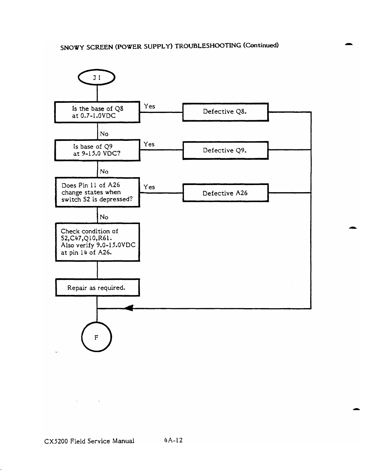
SNOWY
SCREEN
(POWER SUPPLY)
TROUBLESHOOmG
(continued)
L
IS
at
F
I
the
base
0.7-1.OVDC
I
Is base
J
at
1
Does
change
switch
2
I
Check condition of
S2,C47,Q1O,R6le
Also
at
pin
verify
I
(
9-15.0
Pin
states
S2
14
of
11
is
of
I
I
NO
of
depressed?
I
9.0-15.OVDC
A26.
of
Q8
Q9
VDC?
A26
when
Yes
A
Yes
b
Yes
I
I
I
I
L
J
L
J
Defective
Defective
Defective
Q8.
Q9.
A26
.
i
J
I
i
r
CX5200
Repair
Field
as
required.
1
Service
Manual
Page 93

WARPED,
RAGGED
PICTURE
TROUBLESHOOTMG
Repair
1
Open between Pin 4 of
A
1
and
R22.
Manually
power
I
Is
there a
on
the leg
ed to Pin
Is
there
signal on Pin
-
+5
of
4
a
set
up
p-p
R22
of
Al?
+5V
4
5200
on
screen.
signal
connect
p-p
at
Al?
I
J
Yes
L
,
i
odule
[S
R22
or
L12
good?
or open
No
L
be-
I
No
r
A
T
4
Defective
power or ground to
2
Open between
pin
25
and
A1
~1
or no
A5
pin
AL.
5.
Yes
4
Is
there
a
+5V
a
+5V
p-p
p-p
25
signal on Pin 5 of
1s
there
signal on Pin
of
Al?
A5?
CX5200
Field
Service
Manual
Changed
ECN
M036
6/21
/83
by
Page 94
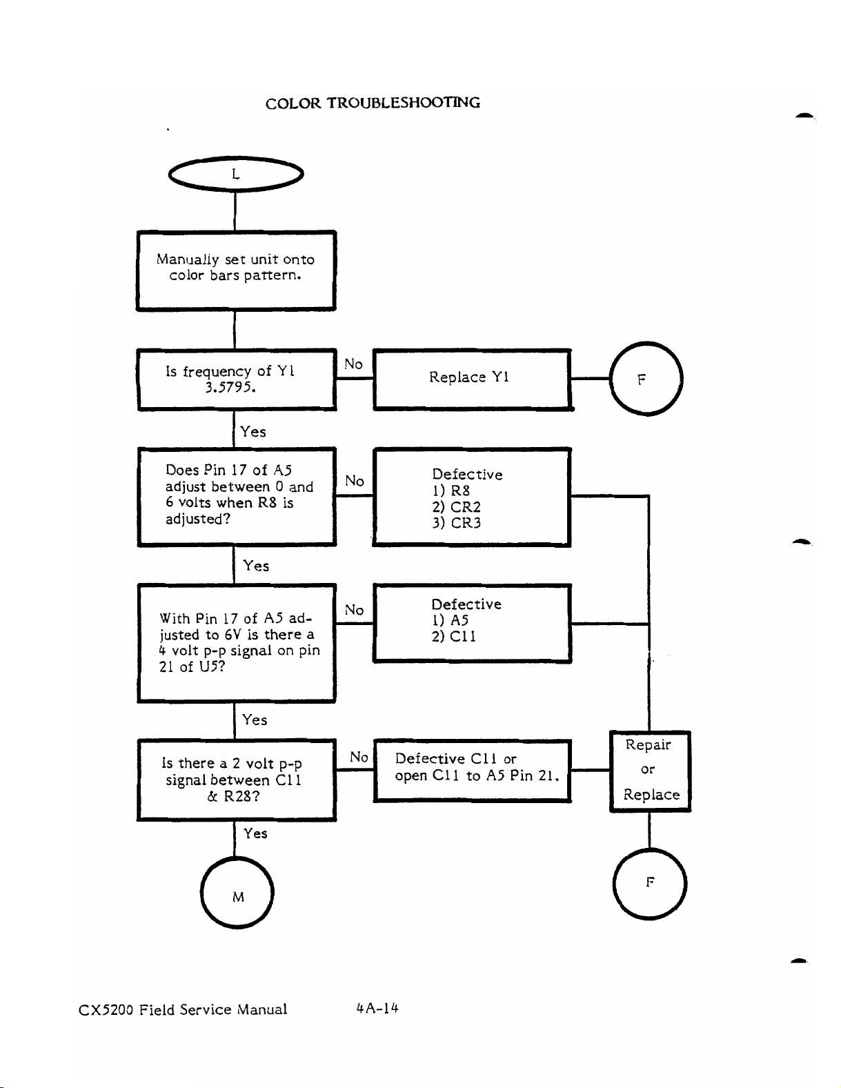
COLOR
TROUBLESHOOTING
Is
frequency
3.5795.
J
b
Does
Pin
adjust between
6
volts
adjusted?
i
I
With
Pin
I
iusted
to
I
of
1
1
Yes
I
17
of
when
R8
1
Yes
17
of
6V
is
I
Yes
Y1
A5
0
and
is
A5
ad-
there
a
I
I
L
No
No
""
I
1
Replace
Defective
1)
R8
2)
CR2
3)
CK3
Defective
Y1
J
.
L
CX5200
Is
there
signal
a
between
&
I
Field Service
2
volt
R28?
1
Yes
Manual
p-p
C11
Defective
open
Cll
C
to
1
1
A5
or
Pin
21.
Replace
Page 95

Is
signal
I
there a
on
of
Q3?
.4v
the
1
Yes
COLOR
p-p
base
TROUBLFHOOmG
Defective
Trace
R28
R28
or
to
(Continued)
open
43.
I
-
n
Is there
signal
Is
there
signal between
Mistuned R.F. Module
or
defective:
1)
R31
2)
RF
R31
Pin
a
4v
p-p
on
the collector
of Q3?
I
Yes
a
3
volt
p-p
C9
or R31?
Module or open
to R.F. Module
4.
Is
the signal present
at approximately
Defective
Defective
I
C9
to the collector
I
Yes
R30
C9
OV?
or open
Defective
R29.
t
CX5200
Field
Service Manual
Changed
ECN
//0036
6/21
/83
by
Page 96

GRAY
BARS
TROUBLESHOOTING
5200
I
to the Gray Bars
pattern.
I
Repair\
i
is pullup resistor
good?
Yes
Swapout
1)
A5
2)
A2
3)
A3
I
3
>
Is
there a
signal
R26,R24, & R25
nected to
Reference the
on the chart below
which has the resistor
that did
Is
signal on the
output pin? resistor.
1s there
signal
input
L
1s there a
signal on the
+5V
Al?
not
have the
+5V
a
c5V
on the
pin?
1
I
+5V
p-p
A1
A1
P-P Yes, Open between
A5
on the side of
proper signal.
there a
con-
line
p-p
p-p
pin?
H
9
yes
h
ye,
I
'
b
.
Defective
R25
or open between
R26,R24,
R.F.
Module
Open between
output and that
t
Defective
+5V
or ground to
Al.
and
A1
-
R26,R24
or
input.
d
Repair
1
or
Replace
R25
Pin
A1
A1
A5
and
4.
or no
pin
I
t
I
I
I
A
CX5200
Field
Line
"The
Service
#
1
.1
Manual
0
Resistor
Diagnostic Cartridge does not test
#
4A-16
*l
Output
A1
LIMO.
Input
Pullup
#
A5
Pin
#
Page 97

Adjust
AUDIO
Can LI be adjusted to
4.5
give a
-f
Mhz reading?
Is there
t5VDC
the collector of
1
Yes
Replace:
1)
C13
2)
C14
3)
Q4
4)
CR8
5) CR7
TROUBLESHOOTING
Is there
signal on the emitter
of Q4?
Yes
+With
audio test
going
is
there a No Swapout
series of changing
square
waves on
Pin
37?
Is
the approximate
same series of signals
visable between
R4
on
Q4?
L
a
4.5 Mhz
111
I
1
Yes
l?
A7
CIS
&
I
b.
,
I
l)A7
2) A2 work?
b
)
M
open
A7
37
and
Pin
C15.
Does
No
audio
9
+If this
the
ATARI
is
your second time at this step, call
Repair Hotline (see page 4A-1).
Is there a 4.5
p-p signal on the side
Mhz
I
-2v
1
yes
Defective: Repair
I)
C10
2)
R33
I
CX5200
Field
Service
Manual
Changed
ECN
/I0036
6/21
/83
by
Page 98

(See
Chart Below)
Defective:
1)
A5
2)
Socket of
3)
Cap
on
that
TRIGGER
A5
line
LINE
J
NO
-
h
(BOTTOM
Is
the
defective port at
volts with everything
unplugged from the port?
(see
FIRE
A5
pin for the
chart below)
in
Plug
controller.
BUTTON)
+5
P
TROUBLESHOOTlNG
Is
pin
still at
&5V?
Defective controller.
I
Push
bottom fire button.
Does signal drop to
4
and hold
Is
trig er line
approximately shorte%to+ZV? CheckRlllorR117
0-1
volt? for open.
I
I
Yes
Defective
A5.
0
Pwt
A5Pin#
I
Yes
Cap#
t
I
'No
Res
#
CX5200
Field
Service
Manual
4A-18
Note:
Some
of
A7
PCB. Future PCB's
Do
not
5200
2-port
boards
have
pins
jumpered together on the solder
add these
will
jumpers
incorporate
to the
1,8,9,lO
5200
side
this
2-port
and
of
the
jumper.
board.
11
Page 99
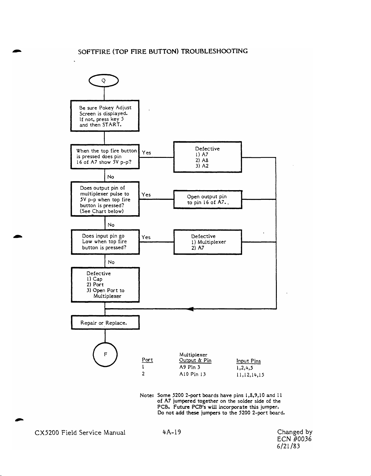
SOFTFIRE
Be
sure
Screen
If
not, press key 5
and then
I
(TOP
Pokey
is
displayed.
START.
Adjust
FIRE
BUTTON) TROUBLESHOOTING
L
When the top fire button
is
pressed does pin
16 of
Does output pin of
multiplexer pulse to
5V
button is pressed?
(See Chart below)
Does input pin
Low
I
A7
show
5V
p-p?
I
p-p when top fire
when
Defective
1) Cap
2)
Port
3)
Open Port to
go
top fire
A
yes
Yes
L
Defective
1)
2)
3)
Open output pin
to pin 16 of
I
Defective
1)
2)
A7
A8
A2
A7.,
Multiplexer
A7
CX5200
I
Field
Repair or Replace.
Service
Manual
Port
-
1
2 A10 Pin 13 1 1,12,14,15
Note: Some 5200
of
PCB.
Do not add
Multiplexer
Output & Pin Input Pins
A9
Pin
3
2-port
A7
jumpered together on the solder side of the
Future
PCB's
these
boards
will
jumpers
192,475
have pins 1,8,9,10 and 11
incorporate this jumper.
to
the 5200 2-port board.
Changed
ECN
#0036
6/21
/83
by
Page 100
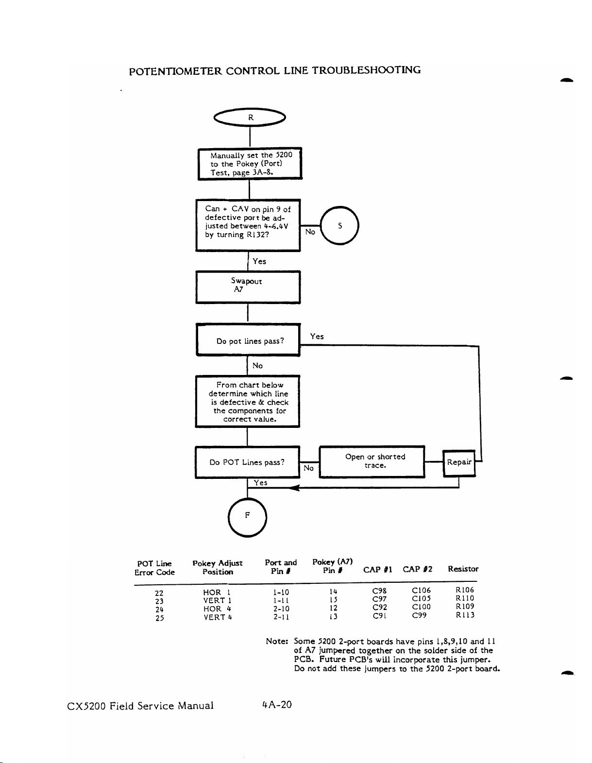
POTENTIOMETER CONTROL
to
the
Pokey (Port)
Can
+
CAV
on
1
Yes
pin 9 of
be
defective port
justed
between 4-6.4V
by
turning R1 32?
LINE
ad-
TROUBLESHOOTING
POT
Error
Line
Code
22
23
24
2
5
and
#
1
1
A
No
Yes
4
Pokey
Pin
Open or shorted
(A71
#
15
12
13
Do pot lines pass?
J
From chart below
determine which line
is
defective
the
components for
correct value.
Do
POT
Pokey
Adjust
Position
HOR 1 1-10 14 C98
VERT
1
HOR
4
VERT
4
&
Lines
check
pass?
Port
Pin
1-1
2-10
2-1
trace.
CAP
#I
CAP
C97 C105
C92
C9
1
P
-
Repair
I
#2
Resistor
C106 R106
C
100 R109
C99
RllO
R113
CX5200
Field
Service
Manual
Note: Some 5200 2-port boards
of
A7
jumpered together
PCB.
Future
Do not
PCB's
add
these jumpers to the 5200 2-port
will
have
pins
on
incorporate this
1,8,9,10
the solder side of the
jumper.
and
board.
11
 Loading...