

Page 1

2600/2600
A
VCS
DOMESTIC
(MD)
Field
Service
Manual
FD100133
Rev.
02
Page 2
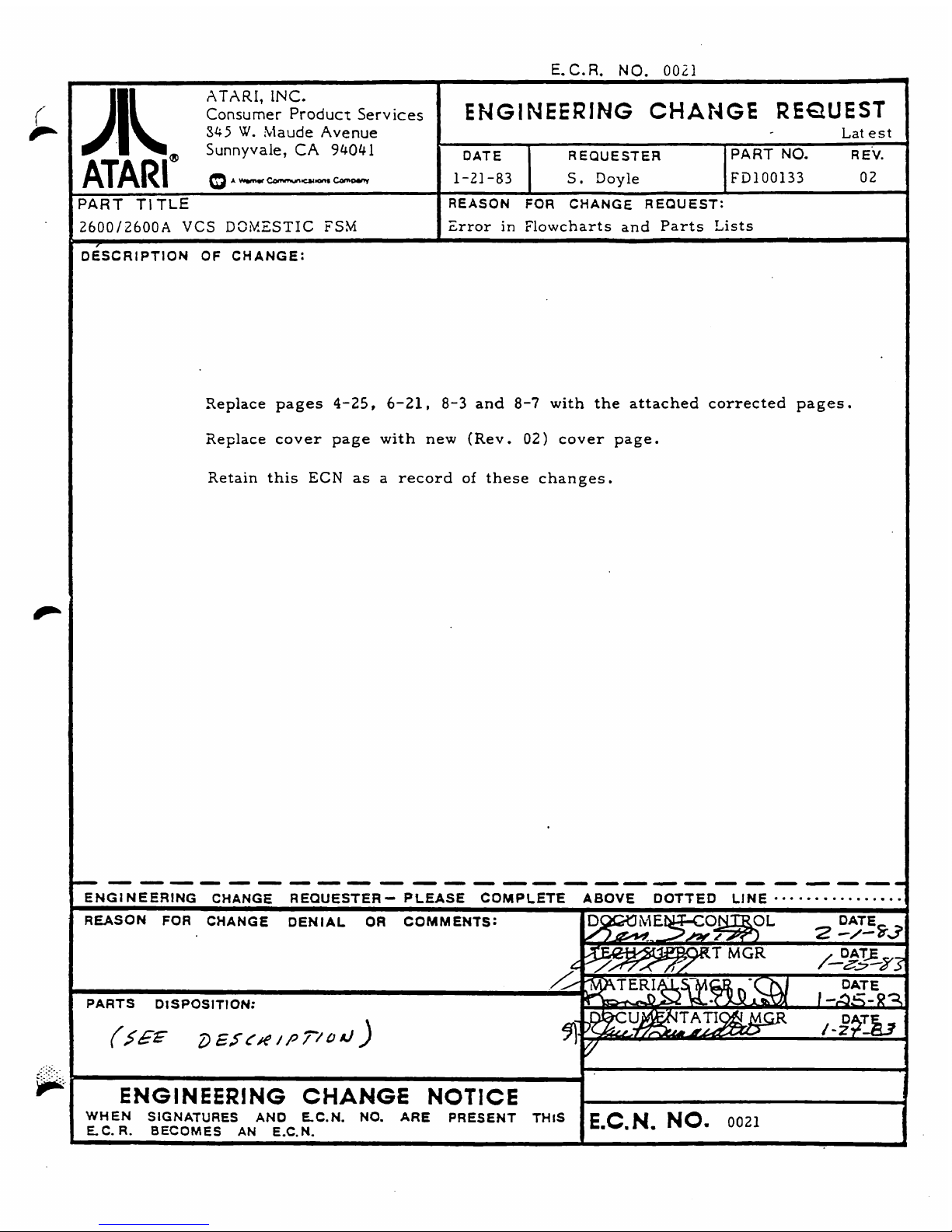
E.C.R.
NO.
0021
2600/2600A
VCS
DSMZSTIC
FSM
I
Error
in
Flowcharts
and
Parts
Lists
JR
ATARI,
INC.
consumer
Product
Services
845
W.
Maude Avenue
Sunnyvale,
CA
94041
ATAR~
o~------
PART
TITLE
Xeplace
pages
4-25,
6-21,
8-3
and
8-7
with
the attached corrected
pages.
Re~lace cover
page
with new (Rev.
02)
cover page.
Retain
this
ECN
as
a
record of
these changes.
ENGINEERING
CHANGE
REQUESTER-
PLEASE
COMPLETE
ABOVE
DOTTED
LINE
***
***
****-•
=-
(SEE
D~s~H/~~la~)
ENGINEERING
CHANGE
REQUEST
Lat
est
ENGINEERING
CHANGE
NOTICE
I
WHEN
SIGNATURES
AN0
LC.N. NO.
ARE
PRESENT
THIS
EmC,Nm
NO.
0021
E.C.
R.
BECOMES
AN
E.C.N.
I
PART
NO.
R
EV.
Fill
00133
02
DATE
1-21
-83
REASON
FOR
CHANGE
REQUEST:
REQUESTER
S.
Doyle
Page 3

ATARI
VIDEO
COMPUTER
SYSTEMTM
FIELD
SERVICE
MANUAL
MODEL
2600/2600A
DOMESTIC
(M/N)
Page 4

Atari believes that
the
information described in this manual is accurate
and
reliable,
and much
care has been taken
in
its preparation. However,
no
responsibility, financial or otherwise, shall
be accepted for
any
consequences
arising out of
the
use
of
this material. Information contained
herein
is
subject
to
change.
Revisions
may
be
issued to advise of
such
changes
and/or additions.
Correspondence regarding this document
should
be forwarded
to
Manager
of
Technical Support,
Consumer Product
Service,
Atari, Incorporated,
845
W.
Maude
Sunnyvale, California
94086.
2600/2600A
Domestic
VCS
Page 5

Table
of
Contents
P
Section
Title
-
Page
INTRODUCTION
THEORY
OF OPERATION
Introduction
Overview
Game Console
Outer Casting
Switchboard
:Motherboard
2600A Model Differences
-
All Revisions
2600A Model Differences
-
Revisions
14
and
15
2600A Model Differences - Revisions
16
and
up
Summary
2 SCHEMATICS
AND
SILKSCREENS
3
TESTING
AND
TROUBLESHOOTING
Equipment Requirements
Test Procedures and Methods
2600
Model Modifications
2600A Model Modifications
Testing with the Diagnostic Test Cartridge
(Version 2.6)
Initialization
RAM Test
Color Bar Test
Gray Bar Test
magnostic Matrix Test
Audio Tones Test
Paddle
Control
Lines Test
2600 DIAGNOSTIC FLOWCHART
SYMPTOM
CHECKLIST
2600 Symptom Checklist
2600A Symptom Checklist
2600A DIAGNOSTIC FLOWCHART
GAME
CONTROLLERS
Overview
Joystick
(X-Y)
Controller
Joystick
(X-Y)
Controller Check
Paddle Controller
Paddle
Controller Check
Driving Controller
Driving Controller Check
Keyboard Controller
Keyboard Controller Check
ATARI
CX2600
(M/N)
PARTS
LIST
ATARI CX2600A
(M/N)
PARTS
LIST
iii
2600/2600A Domestic
VCS
Page 6

Table
of
hntents
Section
9
Figure
Title
-
SERVICE BULLETINS
List
of
Illustrations
Title
-
2600
Functional Diagram
2600
Game
Console
2600
Switchboard and Motherboard Assembly
TV
Switchbox
2600A
Game Console
2600A
Board Layout
2600/2600A
IC
Pinouts
2600
Motherboard Silkscreen
2600
Channel 3 Switchboard Silkscreen
2600
Channel 3 Switchboard Schematic
2600
Channel
2-3
Switchboard Silkscreen
2600
Channel
2-3
Switchboard Schematic
2600A
Motherboard Silkscreen (Revs. 1-1
3)
2600A
Motherboard Silkscreen (Revs. 14
and
15)
2600A
Motherboard Silkscreen (Revs.
16
and
up)
Inserted
in
Front
Pocket
of
Notebook:
2600
Motherboard Schematic
2600A
Motherboard Schematic (Revs. 1-1
3)
2600A
Motherboard Schematic (Revs. 14 and 15)
2600A
Motherboard Schematic (Revs. 16
and
up)
2600
Trigger Circuitry with Static Modification
2600
Static Modification Zener Diode
Location of Colored Dot Over Trace
2600
Switchboard Static Modification
2600A
(Revs. 1-1
3)
Static Modifications
Switch Initialization Positions
Defective
RAM
Patterns
Color Bars Screen
Grav
Bars
Screen
~iagnostic Matrix Screen (Shorting Plugs
OUT)
Diagnostic Matrix Screen (Shorting
Plugs
IN)
Audio Tone Test Screens
Page
9-1
Page
iv
2600/2600A
Domestic
VCS
Page 7

List
of
Illustrations
(Continued)
Figure
Title
Page
Table
-
4-1
Switch Initialization Positions
Color
Bars
Screen
Defective
RAM
Patterns
Gray
Bars
Screen
Defective Gray
Bars
Screen
Diagnostic
Matrix
Screen (Shorting Plugs
OUT)
Diagnostic
Matrix
Screen (Shorting Plugs
IN)
Diagnostic
Matrix
Screen with Defective Pattern
Audio Tone Test Screens
RC
Waveforms
STC Address Line Waveforms
STC Data Line Waveforms
Joystick
(X-Y)
Controller
Joystick
(X-Y)
Schematic
Paddle Con troller
Paddle
Confroller Schema tic
Driving Controller
Driving Controller Schematic
Keyboard Controller
Keyboard
'Xriring Diagram
Keyboard Schematic
4
List
of
Tables
~iile
Connected Pins on
VCS
Motherboard
Page
4-47
2600/2600A
Domestic
VCS
Page 8
sections:
a
a
a
0
0
a
a
a
.
a
INTRODUCTION
The Video Computer systemT' (VCS) Field Service Manual is organized in nine
THEORY
OF
OPERATION
-
overview of how the VCS works and what the
basic assemblies look like.
SILKSCREENS
AND
SCHEMATICS
-
electrical drawings and layouts
of
the
printed circuit boards.
TESTING
AND
TROUBLESHOOTING
-
overview of the procedures
for
testing and repairing the VCS unit.
2600
DIAGNOSTIC
FLOWCHART
-
thorough flowchart enabling
the
technician to
test
and troubleshoot a defective
2600
unit.
SYMPTOM
CHECKLIST
-
for the experienced technician, a list of the high
failure parts and the flowchart entry point for that particular problem.
2600A
DIAGNOSTIC
FLOWCHART
-
thorough flowchart enabling the
technician to
test
and troubleshoot a defective
2600A
unit.
GAME
CONTROLLERS
-
overview of hand controller construction with
electrical schematics and recommended
test
and repair procedures.
PARTS
LIST
-
detailed breakdown of all parts used in both the
2600
and
2600A
.
SERVICE
BULLETINS
-
section to be used to hold service bulletins released
by the Manager of Technical Support. These bulletins will include changes
in recommended repair procedures and required modifications for units in
the field.
The manual is designed for use by both experienced and inexperienced service
personnel.
The
Diagnostic Flowcharts (Sections 4 and
6)
provide detailed diagnostic
and repair procedures for technicians who are not yet completely familiar with the
VCS. The Symptom Checklist (Section
5)
provides a fast repair reference for
the
more
experienced technician.
2600/2600A
Domestic
VCS
Page 9

SECTION
1
THEORY
OF
OPERATION
There are currently four types of ATARI Video Computer Systems. The original model
(2600) is composed of two
PC
Boards connected by a 12-pin ribbon cable with the
motherboard surrounded by a heavy aluminum casting.
The
other models (2600A: Revisions 1-13, Revisions 14-15, and Revisions 16
and up)
are composed of a single board with a light aluminum shield. The single board models
differ slightly in the video output circuitry.
Component differences are:
Revisions 1-1 3 have no diodes on TIA lines LA41 and Sync.
a
Revisions 14-15 have diodes and pull-up resistors on TIA lines LMl
and
Sync.
e
Revisions 16
and
up include the above mentioned diodes and resistors
as
well as a timer chip.
The revision level
is
etched directly on the
PC
board.
OVERVIEW
The ATARI Video Computer System (VCS) Models 2600/2600A are state-of-the-art
microcomputers. They receive instructions for the operation of different games from
individual Read-Only-Memory game cartridges and interpret data from the players'
hand-held controllers. They
also
allow game players to select both a specific version
of
each
game and the player difficulty (on a per player basis). Figure
1-1
is a block
diagram of the functional flow of the
VCS
Model 2600. Section 7 describes the player
controllers.
-
.
brar
Ellmcutor
(AX,
Adwmrt
120
VAC
Figure
1
-1.
2600
Functional Diagram
2600/2600A Domestic
VCS
Page 10
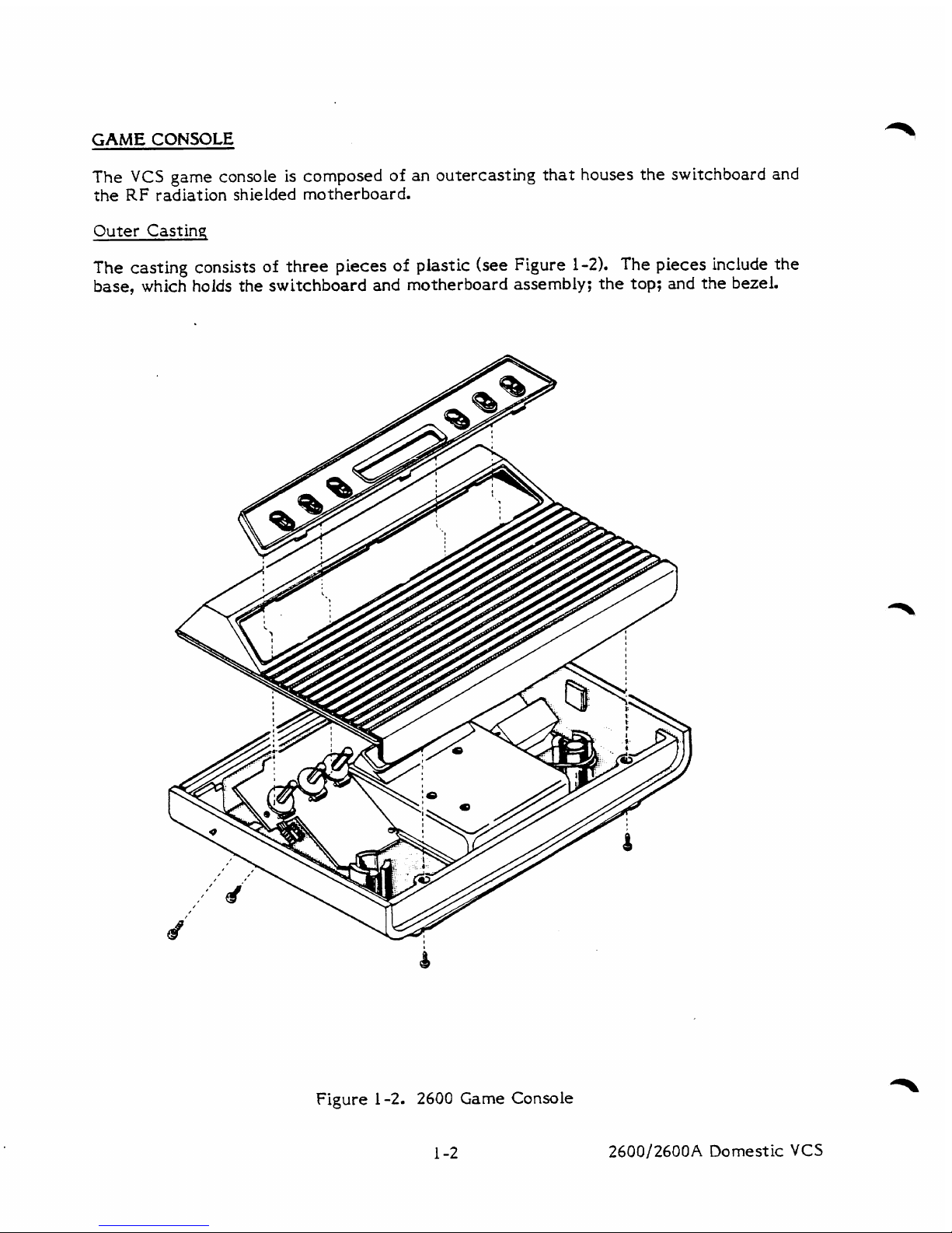
GAME
CONSOLE
The
VCS
game
console
is
composed
of an
outercasting
that
houses
the
switchboard
and
the
RF
radiation
shielded
motherboard.
Outer
Cast
inq
The
casting
consists of
three
pieces
of
plastic
(see
Figure
1-2).
The
pieces
include
the
base,
which
holds
the
switchboard
and
motherboard
assembly;
the
top;
and
the
bezel.
Figure
1-2.
2600
Game
Console
2600/2600A
Domestic
VCS
Page 11

Switchboard
The
switchboard assembly holds the player option switches, the power supply,
and
the
RF
modulator (See Figure 1-3).
0
PLAYER
OPTION SWITCHES
Switches SlOL thru SL04 are double-pole, single-throw. Switches SL05 and
5106
are double-pole, double-throw.
All switches are connected between
the switchboard and the motherboard
by
1
2-conductor flexible ribbon
cable.
POWER
SUPPLY
The power supply is composed of
a
+5
voltage regulator, filter capacitors,
and the power on/off switch. Unregulated
DC
is supplied to the board from
the battery eliminator.
A
supply
of
+5
volts
is
routed through a filter
circuit to the RF modulator. The motherboard also receives its power
(+5
volts
Vcc)
from the switchboard via the same 12-conductor ribbon cable
referenced above.
0
RF
MODULATOR
The RF modulator. converts the signal received from the Television
Interface Adaptor chip on the motherboard to
a
frequency that a television
can receive and interpret.
Data between the RF module and the Television
Interface Adaptor chip is passed via the 12-conductor ribbon cable which
connects the motherboard to the switchboard.
A
coaxial cable passes this
siqnal from the
RF
module
to
the switch box mounted on the bac!c of the
television.
Ilarq-
v
mchm
(Amml
mrd
hm.r.1~
Figure
1-3.
2600
Switchboard and Motherboard Assembly
1-3 2600/2600A Domestic
VCS
Page 12
Motherboard
The motherboard is composed
of
a
PC
board containing a microprocessor
(MPU)
chip,
a
combination Random Access Memory - Input/Output (RAM-110) chip, and a Television
Interface Adaptor
(TIA)
chip
(see
Figure
1-3).
The board also contains numerous
capacirors, resistors, transistors, and other assorted electronic components. These
parts are
all
listed in Section
8,
PARTS
LIST.
a
MICROPROCESSOR CHIP
The heart of the
VCS
is
the
6507
microprocessor chip
(MPU).
This device
makes decisions for
the
VCS
based upon information it receives from the
game cartridge and the
RAM-I/O
(discussed
in
the next paragraph).
RANDOM ACCESS
MEMORY-INPUT/OUTPUT
CHIP
Temporary storage
of
data from the
MPU
is
provided
by
the
6532
Random
Access ~emory-Input/Output (RAM-1/01 chip.
This chip also scans the
option switches and the joystick 1/0 lines for information and maintains
time accounting for the
MPU.
0
TELEVISION INTERFACE ADAPTOR CHIP
This ATARI proprietary
chip
generates audio and video signals which are
required
by
the
RF
modulator.
The
Television Interface Adaptor
(TIA)
chip
also contains the analog-to-digital converter circuitry that allows the
MPU
to understand signals originating in the handheld paddle controllers.
TIA
outputs are processed
by
additional circuitry into a composite
video,
sound, and color signal which
is
routed
to
the
RF
module on the switch-
board via the 12-conductor ribbon
cable.
The
RF
module converts the
composite signal to
a
RF signal acceptable to the television. A coaxial
cable transmits this
RF
signal from the console to a selection
box
that can
be
mounted
on the
T.V.
This
switchbox (Figure
1-41
allows you to display
either
a
signal received
by
the antenna (for normal
T.V.
viewing) or a signal
from the
VCS
(for playing
a
game).
Figure
1-4.
TV
Switchbox
1-4
2600/2600A
Domestic
VCS
Page 13
2600A
MODEL
DIFFERENCES
-
ALL
REVISIONS
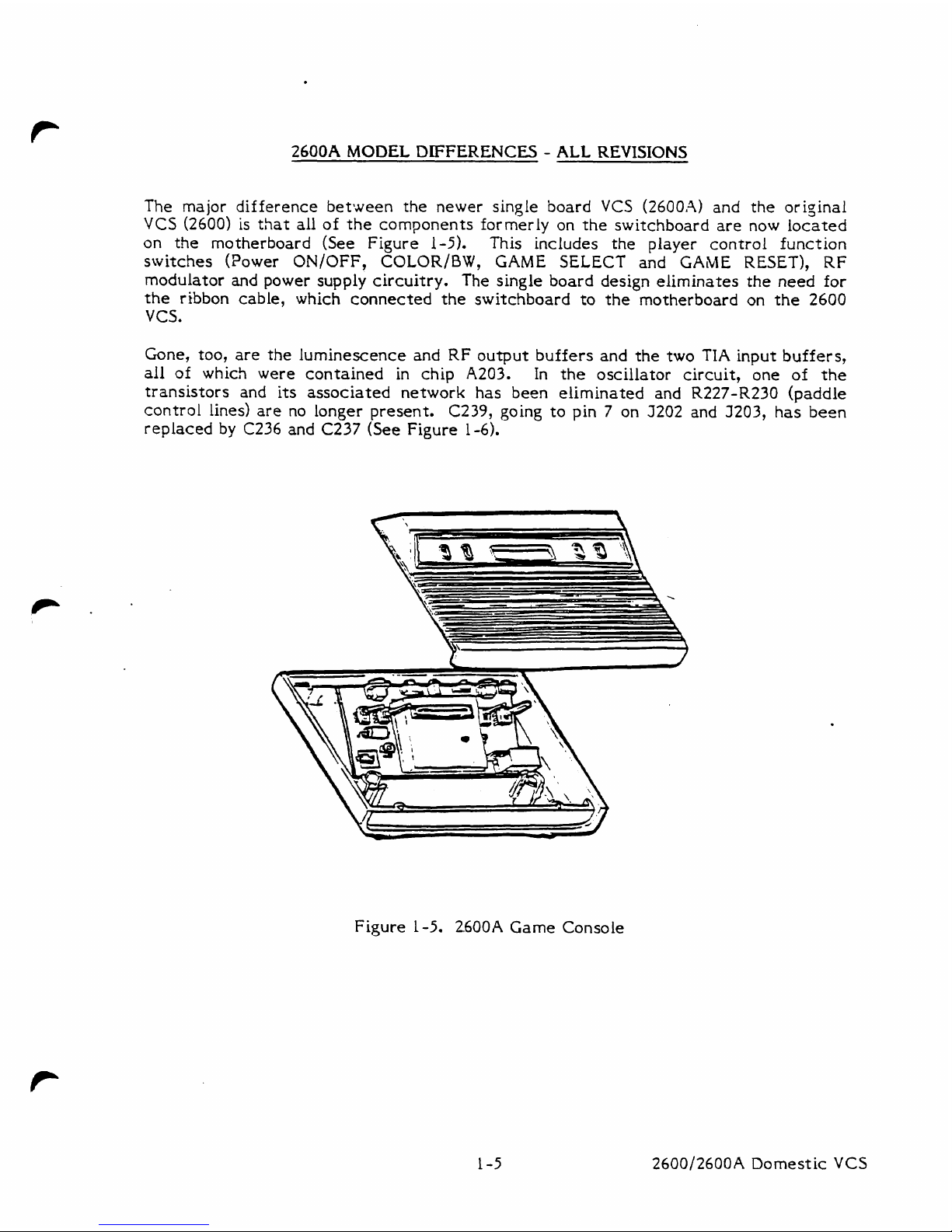
The major difference between the newer single board
VCS
(2600A)
and the original
VCS
(2600) is that all of the components formerly on the switchboard are now located
on the motherboard
(See
Figure
1-5).
This includes
the
player control function
switches (Power
ON/OFF,
COLOR/BW,
GAME
SELECT and
GAME
RESET),
RF
modulator and power supply circuitry. The single board design eliminates
the
need
for
the ribbon cable,
which connected the switchboard to the motherboard on the 2600
VCS.
Gone, too, are the luminescence
and
RF
output buffers and the two
TIA
input buffers,
all
of
which were contained in chip A203.
In
the
oscillator circuit, one of the
transistors and its associated network has been eliminated and R227-R230 (paddle
control lines)
are
no longer present. C239, going to pin 7 on J202 and 3203, has been
replaced by C236
and
C237 (See Figure
1-6).
Figure
1-5.
2600A Game Console
2600/2600A
Domestic
VCS
Page 14
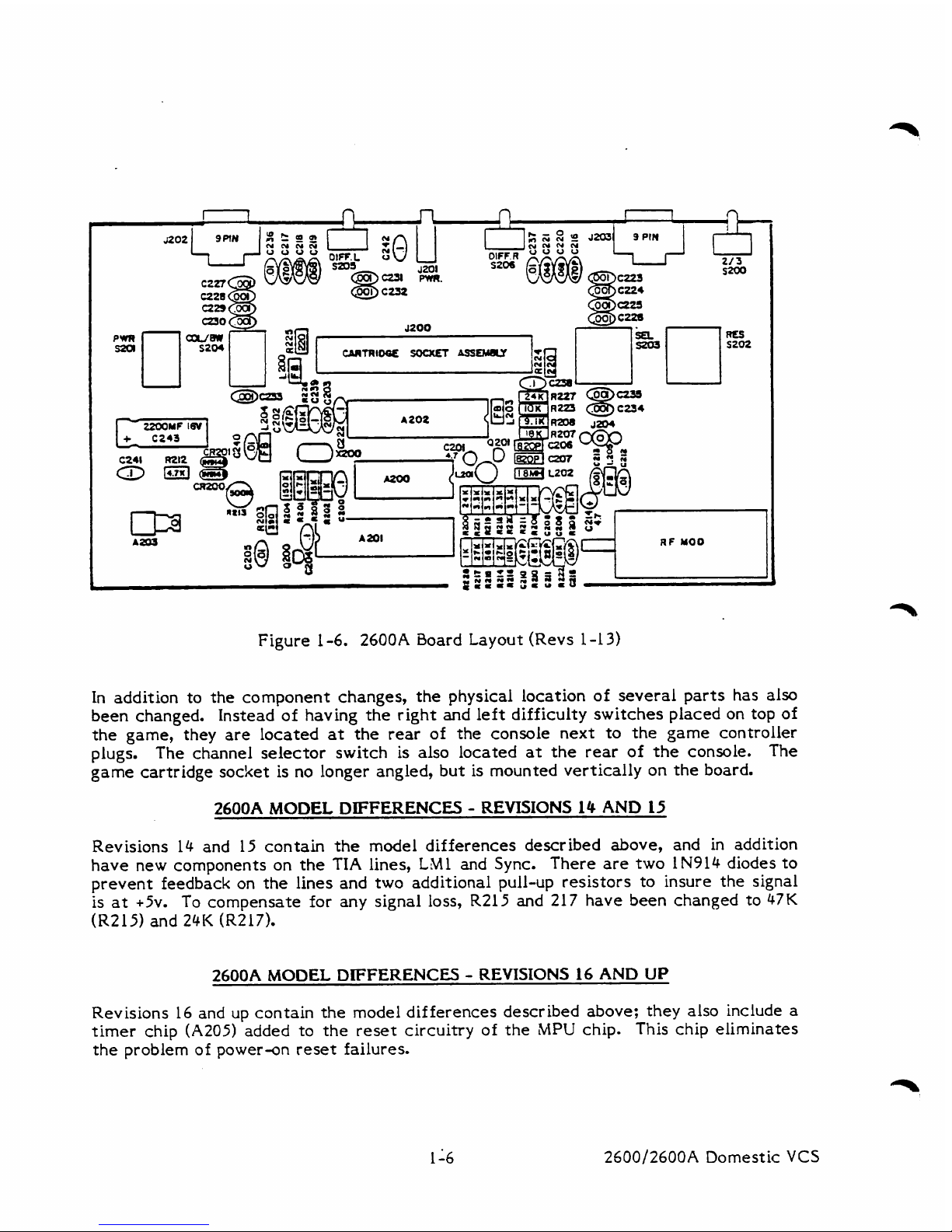
Figure 1-6. 2600A Board Layout (Revs 1-13)
In
addition to the component changes, the physical location
of
several parts has also
been changed. Instead of having the right and left difficulty switches placed on top of
the game, they are located
at
the rear of the console next to the game controller
plugs.
The channel selector switch is also located
at
the rear of the console.
The
game
cartridge socket is no longer angled, but is mounted vertically on the board.
2600A
MODEL
DIFFERENCES
-
REVISIONS
14
AND
15
Revisions 14 and 15 contain the model differences described above, and in addition
have new components on the TIA lines, LM1 and
Sync.
There are two IN914 diodes to
prevent feedback on the lines and two additional pull-up resistors to insure the signal
is at
+5v.
To
compensate for any signal loss, R215 and 217 have been changed to 47K
(R215) and
24K
(R217).
2600A
MODEL
DIFFERENCES
-
REVISIONS
14
AND
UP
Revisions 16 and up contain
the
model differences described above; they also include
a
timer
chip
(A205)
added to the reset circuitry of the
MPU
chip. This chip eliminates
the problem of power-on reset failures.
2600/2600A Domestic
VCS
Page 15

SUMMARY
The
VCS
is a microcomputer that receives its operational instructions from same
cartridges, the game console, and player controllers. The
2600
switchboard and
motherboard assemblies are housed within
an
outer casting and are the principle
assemblies addressed in
the
remainder of this manual. The boards are connected by
a
12-conductor ribbon cable which passes not only power, but
also
data between the two
boards.
Three chips of the notherboard allow for the interaction between the game
and
the
player.
These
chips are the microprocessor
(MPU),
the Random Access Memory-
Input/Output
(RAM
I/O), and
the
Television Interface Adapter
(TIA)
chips.
The
2600A
model differs primarily
in
the location of
the
components formerly located
on the switchboard. They are attached directly to
the
motherboard and eliminate the
need for the switchboard
and
the
ribbon cable. The
2600A
Revisions
14
and
up
include
even
further additional components to improve the performance
of
the output
circuitry.
2600/2600A
Domestic
VCS
Page 16

SECTION
2
SILKSCREENS
AND
SCHEMATICS
On the following
pages
are
representative silkscreens and switchboard
schematics
for
the
ATARI
Video Computer System.
The
motherboard schematics for
all
2600/2600A
VCS
models are located
in
the
pocket
at
the
front
of
this binder. Minor variations in
design
may
be encountered depending
on
the
production
date
of
the
game,
but
these
schematics provide
all
details required
for
an in-depth understanding
of
all
2600
units,
including the various
2600
A
model
revisions..
2600/2600A Domestic
VCS
Page 17

NAT.
L.kt3kO
T.I.
78MC5C
VOLTAGE
REGULATOR
(Tap
View)
A203
(Top
View)
win
version
(Channel
2
or
3)
RF
Moduiator
RF
Mod.
(TOO
View)
Figure
2-1.
2600/2600A
IC
Pinouts
2600/2600A
Domestic
VCS
Page 18

Figure
2-2.
2600
Motherboard
Silkscreen
2600/2600A
Domestic
VCS
Page 19

The
following
variations
may
appear
on
the
2600
switchboard:
CHANNEL
3
SWITCHBOARD:
C102
may
or
may
not
be
in
place.
C103
and/or
C104
may
or
may
not
be in
place.
C103
and/or
ClO4
may
be
mylar
dipped
.22
uf.
C103
and/or
ClO4
may
be
ceramic
.Oluf
(See
Figures
2-3
and
2-4).
CHANNEL
2
OR
3
SWITCHBOARD:
The
holes
on
the
PC
board
for
the
CAME
RESET
and
GAME
SELECT
switches may
not
be
wide
enough
apart for
the
switch
legs.
To
correct
this
the
legs of
the
switch
must
be
bent in
so
they
fit
into
the
holes
(See
Figures
2-5
and
2-6).
2600/2600A
Domestic
VCS
Page 20

Figure
2-3.
2600
Channel 3 Switchboard
Silkscreen
2600/2600A
Domestic VCS
Page 21

Figure
2-4.
2600
Channel
3
Switchboard
Schematic
2600/2600A
Domestic
VCS
Page 22

Figure
2-5.
2600 Channel
2-3 Switchboard Silkscreen
2600/2600A
Domestic
VCS
Page 23

Page 24

Page 25

Figure
2-8.
2600A
Motherboard
Silkscreen
(Revs.
14
and
15)
2-1
1
2600/2600A
Domestic
VCS
Page 26

Figure
2-9.
2600A
Motherboard Silkscreen (Revs.
16
and
up)
2600/2600A
Domestic
VCS
Page 27

SECTION
3
TESTING
AND
TROUBLESHOOTING
EQUIPMENT
REQUIREMENTS
You require eight basic pieces of equipment in order to analyze failures in the
2600/2600A Video Computer Systems (VCS). These items include:
A
15
MHz
oscilloscope
A
Video Computer System switchboard assembly that is known
to
be
operating properly (not required for repairing
2600A
units)
A
Video Computer System diagnostic test cartridge, version 2.6 (DTC)
Two blue controller port shorting plugs for use with the
2.6
(DTC)
diagnostic cartr
idge
Signal Tracins Cartr idqe (STC or
KLUGE)
VCS Field Service Manual for Domestic Model 2600/2600A
Color television set (properly adjusted)
Frequency Counter
2600/2600A
Domesric
VCS
Page 28
TEST
PROCEDURES
AND
METHODS
Atari requires each 2600/2600A model returned for service to be
checked
for
certain
conditions.
In some instances,
a
unit must
be
modified to conform to Atari standards.
These changes are summarized below.
2600
MODEL
MODIFICATIONS
0
Each
2600
model opened must be modified
as
shown in Figure
3-1
to
provide additional protection from static discharge..
A
Zener diode is
connected between the trigger lines and ground, and static strips are
placed on the switches on the switchboard (See Figures
3-1,
3-2
and
3-41.
These modifications are crucial to prevent component damage due to static
discharge.
Each connector and plug should be checked for
a
tight, secure fit.
Intermittent failures frequently result from a loose connector or plug.
Connectors
3202
and
3203
should
be
checked for pushed or broken pins.
If the unit has
a
green 3200 connector, insert cartridge and wiggle it.
If
the unit shows intermittent problems, replace
5200.
Each board with Ltlolex chip sockets with insertion aids should have the
insertion aids removed and the chip reinserted.
Check that all components (especially those on the
p&imetei of the
motherboard)
are
properly soldered. Check for broken or shorted trace
lines.
Check for an inductor and capacitor over
C201
and
R206. Cut the inductor
and
cap
out,
being careful not to cut the C201 or
R206
leads.
If
unit has a standup regulator and heatsink, inspect for hairline fractures
between the regulator and switchboard. Also ensure that the regulator is
firmly secured to
the
heatsink by a Tinnerman clip or rivet.
Ensure that motherboards (Rev.
8
or lower) have a colored dot over the
trace on the upper-left corner of the board. This prevents shortinq the
board and the casting (See Figure
3-3).
Two
types of 12-conductor cable assemblies
have
been
used
on
2600
model
units, the flat-wire type and the ribbon type.
When
a
defect is found in the
flat-wire type cable assembly or its male connector on the switchboard,
the flat-wire cable assembly should
be
replaced with the ribbon cable
assembly and the 12-pin male switchboard connector should be replaced
with the 1Gin female switchboard socket.
2600/2600A
Domestic
VCS
Page 29
Figure
3-1.
2600 Trigger Circuitry with Static Modification
Install the static modification on all
2600
units.
Install CR202 nd
CR203
by
removing C236 and
C237
and inserting
the
C2361CR202
and
C2371CR203
assemblies
in
their place (See Figure 3-2).
CAUTION:
Observe the polarity
on
CRZ02 and CR203 (the dark band must be toward
the 3202/3203 connectors).
On
the switchboard, install the static strips
as
shown in
Figure
3-4.
2600/2600A Domestic
VCS
Page 30

Page 31

Figure
3-4.
2600
Switchboard Static Modification
2600/2600A
Domestic
VCS
Page 32
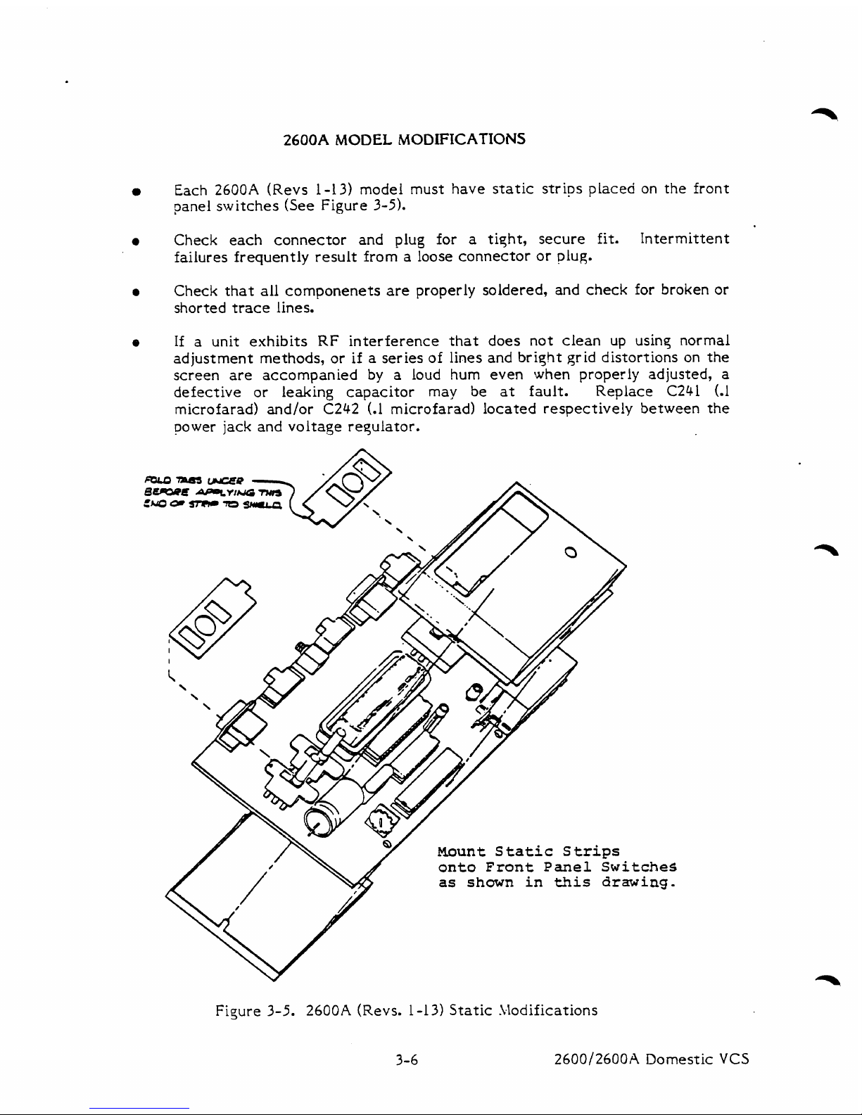
2600A
MODEL
MODIFICATIONS
Each
2600A
(Revs
1-1
3) model must have static strips placed on the front
panel switches (See Figure 3-51.
a
Check
each
connector and plug for a tiqht, secure fit. Intermittent
failures frequently result from a loose connector or plug.
a
Check that all cornponenets
are
properly soldered, and check for broken or
shorted
trace
lines.
e
If a unit exhibits
RF
interference that does not clean up using normal
adjustment methods, or if a series of lines and bright qr id distortions on the
screen
are
accompanied by a loud hum even when properly adjusted,
a
defective or leaking capacitor may
be
at fault. Replace C24l (.I
microfarad) and/or C242
(-1
microfarad) located respectively between the
power jack and voltage requlator.
ing
.
Figure 3-5.
2600A
(Revs.
1-13] Static Slodifications
3-6
2600/2600A
Domestic
VCS
Page 33
TESTING
WITH
THE
DIAGNOSTIC
TEST
CARTRIDGE
(VERSION
2.6)
The
2600
Diaqostic Test Cartridge (version
2.6
DTC) contains a varietv
of
tests
to
assist the service technician in identifying the source of problems within
the
VCS
switchboard and motherboard hardware. The
test
cartridge is used in conjunction with
the equipment listed at the beginning
of
this section. Each
test
is reviewed in the
remainder of this section. Detailed procedures for use of the tests are described in
Section
4,
2600
Diagnostic Flowchart, and Section
6,
2600A
Diagnostic Flowchart.
The
tests
available in the cartridge are:
a
RAhi
Test
Color Bar Test
a
GrayBarTest
Diagnostic Matrix Test
a
Audio Tones Test
Paddle Control Lines Test
The
technician also has a Signal Trace Cartridge
(STC
or
KLUGE)
available for
tracking motherboard problems that are not repairable with
the
Diagnostic Test
Cartridge.
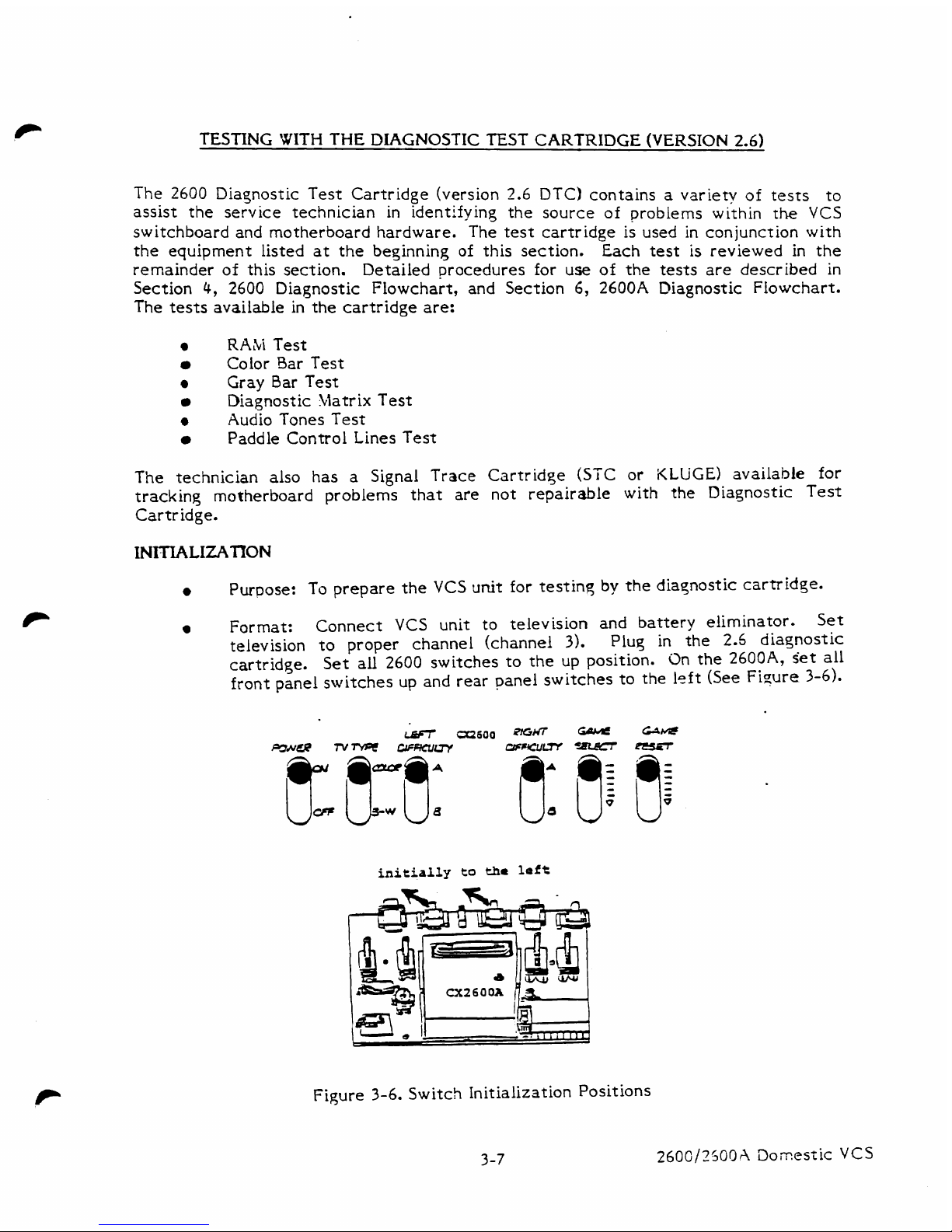
a
Purpose:
To
prepare the
VCS
unit
for
testinq
by
the diagnostic cartridge.
a
Format: Connect
VCS
unit to television and battery eliminator. Set
television to proper channel (channel
3).
Plug in the
2.6
diagnostic
cartridge.
Set
all
2600
switches to the up position.
On
the
2600A,
set
all
front panel switches up and rear panel switches to the left (See Figure
3-6).
initially
to
the
left
Figure
3-6.
Switch Initialization Positions
3-7
260G/2500A
Domestic
VCS
Page 34
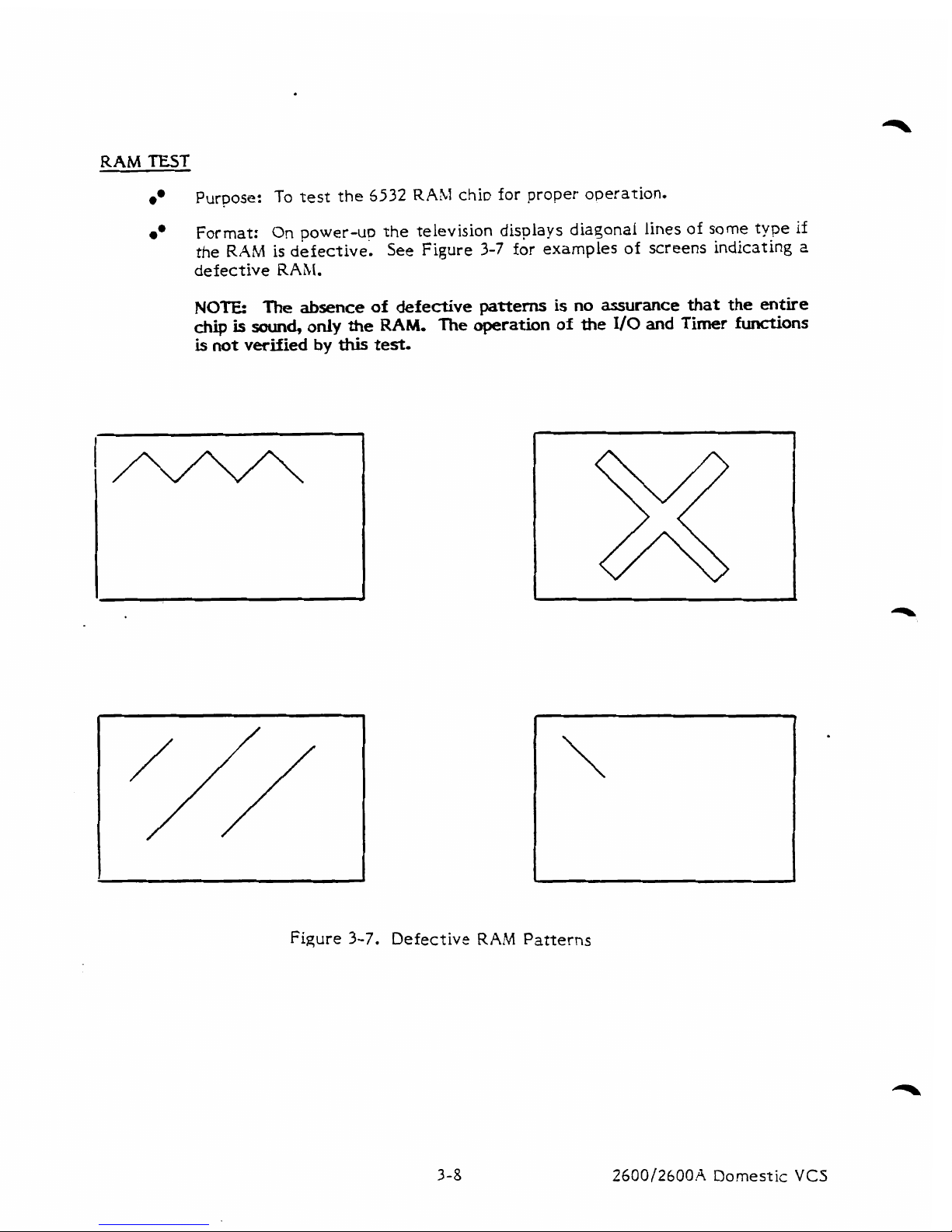
RAM
mT
Purpose: To test the
6532
RAM
chi0
for
proper
operation.
Format:
On
power-up
the
television displays diagonal lines
of
some
type
if
the
RAM
is
defective. See
Figure
3-7
for examples
of
screens indicating
2
defective
RAM.
NOTE:
The
absence
of
defective
patterns
is
no
assurance
that
the
entire
chi.
is
sound,
only
the
RAM.
The
operation
of
the
I/O
and
Timer
functions
is
not
verified
by
this
test.
Figure
3-7.
Defective
RAM
Patterns
2600/2600A
Domestic
VCS
Page 35
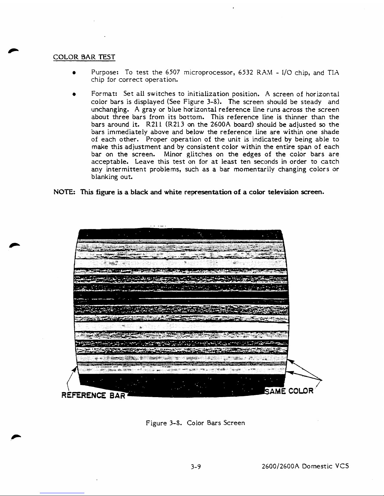
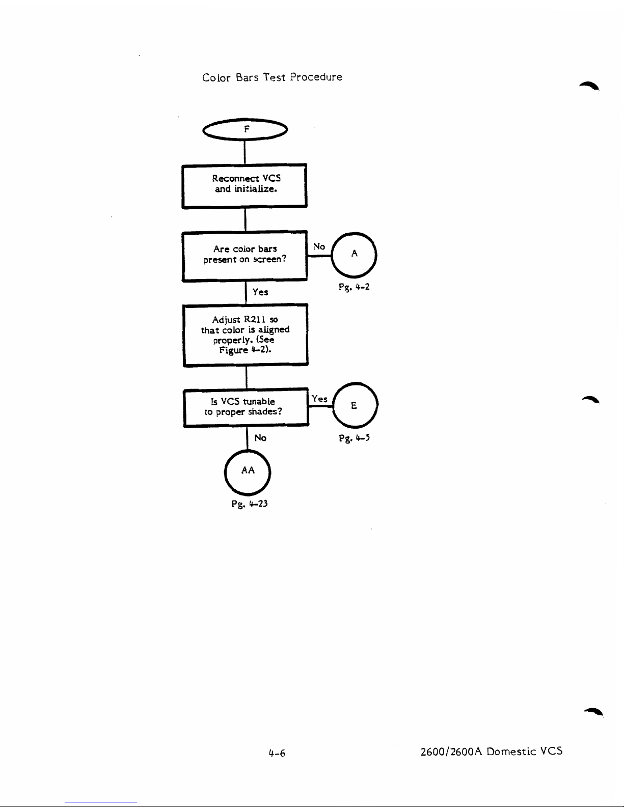
COLOR
BAR
TEST
Purpose: To
test
the
6507
microprocessor,
6532
RAM
-
1/0
chip,
and
TIA
chip for correct operation.
a
Format: Set all switches to initialization position. A screen of horizontal
color bars is displayed (See Figure
3-81.
The screen should be steady
and
unchanging.
A
gray
or blue horizontal reference line runs across
the
screen
about three bars from its bottom. This reference line is thinner than the
bars around it.
R211
(R213
on the 2600A board) should be adjusted
so
the
bars immediately above and below the reference line are within one
shade
of each other. Proper operation of the unit
is
indicated
by
being able to
make
this adjustment and
by
consistent color within the entire span of each
bar on the screen. Minor glitches on
the
edges of the color bars are
acceptable.
Leave
this test on for
at
least ten seconds in order to catch
any
intermittent problems, such
as
a
bar momentarily changing colors or
blanking out.
NOTE:
This
figure
is
a
black
and
white
representation
of
a
color
television
screen.
Figure
3-8.
Color Bars Screen
2600/2600A
Domestic
VCS
Page 36
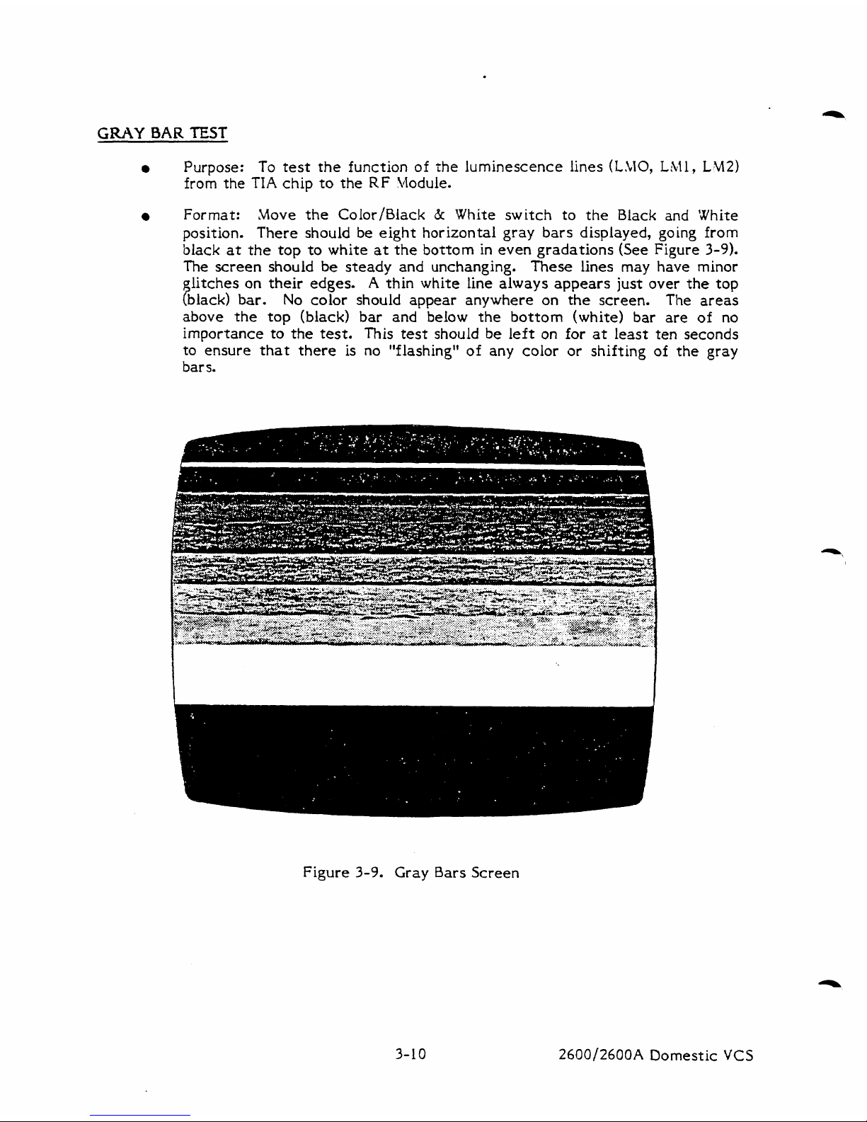
GRAY
BAR
TEST
Purpose:
from
the
Format:
position.
black
at
To
test
the
function
of
?he
luminescence lines
(LLIO,
LW,
LV2)
TIA
chip to the
RF
Module.
Move the Color/Black
&
White switch to the Black and 'White
There should be eight horizontal gray bars displayed, going from
the top to white at the bottom in even gradations (See Figure
3-9).
The screen should
be
steady and unchanging.
fhese
lines
may
have
minor
litches on their edges.
A
thin white line always appears just over
the
top
black)
bar.
No color should appear anywhere on the screen. The
areas
S
above the top (black) bar and below the bottom (white) bar are of no
importance
to
the
test.
This
test
should be left
on
for
at
least ten seconds
to ensure that there is no "flashing"
of
any
color or shifting
of
the gray
bars.
Figure
3-9.
Gray
Bars Screen
2600/2600A
Domestic VCS
Page 37
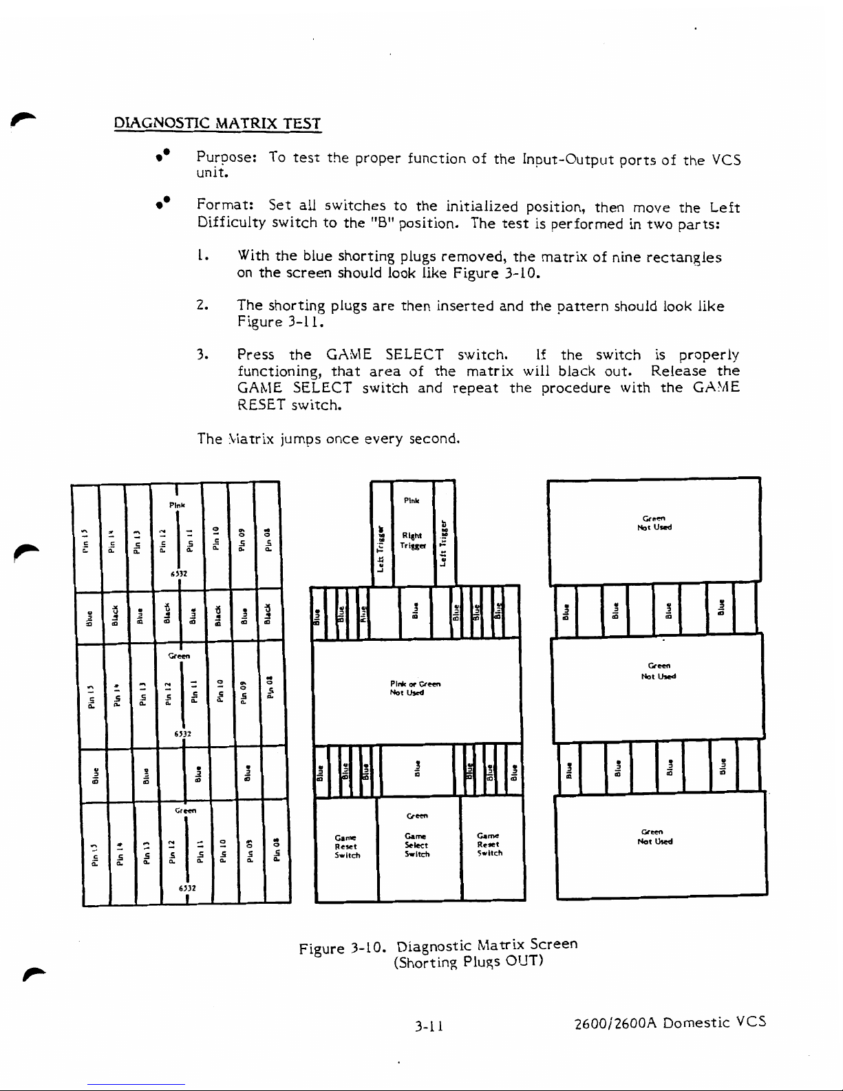
DIAGNOSTIC
MATRIX
TEST
Puroose: To test the proper function of the Input-Output ports of the
VCS
unit.
Format: Set all switches to the initialized position, then move the Left
Difficulty switch to the
"8"
position.
The
test
is performed in two parts:
1.
With the blue shorting plugs removed, the matrix of nine rectangles
on the screen should look like Figure
3-10.
2.
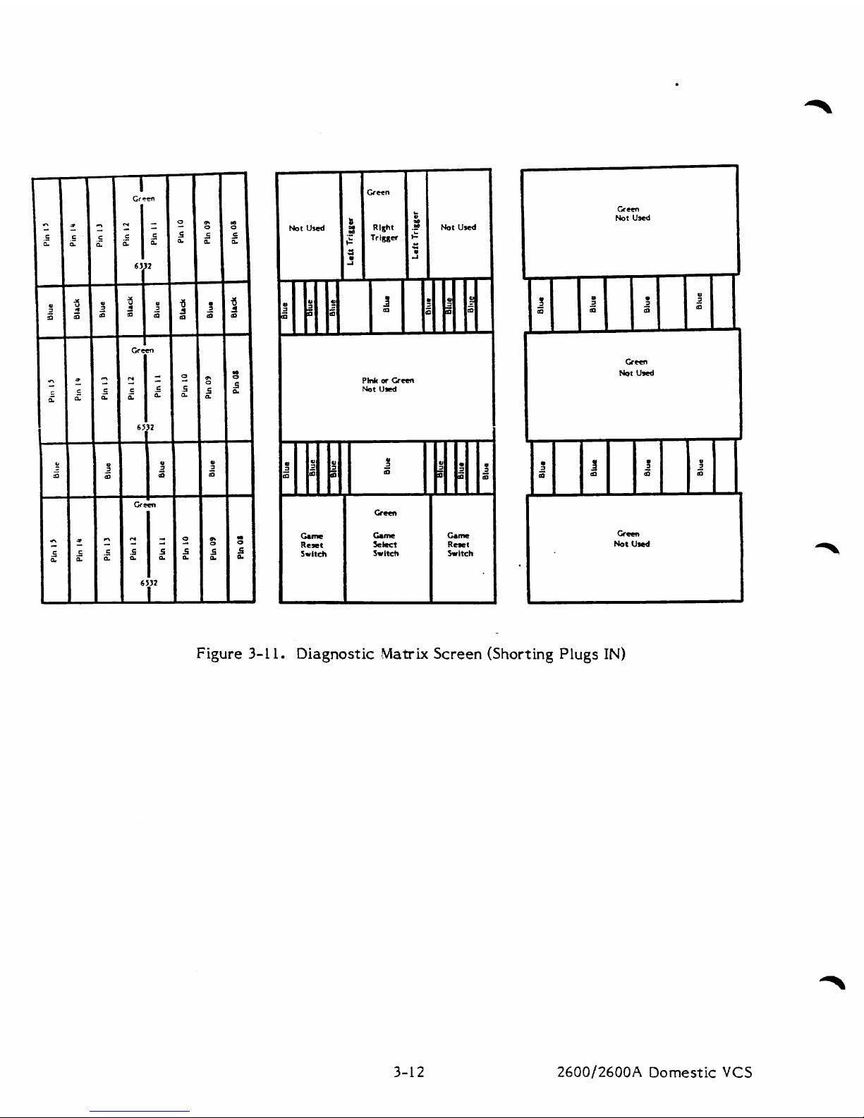
The shorting plugs are
then
inserted and the pattern should look like
Figure
3-1
1.
3.
Press
the
CAME
SELECT
switch. If the switch is properly
functionins, that area sf the matrix will black out. Release the
GAME
SELECT
switch and repeat the
RESET
switch.
The Ciatrix jumps once every second.
procedure with the
GAVE
Plnk
a
Green
Not
used
Came
kkct
hitch
a,
;o'
CIma
Rc¶et
Svltch
Gr
un
Not
Und
Figure
3-1
0.
Diagnostic Matrix Screen
(Shorting Plugs
OUT)
2600/2600A
Domestic
VCS
Page 38
Pink
a
Gmr
Not
Urd
Gama
Rmt
hrltch
Gem
Not
UYed
Figure
3-1
1.
Diagnostic
Matrix
Screen
(Shorting
Plugs
IN)
2600/2600A
Domestic
VCS
Page 39
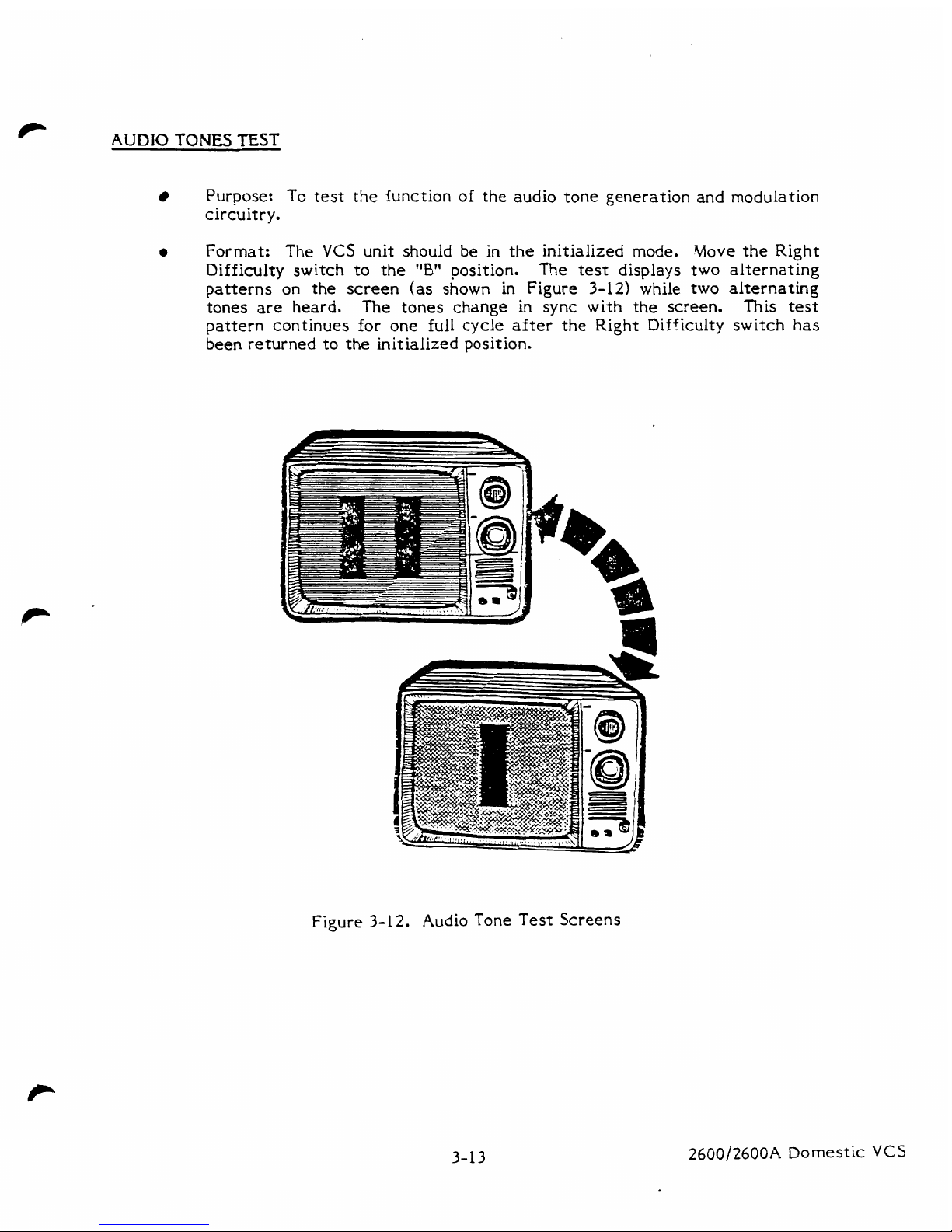
AUDIO
TONES
TEST
Purpose:
To
test
the function
of
the audio tone generation and modulation
circuitry.
0
Format: The
VCS
unit should
be
in the initialized mode. Move the Right
Difficulty switch to the
"8"
position.
The
test
displays two alternating
patterns on the screen (as shown in Figure
3-12)
while two alternating
tones are heard.
The
tones change in sync with the screen. This
test
pattern continues
for
one full
cycle
after the
Right
Difficulty switch
has
been returned to the initialized position.
Figure
3-12.
Audio Tone Test Screens
2600/2600A
Domestic
VCS
Page 40
PADDLE
CONTROL
LINES
TEST
-
-
a
Purpose:
To
test the proper operation
of
the Paddle Control
Lines
by
viewing
the
analog waveforms
at
the analog-to-digital conversion inputs
of
the
TIA
chip.
Format:
Pins
37,
38, 39,
and
40
of the
TIA
chip
are
checked
with the
oscilloscope with the
VCS
unit
in
Diagnostic Matrix mode and with the
shorting plugs
in
place. This
test
is required only if there
is
a
problem
with
the
hand
controller lines. The procedure for
this
test
is detailed
in
Section
4.
2600/2600A
Domestic
VCS
Page 41
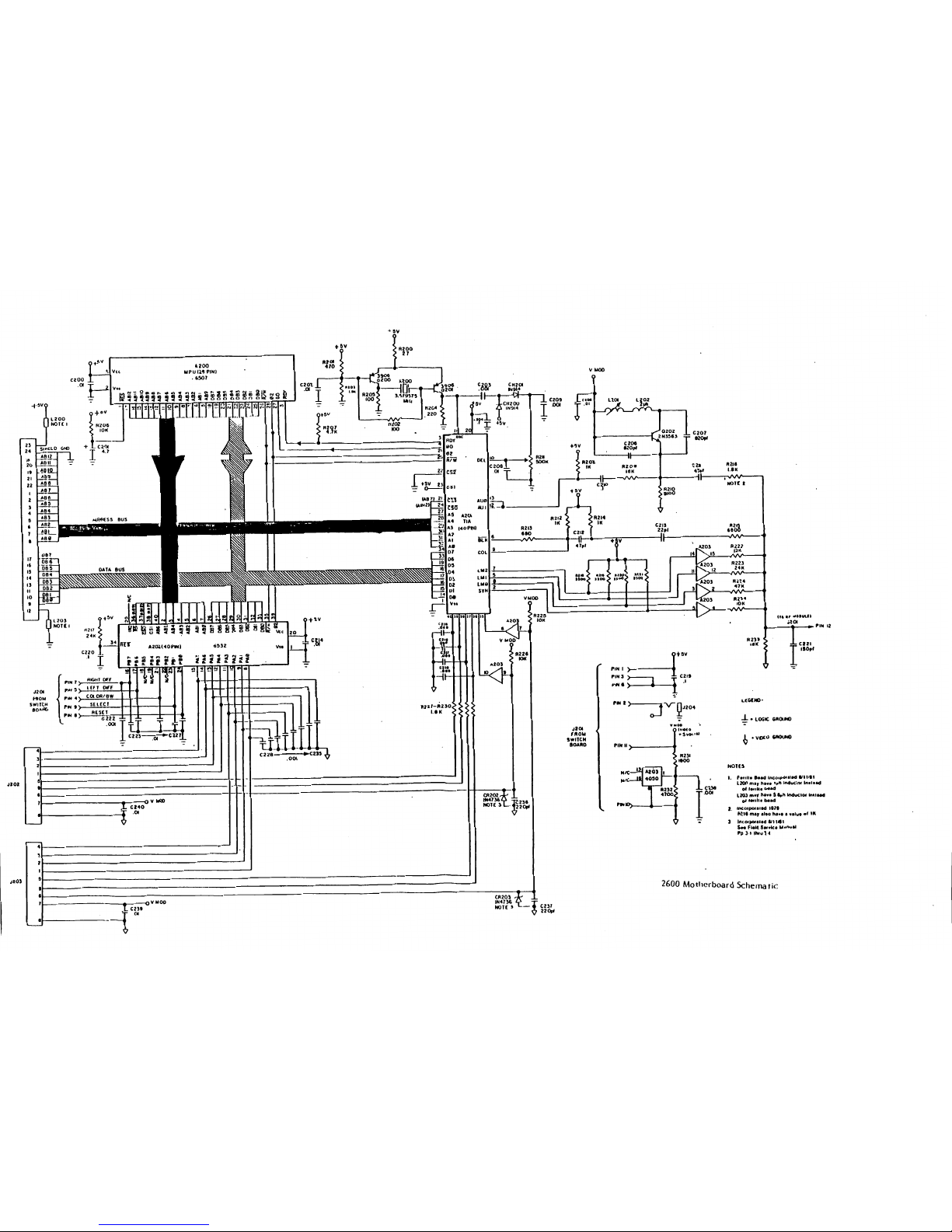
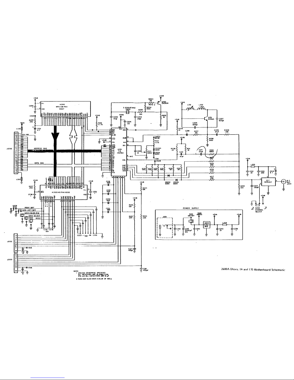
42a
Tlh
4040
COL
2600
Motherboard
Schematic
Page 42

Page 43
Page 44

SECTION
4
2600
DIAGNOSTIC
FLOWCHART
The Diagnostic Flowchart is intended to be easy to use and the primary aid when
troubleshooting the 2600.
Follow the prompts in the order presented. When
a
quesrion
is asked, follow the line from that box which best applies to the unit's condition. The
figures referenced
in
the flowcharts are located
at
the end of this section. When
a
line terminates with a letter inside a circle, note that a page number (i.e., pg.
4-31
is
near it. Turn to that page, locate the letter in another circle,
and
continue the
diagnosis. The flowchart leaves nothing to chance, it tells you when to perform a
specific test, and when to replace components, and even when and how long to "burn-
in"
the unit. "Burn-in" the unit for
at
least two hours after completing repairs.
When a problem is extremely difficult to diagnose, the flowchart sends you
to
the
Signal Tracing Cartridge (STC) routine,
"D"
page 4-47. Due to the repetitive nature of
the STC routine, no flowchart is used.
Read and follow the instructions
as
directed.
Should the STC procedure fail to isolate the problem, after carefully inspecting the
switchboard and motherboard assemblies for shorted and/or open trace lines, and
solder
bridges swap all three chips (6507, 6532, and
TIA).
Should the problem still
persist, call
ATARI,
Techline Specialist: Inside California at (800) 672-1466
and
Outside California
at
(800) 538-1535.
Be
certain to always burn-in the unit for two
hours after completing repairs. This helps to ensure that intermittent problems are
found and also greatly increases your customer's satisfaction with your repair work.
SWAP
OUT
PROCEDURES
Many
places in the diagnostic flowchart, a box tells you to "swapout" a chip or
a
number of chips in
a
order.
The "swapout" instruction means that you
should replace the indicated components one
at
a time with a known sood component
of
the same type. The
VCS
should then be tested with the new, known-good
component in place to see whether the "swapout" solved the problem being checked.
If
the swapout did not fix the problem, the known-good component should be left in, and
the next component inserted. Once the problem is solved, you then place the
suspected
bad
chips one by one into the system to determine whether or not those you
pulled out are truly defective.
In
this way, you avoid needlessly replacine, gbod
components.
CAUTION
- - -
-
-
-
-
-
Extreme
care
should
be
taken
when handling
the
integrated circuit
chips
(A200,
A20
1,
AZ02,
A203).
They
are
all
very sensitive to
static
electricity
and
can
easily
be
damaged
by
careless
handling.
Always
keep
the
chips
in
their
plastic
carrier
tubes
or
on conductive foam
when
not
handling
them.
Make
certain
you are
well
grounded
when
handling
the
chips.
Atari
strongly
recommends that
you
wear a conductive
grounding
band
(which ties from
your
arm
to
ground) when handling
the
chips.
The
chips
are
also
susceptible
to
damage
from
stress
when
being
removed
from
or
inserted
into
the
sockets
Always
use
a
chippuller
when
removing
the
chips.
Do
not
pry
chips
out
with
a
screwdriver or
any
other
tool.
Failure
to follow
the
above
guidelines
results
in
unusually
high
chip failure
rates
and
extra
expense.
'
2600/2600A Domestic
VCE
Page 45

2600
Diagnostic Flowchart
Connect
VCS
to
N
barmy
elimi-
nator.
Set
TV
to
I
Insert
Diagnostic
Catnidge
(DTC),
in-
it-
(Figure
4-11
and
aPn
on.
I
I
I
bCS
MY
fective
RAM
k
picave
No
warped
and
ragged
P.m
apQear
-
on
left
side
muse#r(sec
Fig.
4-31.
of
m?
Replace
the
A202
I
2600/2600A
Domestic
VCS
I
-
9howtfitcobr
bars
panern?
Does
unit
now
~IOW
the;
No
cobr
bus
panem?
A
Y
5w-
I)
Am
2)
A202
Page 46

2600
Diagnostic
Flowchart
(Continued)
i
Are color bars
P
Are
color
bars
2
Yes
present?
Yes
properly
adjusted?
r
'See
Figure 4-21.
(See Figure 4-2)
I
No
b
J
No
1
m
I
4
Is
any
other
test
Check
your
No
pattern on the
,Yes
switch
settings.
screen?
I
J
Are they correct?
w
(See Figure 4-4,
4-694-9)-
I
A
a
w
Pg.
4-7
Is
there "snow" No
Is
ANY
on
the
screw?
modulation
(no modulation) ~resent on screen? No
1
I
Check
VCS
1
w
connections
to
TV
and
Test
VCS
with
known
-
good
battery
eliminator.
Pg.
4-9
Pg.
4-1
1
I
IS
"snow"
on
screen gone?
Pg.
4-6
Yes
2600/2600A
Domestic
VCS
Page 47

Bad
Video
Troubleshooting
procedure
KO
Bad
switchboard
identify
bad.
I
DotJ
A203
have
No
Repair
open
trace.
Yes
pod
Va
(+Sv
at
-
Das
unit
now
have
'
pin
8)
and
ground
a
picture?
(at
pin
1
I?
'
b
I
k
a
b5v
pg
signal
pmcnt
Rcpke
A203.
at
pin
S
of
A203?
pattern
an
the
N?
Cheek
R221,
Is
it
Replace
RZ21
I
OK?
(33K)
b
I
Yes
Chcck
that
the
trace
line
from
A201 pin
2
is
not
droned
1
toanother
Line.
1s a picwe
now
pmmt
on
0
Pg.
f6-4
Pg.
4-2
I
r
Yes
Yes
2600/2600A
Domestic
VCS
Is a picture
No
now
present
on
-
the
TV?
No
-
Swapout
1)
A200
2)
A202
b
a
picture
now
present
on
the
N?
h
-
Page 48
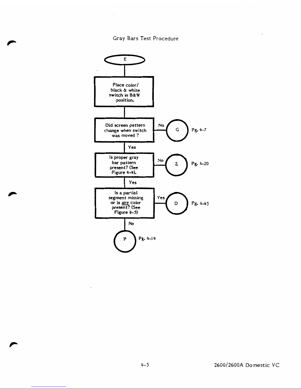
Gray
Bars
Test
Procedure
Place
color/
black
&
white
switch
in
BhW
.
posit
ion.
Did
screen
pattern
change when
switch
was
moved
?
Is
proper gray
bar
pattern
present?
(See
Figure
4-4).
Pg.
4-7
Is
a
partial
segment
missing
or
is
any
color
pg.
4-45
present?
(See
Figure
4-51
2600/2600A
Domestic
VC
Page 49
Color
Bars
Test
Procedure
and
initialhe.
u
I
Are
color
bars
mesent
on
screen?
Pq*
4-2
Ad
just
R211
SO
that
color
is
aligned
properly.
(See
Figure
4-21.
I
Is
VCS
tunable
to
proper
shades?
Pg.
4-23
-
2600/2600A
Domestic
VCS
Page 50
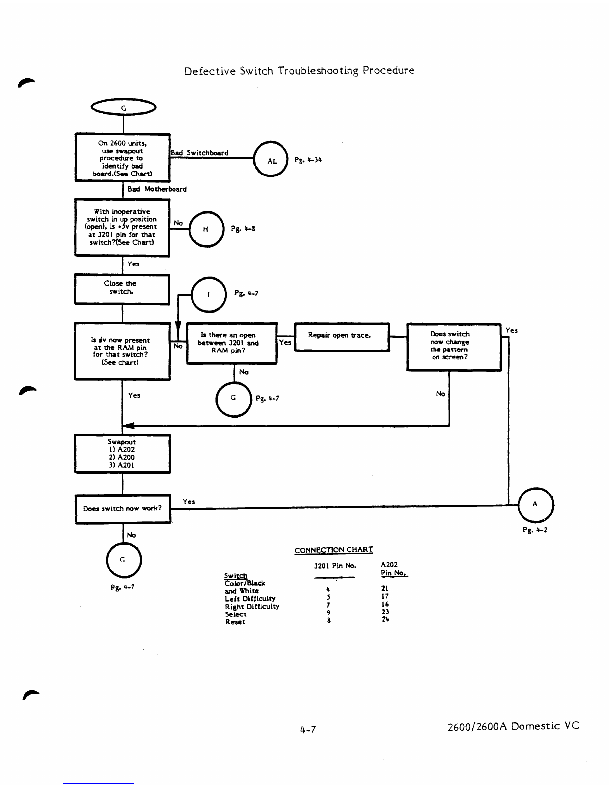
Defective
Switch
Troubleshooting
Procedure
With
inqxrative
switcb
,in
position
(open).
u
+Y:
prnmt
at
3201
pin
for
that
switch?(See
Chart)
bdvnotwpresent
at
the
RAM
pin
for
that
switch?
(see
chart)
Yes
h
there
an
open
-
Repair
open
trace.
-
Does switch
Yes
No
ktareen
1201
and
Yes
now
chnge
RAM
pin?
~rm
on
screen?
b
No
I
b
Yes
fhes
~witCfi
now
work?
I
i
Pg.
4-7
and
White
Lait
Difficulty
Right
Difficulty
kkt
Rest
t
CONNECflON CHART
2600/2600A
Domestic
VC
Page 51
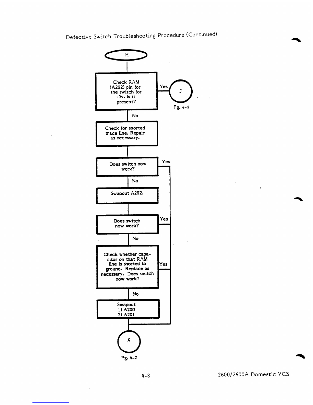
Defective
Switch
Troubleshooting Procedure
(continued)
Check
RAM
(A2021
pin
for
the
switch
for
+5v.
Is
it
present?
Pg..
4-9
Check
for
shorted
trace
Line.
Repair
as
necessary.
Does
switch
now
work?
Swapout
A202
2
Does
switch
now
work?
Chd
whether
capa-
citor
on
that
RAM
line
b
shorted
to
ground
Replace
as
necessary.
Does
switch
now
work?
Pg.
4-2
2500/2600A
Domestic
VCS
Page 52
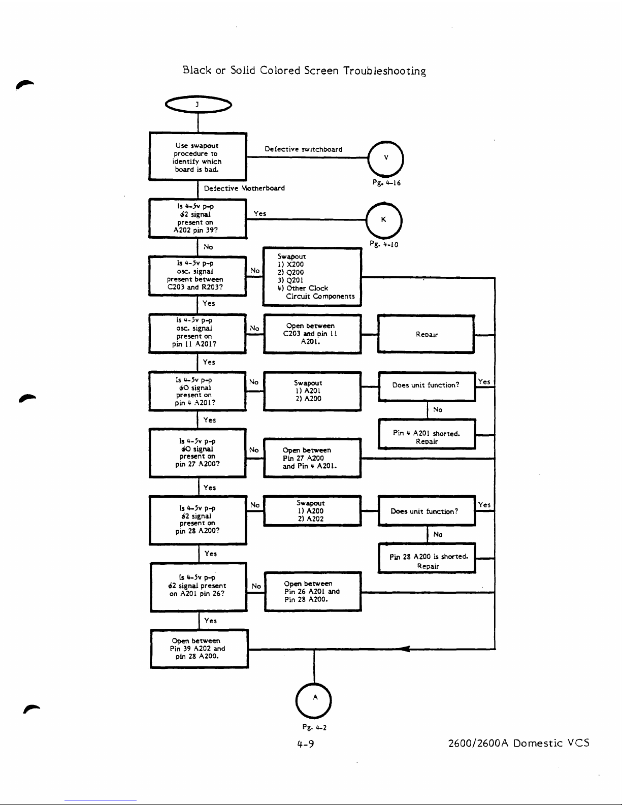
Black
or
Solid
Colored Screen
Troubleshooting
Use
swapout
procedure to
Defective switchboard
identify
which
board
is
bad.
Pg.
4-16
Defective .Motherboard
I
b
J
Is
4-E,
p-p
d2
signal
Yes
prexnt on
A202
pin
392
Is
4-5v
p-0
ox.
signal
present betureen
C203
and
R203?
Pg.
4-1
0
1)
X200
2) Q200
3) 4201
4)
Other
Clock
Circuit Components
#
I
Is
4-jv
p-p
v
b
-
ox. signai
Opm
between
prexnt
on
0
C203
and
pin
1
I
-
Reoalr
-
pin
11 .4201? A20
1.
I
Is (C-5v
p-p
dO
signal
Does
unit
function?
present on
1) A201
pin
4
A201?
2)
A200
I
L
Pin
Q
A201
shorted.
b
4-5v
p-p
b
Reoair
do
signal
No
Openbemeen
present
on
-
Pin
27 A200
I
pin
27 A200?
and
Pin
4
A20 1.
i
b
Yes
I
No Swapout
b
4-5v
p-p
Yes
-
1) A200
-
Does
unit function?
-
d2
signal
prexnt
on
2) A202
pin
28 AMO?
Pin
28 A200
is
shorted.
b
4-5"
&
b
62
signal present
N~
Open
between
on
A201
pin
26?
-
Pin
26 A201
and
Pin
28 AZOO.
L
b
I
Ooen
between
Pin
39 A202
and
pin
28
A200.
2600/2600A
Domestic
VCS
Page 53

Black
or
Solid Colored Screen Troubleshooting
(Continued)
a
I
Is
4-5v
p-p
d
.
No
Open
trace
d2
signal
I
between
pin
26
present
on.
A201
and
pin
39
pin
26 A201?
A202.
L
b
Yes
Is
there
+5v
and
No
ground
on
all
of
Open
on
line
I
I
AZOO,
A201,
A202,
to
+5
or
ground.
t
A203?
I
I
Reset
and
ready
lines
good?
Open
or
shorted
line.
t
Swapout
1)
A200
2)
A202
Does
unit
operate
Pg*
4-45
properly?
Repair
n
Pg.
4-2
2600/2600A
Domestic
VCS
Page 54
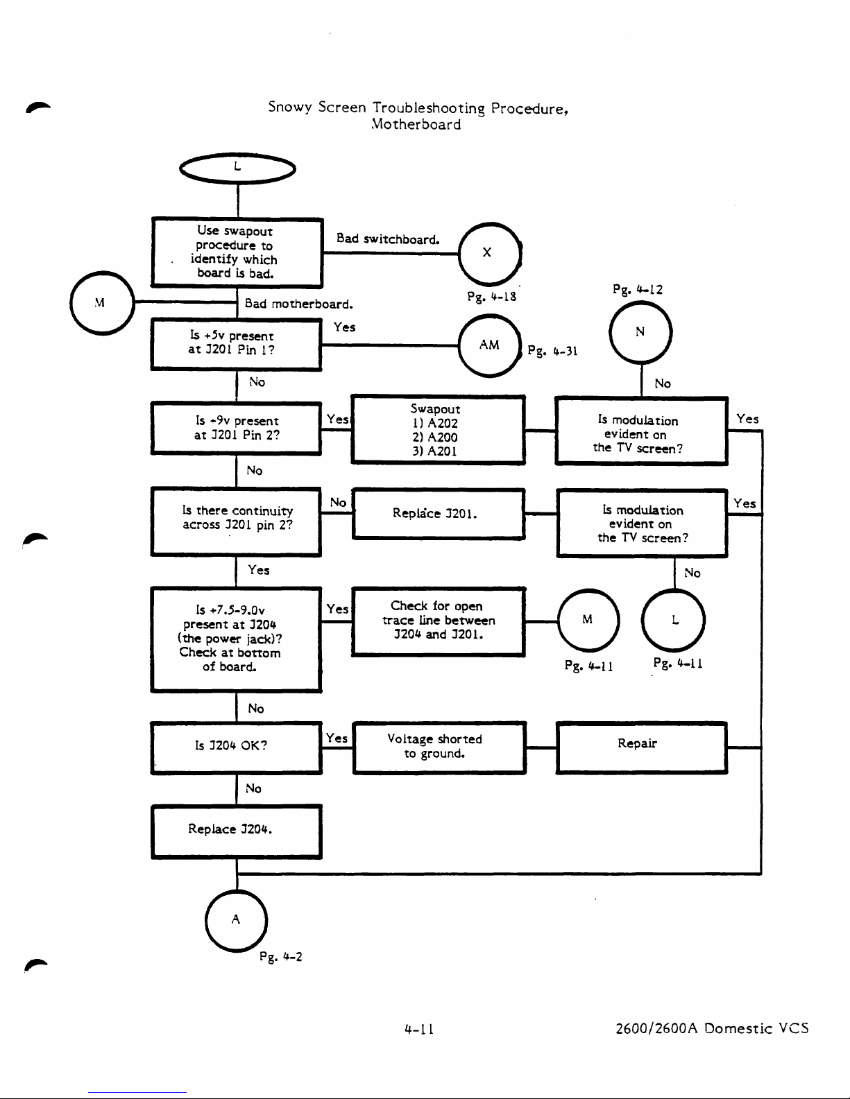
Snowy
Screen
troubleshoot in^
Procedure,
Motherboard
I
Use
swapout
Bad
switchboard.
procedure to
.
identify which
board
is
bad.
Pg.
4-18
Bad motherboard.
I
Yes
1s
+5v
present
at
J2Ol
Pin
I?
i
Pg.
4-12
L
4
J
No
Is
modulation
Yes
Is
there
continuity
Replice 520
1.
across
5201
pin
2?
evident on
the
TV
screen?
i
A
Yes
No
Is
+7.5-9.0~
present at 3204
(the
power
jack)?
Check
at
bottom
of
board
*
Replace
J204.
4
1
2600/2600A
Domestic
VCS
No
Yes
I
Is
3204
OK?
0
pg.4-ll
0
-
Pg. 4-1
1
r)
I
4
I
I
Check
for
open
trace
line
between
J204
and
J201.
7
Repair
d
I
M
t
b
Yes
Voltage
shorted
to ground.
Page 55
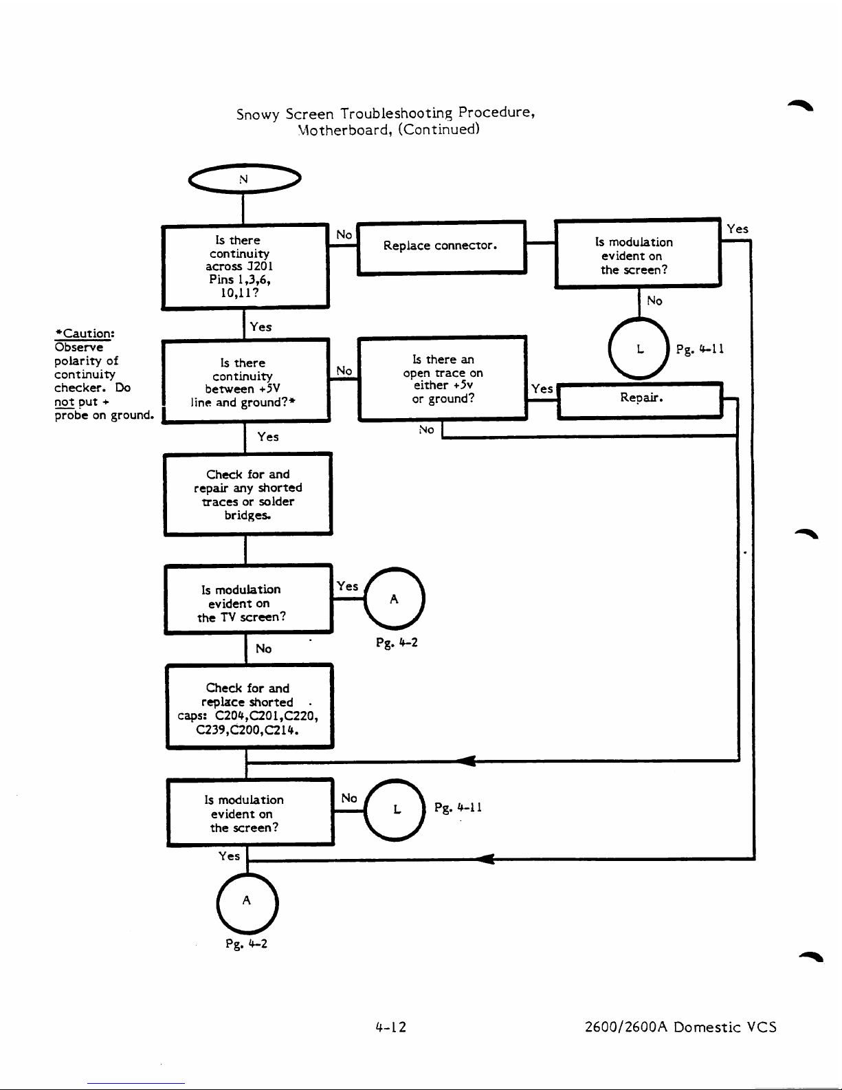
*Caution:
Observe
polarity of
continuity
checker.
Do
=put
+
probe on ground.
Snowy
Screen Troubleshooting Procedure,
Motherboard,
(Continued)
I
Is
there
W
Is
there
an
continuity open trace on
between
+5V
either
+5v
line
and ground?* or ground?
I
I
Yes
No
1
Check
for and
repair any
shorted
traces
or solder
bridges.
&
h
b
No
'
Yes
Is
there Replace connector.
,
I
Is
modulation
continuity evident on
across J201
i
the
screen?
Pins
1,3,6,
10,l
l?
Is
modulation
the
TV
screen?
Pg.
4-2
Check
for and
rtplace
shorted
.
I
caps:
~204,~01,~220,
C239,C200,CZl'l.
I
Is
modulation
evident on
the
screen?
Pg.
4-1
1
Yes
Pg.
4-2
2600/2600A
Domestic
VCS
Page 56
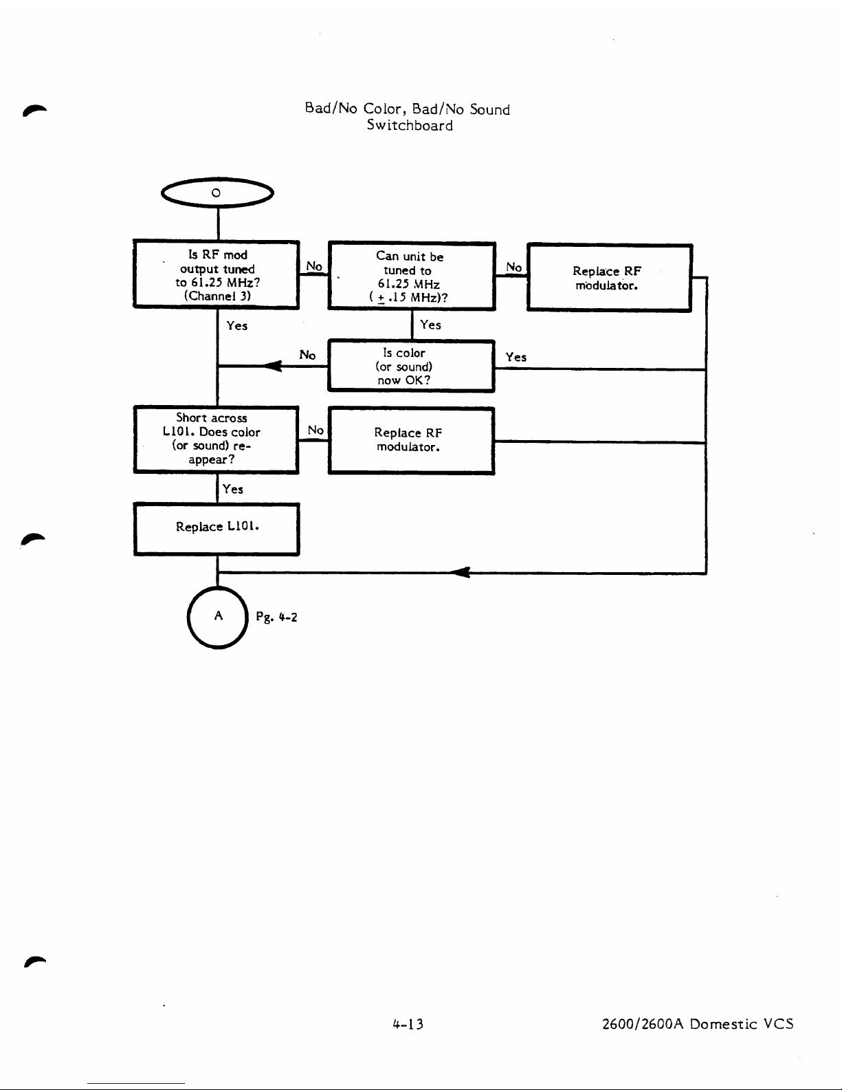
Bad/No
Color,
Bad/No
Sound
Switchboard
No
Is
color
Yes
I
(or
sound)
I
now
OK?
J
b
I
li
L
Is
RF
mod
Can
unit
be
output
tuned
No
tuned to No Replace
RF
to 61.25
MHz?
61.25
MHz
modulator.
(Channel
3)
(
2
-15
MHz)?
b
Replace
LIOL.
u
1
I
I
2600/2600A
Domestic
VCS
Yes
I
L
L
Replace
RF
modulator.
4
Short
across
L
10
I.
Does
color
(or
sound)
re-
appear?
w'
No
I
I
Page 57

Gray
Bars
Troubleshooting
Procedure
Isthere
a
3-5v
p-p
signai
on
the
A203
side
of
R222,
r
R223.R224?
I
Do
all
of
pins
2,
12,
and
15
on
A203
have
a
signai
present?
Yes
-
Yes
-
Ohm
meter.
Replace
any
failed
or
of
f-value
resistors.
Pg.
b45
There
is
an
open
line
between
A203
and
the
resistors.
Fix
it.
Pg.
4-5
I
I
m
Check
inputs
of
Yes
A203
(pins
3,11,14).
Replace
A203.
Does
each
have
a
signal
present?
1
I
Do
all
of
pins
5,7,8
on
A20
1
have
a
signal
present?
Check
for
open
'll
linesbetwen
A201
and
A203.
Fix.
I
Pg.
b15
Pg.
4-2
2600/2600A
Domestic
VCS
Page 58

Gray
Bars
Troubleshooting
Procedure
(Continued)
Make
sure
1121
8,
R219, R220
have
+Iv
connected
to
top
side.
I
Picture
Now
Yes
OK?
(See
Figure
4-4)
Check
RZl8,RZl9,
RZ2O
for
proper
Inspect
traces
around
LM
lines
for
shorts
or opens.
I
A
&
J
Go
to
matrix
test.
'and
then
A202.
I
I
Is
picture
now
OK?
(See
Figure
4-4)
L
I
J
Is
picture
now
OK?
Yes
(See
Figure
4-41
Yes
Pg.
4-20
2600/2600A
Domestic
VCS
Page 59

Colored
Screen Troubleshooting Procedure
Switchboard
Bad Switchboard
=?
Is
+5v
at JlOl
Pin
I?
Pg.
4-17
4
Is
RF
mod.
output
Tune
RF
mod.
If
RF
mod
cannot
be
tuned to
61.25
MHz
No
at
adjustment tuned
to
61.25
MHz,
(channel
3,+
.I5
hole.
replace
it.
MHz)
B
b
Is
video
signal
pre-
sent
at
JlOl
pin
12?
Check
for open
trace
or
bad
connection
be-
tween
J2Ol
and
RF
module
pin.
Repair,
Chdc
for
shorted
trace.
If
none
is
found,
the
RF
module
is
shorted
and
must
be
replaced.
I
Pg.
4-2
Is
JlOl
pin
12 shorted
to
ground?
P
2600/2600A
Domestic
VCS
I
.
No
~efective 3101.
Replace
Page 60

Colored
Screen
Troubleshooting
Procedure,
Switchboard,
(Continued)
m
Is
+9v
present
yes
)
Yes
Is
ClO
1
shorted?
L
Replace
C10
1.
at
JlOl
Pin
2?
v
t
b
Replace
voltage
I
I
regulator
(A10
1).
I
shorted
to
ground.
I
-
Check that C10
1,
C103,
or
C106
are
not shorted.
Replace
if
shorted
I
1
P
If
+9v
is
still
not present
at
JlOl
pin
2,
then rephce
the regulator
(A101).
Pg.
4-20
2600/2600A
Domestic
VCS
Page 61

Snowy
Screen
Troubleshooting
Procedure,
Switchboard
IS
+5v
present
at
3101
pin
1
on
the
switchboard?
Pg.
4-19
I
Is
+5v
at
the
RF
modulator
pin
3
(5
pin
mod)
or
pin
2
(3
pin
mod)?
RF
module
output
is
tuned
to
6
1.23
MHz.
(
2
-15
MHz).
r-=
I
t
Check
for
and
Does
RF
modulator
No
repair
opens
be-
pin
1
have
con-
RF
module
pin
1
tinuity to
ground?
and
3101
pins
6
J
L
and
10
(ground).
If
tbere
is
still
.
a
white screen,
check
the
JlO2
connector.
Replace
as
required.
A
Open
between
A10
1
pin
3
and
RF
module
pin
3-
-
If
no
modulation,
the
RF
module
is
bad.
Replace.
r
I
4
Repair
Yes
*
I
Is
there
modulation?
A
-
2600/2600A
Domestic
VCS
Page 62

Snowy Screen Troubleshooting Procedure,
Switchboard, (Continued)
I
Is
+5v
at the
output
of
the
voltage
regulator
(A101,
pin
3)?
I
Is
unregulated
47.5-9v
at voltage
regulator
input
(A101,
Pin
l)?
Check
for
bad
regulator
(AlOl)
or
open
between
ground
and
A101.
I
-7.5-9v
present
yes
RephCe
SiOl.
-
on
the
3101
side
of
I
Does"rh
2
have
continuity?
(
Yes
I
Is
JlOl
pin
2
shorted
to
ground?
l$l
Replace
5
10 1.
Check
that
C103
or
C106
have
not
shorted
to
ground.
u
itre()
Is
there
modulation?
0
Pg.
4-2
2600/2600A
Domestic
VCS
Page 63

blatr
ix
Test
Procedure
I
Initialize
switches,
the?
push
"left"
difficuity
swltCh
down.
I
Does
screen
match
Figure
4-6?
Put
in
shorting
plugs.
Does
screen
match
Figure
4-7?
Pg.
4-23
Push
down
"Game
Select"
switch
(5
106).
..
I
Did
lower
middle
block
on
screen
turn
bia&
in
center?
"Reset"
switch
(SlOS)
Does
lo
wet
middle
block
turn
black
on
left
and
right ends?
Yes
Pg.
4-7
Pg.
4-24
2600/2600A
Domestic
VCS
Page 64
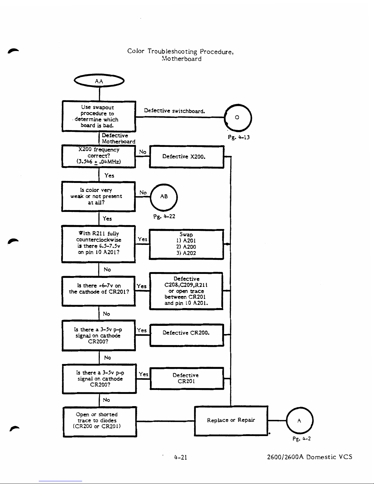
Color Troubleshooting
Procedure,
?Jo
therboard
tive switchboard.
X200 frequency
1
correct? Defective X200.
1
Yes
Is
color
very
weak
or
not
present
at
all?
1
Yes
Pg.
4-22
I
With RZll
fully
countcrciockwix
is
there
6.5-7.5~
on
pin
10 A201?
-
I
Defective
b
there
+6-7v
on
the
cathode
of CR201?
I
Defective
signal
on
cathode
CRZOO?
CR20
1
I
1s
there a 3-5v
P*
signal
on
cathode
C
Open
or
shorted
trace
to
diodes
Replace
or
Repair
(CR2OO
or
CR20
1
)
A
I
Pg.
4-2
Yes
2600/2600A
Domestic
VCS
C208,C209,RZll
or
open
trace
between
CR2Ol
8
A
P
and
pin
LO
A201.
No
I
I
-
Yes
Detective
CR200.
Page 65

Color Troubleshooting
Procedure,
Motherboard,
(Continued)
Does
screen
now
have
Pg.
4-2
color?
I
Is
305-5~
p-p
signal
pre-
sent
between
1,zI-h
C213
and
R215?
I
b
3.5-5v
p-p
$
signal
prescn
t
Defective
C213
-
between
C212
I
and
C213?
I
I
k
3.5-5v
p-p
signal
present
4
Defective
C212
u
shorted
to
another
I
I
Replace
or
Repair
I
Pg.
4-2
2600/2600A
Domestic
VCS
Page 66
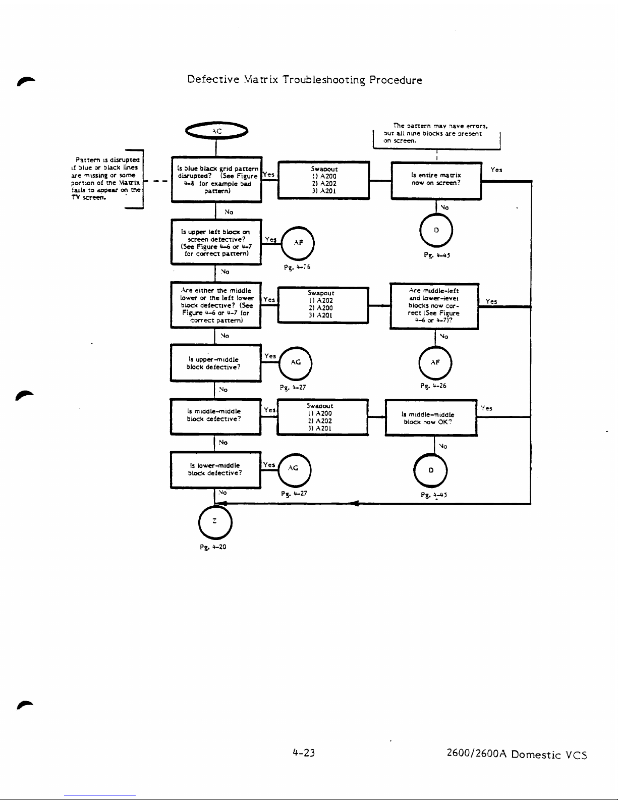
Partem
LS
disrupted
if
blue or
black
iines
are
.nusing
or
some
gortlon of me
.UPLX
farh
to
appear
a\
me
N
screen.
Defective
Man
ix
troubleshoot in^
Procedure
Re
sanern
may
?ave crrors,
3ur
all
nme blocks
are
sresent
I
I
9
I
(5
blue
bbck
gr~d
panern
jwao~t
+
Yes
disrupted?
(See
Fisure
!)
A200
L
entire
matrix
-
-
3-8
for example
Sad
2)
A202
now on
%reen?
panem)
3)
A201
I3
upper
left
bbcK
on
Pq.
G6
.ire
either
me
middle
lower
or
the
left
lower
3-
defutrve?
(See
Figure
4-6
or
4-7
for
correct
panern)
b
J
Swapou
t
Are
mtadle-left
1)
A202
ma
lower-kvet
blocks
now
cor-
Yes
2)
A200
3)
A201
rect
(See
Figure
a-6
or
b7)?
'Jo
block defecnve?
Pg.
L27
Pq.
'(-26
I
Is
lower-m~ddk
block
defective?
Pg.
b27
Pg.
b-4
A
-
u
Pg. '(-20
2600/2600A
Domestic
VCS
Page 67
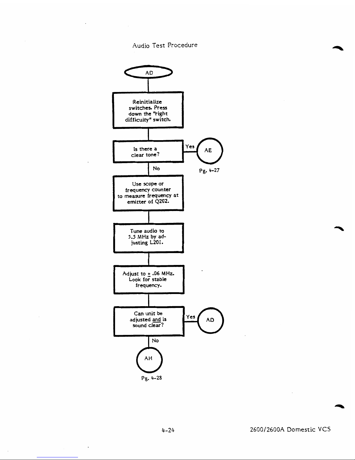
Audio
Test
Procedure
I
Reinitialize
switches. Press
down
the
'?right
difficulty
"
switch.
Is
there
a
clear
tone?
1
Pg.
4-27
Use
scope
or
frequency counter
to
measure
frequenq
at
emitter
of
QZOZ.
I
7)
Tune
audio
to
5.5
MHz
by
ad-
justing
L2O
1.
I
h
Ad
just
to
2
.06
MHz.
Look for
stable
f
r
tquency.
Can
unit
be
adjusted
is
sound
clear?
Pg.
4-28
2600/2600A
Domestic
VCS
Page 68
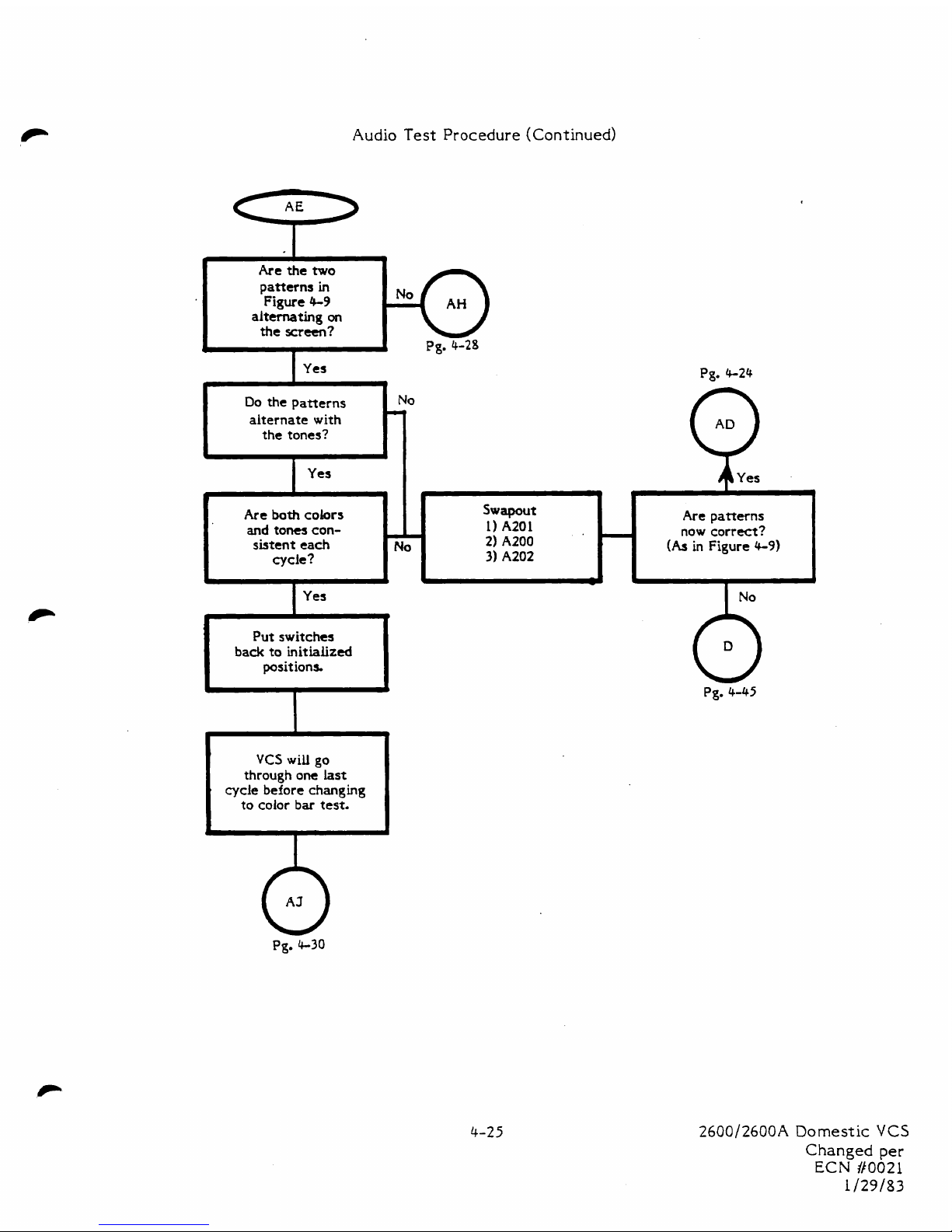
Audio Test Procedure (Continued)
Are
the
two
I
patterns
in
Figure
4-9
alternating
on
the
screen?
Pg.
4-28
I
Yes Pn.
4-24
Do
the
patterns
alternate with
the tones?
1
yes
I
Are
both
colors
and
tones con-
sisten
t
each
cycle?
I
Yes
1
-
Put
switches
back
to
initialized
positions.
b
VCS
will go
through om
last
cycle before changing
to
color
bar
test.
Pg.
4-30
A
J
2600/2600A Domestic
VCS
Changed
per
ECN
#0021
1/29/83
b
I
Are
patterns
now
correct?
(As
in
Figure
4-9)
No
Swapout
I)
A201
2)
A200
3)
A202
I
Page 69
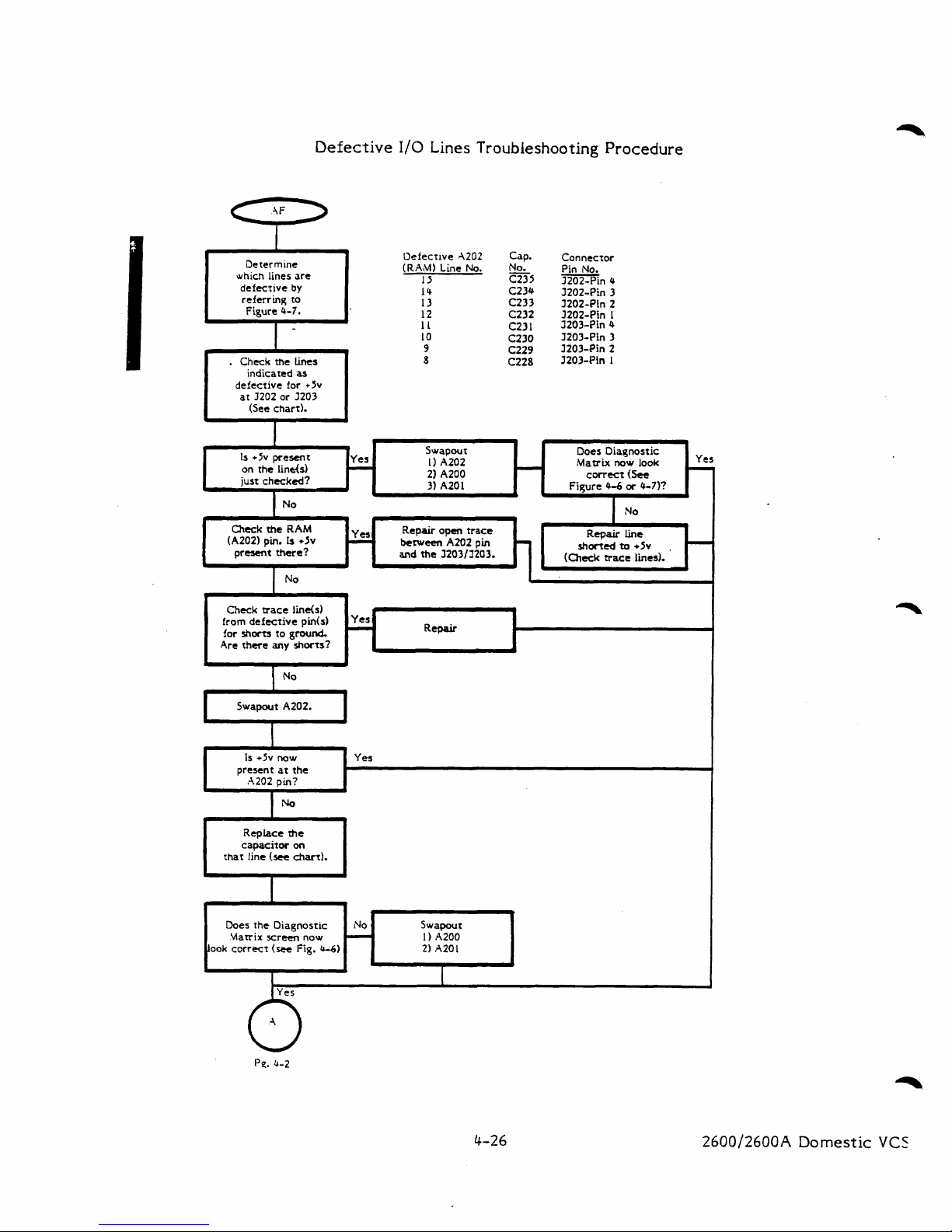
Defective
1/0
Lines
Troubleshooting Procedure
De
(ermine
which lines are
defective
by
referring to
.
Check
the
lines
indicated
as
defective for
+Sv
at
3202 or 3203
(See chart).
Uefect~ve
202
Cap.
Connector
(RAIM)L~~~No.
No.
PinNo.
15
C235 3202-Pin
u
14
C234 3202-Pin
3
I3
C233
3202-Pin 2
I*H-h
berwecn
AM2
pin
(A2021
pin.
Is
+5v
prtxnt
there?
and
the
3203D203.
I
b
1-k
(~hcd<
trace
lined.
I
Is +5v
now
Yes
present
at the
I
.
I
Swapout
I)
A202
2)
A200
3)
A201
-
J
Is
+5v
present
on
the
linds)
just checked?
I
Check
trace linds)
from defective pin(s)
for
rhora
to
ground.
Are there
any
shorn?
I
A202
pin?
1
Replace
the
capacitor
on
that line
(see
chard.
I
Does Diagnostic
Matrix
now
look
cwrtct
(See
Figure
4-6
or
4-7)?
Yes
-
Does the Diagnostic Swapout
Matrix
screen
now 1)
A200
ook correct
(see
Fig.
b-6)
2)
A201
A
L
Yes
-
l
Yes
2600/2600A
Domestic
VC5
Repair
I
Page 70
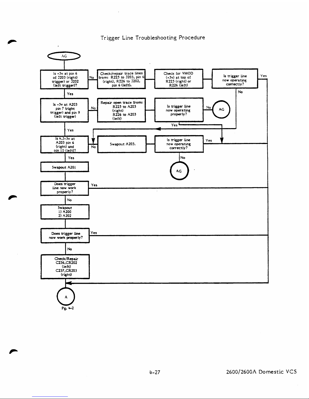
Trigger
Line
Troubleshooting Procedure
.I
Yes
I
I
C
1s
+Sv
at
A203
Repair
open
trace from:
No
R225
to
A203
Is
trigger Line
pin
7
(right
(right)
-
now
operating
trigger)
and
pin
9
-
R226
to
A203
properly?
(left trigger)
(left)
*
A
i
I
)
Yes
A
I
1
1
-
I
Yes
-
A
A
1
L
trigger
Line
now
operatins
correctly?
I
Check/Rtpair
C236,CRZOZ
(left)
C237,CR203
(right)
-
Check/repair
trace lines
from:
R225
to
3203,
pin
6
(right),
R226
to
3202,
pin
6
(left).
b
ls
+5v
at pin
6
of
3203
(right)
trigger) or
1202
(left trigger)?
t
b
4.5-5v
at
L
9
A203
pin
6
Swapout
A203.
-
(right)
and
No
I
Does
trigger
line
now
WQd
pmperly?
2600/2600A
Domestic
VCS
No
-
J
Is
trigger
line
nor operating
cofrectly
?
Yes
'
L
3
Check
for
VMOD
(+Sv)
at top of
R225
(right) or
R226
(left)
in
10
(left)?
-
I
Yes
L
Swapout
A201
I
I
Docs
trigger Yes
line
now
work
I
swapout
I)
A200
2)
A202
4
I
I
Page 71
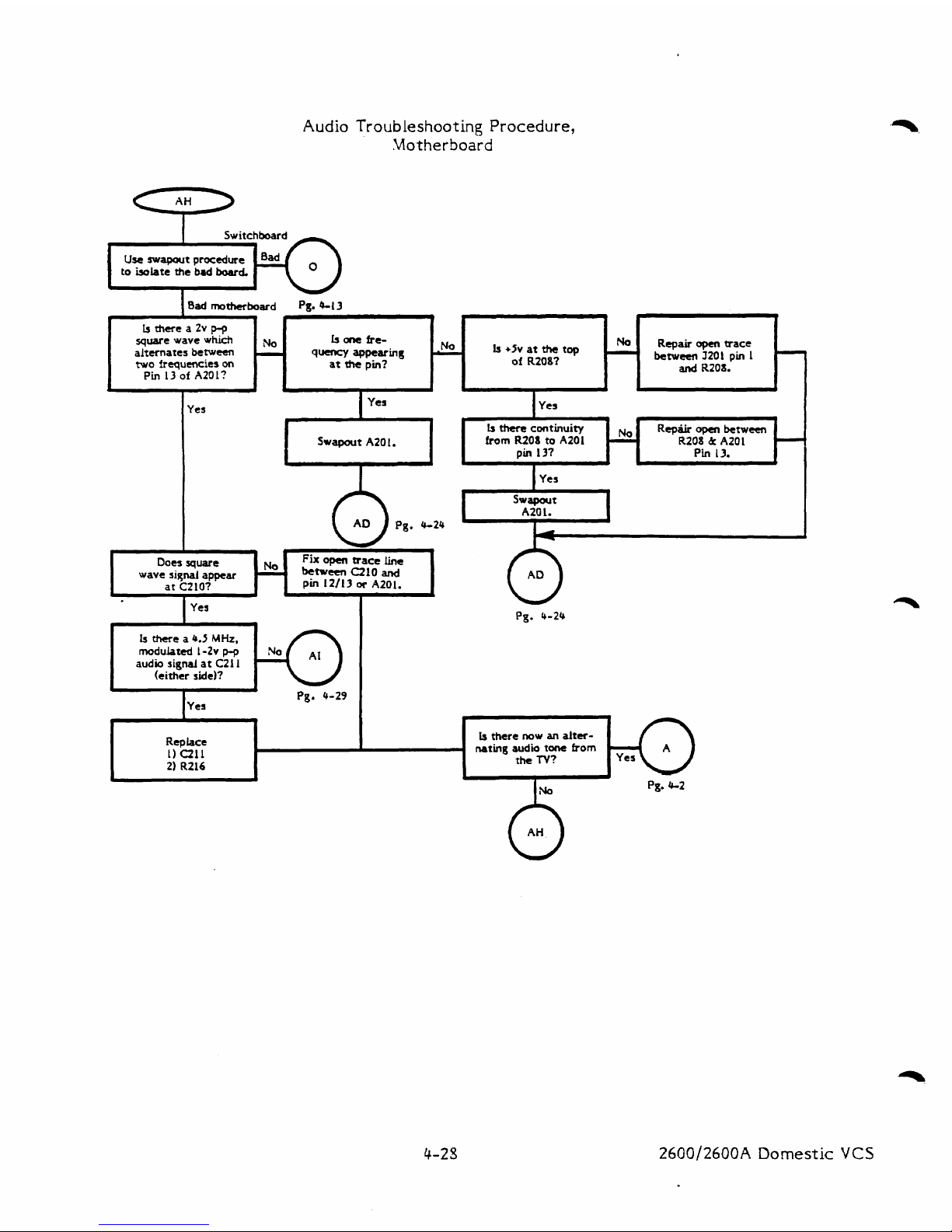
Audio
Troubleshooting
Procedure,
.Motherboard
Switchboard
to
isolate
the
bad
board.
I
BA
mmcrbovd
pg.
e
1
3
b
J
J
Isrhuea2vp-p
i
square wave whrd
b one
fre-
,.No
Is
+5v
at
the
top
NO
Repair
open
trace
alternates
betweal
-
quencY
aPWarh5
of
R2081
between
320
1
pin
1
two
frequencies
on
at
the
pin?
and
R201.
Pin
13
of
A201?
I
Yes
2600/2600A
Domestic
VCS
b
there
continuity
No
Rep%r
open
between
Swapout
A20
I.
from
R208 to
A201
-
R208 & A201
pin
131
Pin
13.
I
9
Replace
-
L
Is
there
now
an
alter-
_r
_I
L
I
I
Yes
Swapart
A20
I.
Pg.
4-24
.
L
Don
square
Fix
open
trace
line
wave siqnal
appear
betareen
C210
and
AD
at
C210?
pin
12/13
or
A201.
b
Pg.
4-24
k
there
a
4.5
MHz,
mduhtd 1 -2v
p-p
No
audio
signal
at
C2
1
1
(either
side)?
h
Pg.
4-29
Y
er
1)
all
21
RZ16
nating
audio
tone
from
the
N?
Pg.
4-2
Page 72
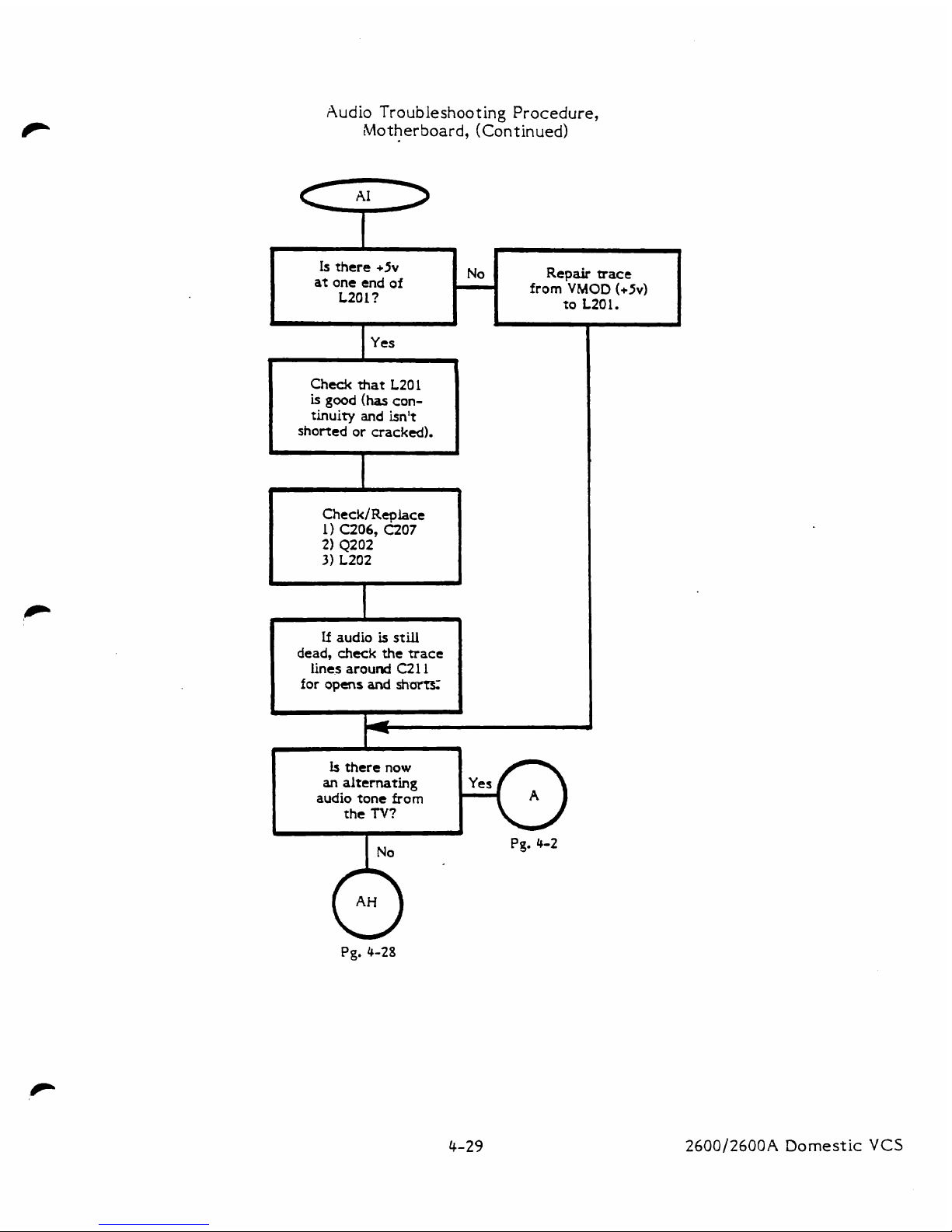
Audio
Troubleshooting Procedure,
Motherboard, (Continued)
I
Is
there
+5v
W
Repair
trace
at
one
end
of
from
VMOD
(+5v)
L20
1 ?
to 1201.
I
Check
that
L201
is
good
(has
con-
tinuity
and
isn't
shoned or
cracked).
1
I
If
audio
is
still
dead,
check
the
trace
lines
around
C2
1
1
for
opens
and
strons:
J
Is
there
now
an
alternating
Yes
audio
tone
from
the
TV?
Pg.
4-2
Pg.
4-28
2600/2600A
Domestic
VCS
Page 73

Cartridge Test Procedure
DTC
works,
but
VCS
unit
P
I
Plug
in
customer Not
Available
cartridge,
if
available.
w
I
6
Pg.
4-31
Available
Connect,
initialize,
and
turn
VCS
on
with
customer's game
cartridge.
Replace
with
good
cartridge.
Do&
correct
video
pattern
for
that
game
appear?
Pg.
4-45
No
A
Pg.
4-31
2600/2600A
Domestic
VCS
i
Yes
I
Play
game.
Does
it
',
Yes
play
OK?
a
L
No
Pg.
4-31
Yes
Check
customer
A
Swapout
I)
A201
Yes
Does
game
now
operate
I
properly
with
game
cartridge?
cartridge
on
known
good
game.
Is
it
OK?
rn
I
b
v
2)
A200
3)
A202
I
Page 74

Burn-In Procedure
Place
customer cartridge
in
game,
if
available.
Otherwise,
use
other
game cartridge.
J
Run game for
2
hours, minimum.
Do
not
turn
off
during this period.
Check game's
operation.
I
Is
game
working
properly?
I
Pg.
4-2
2600/2600A
Domestic
VCS
Page 75

Defective Switch Troubleshooting Procedure
Put
inoper-
ative switch
in
up
(open)
position.
I
Is
trace
3201
pin
for
that switch
line
shorted
(see
connection
chart)?
to
groud?
Yes
Repair
P
b
dv
now
present on
J2Ol
pin
for
that switch
(see
chart)?
Does
panun
on
Screen
change when
switch
b
flipped?
I
Is
on
side
of
switch
tied
,to
ground
as
Shown
in
schematic?
CONNECTION CHART
Switch
11
0 1 Pin
No.
lad<
h
White
4
Left
Difficulty
S
Right Difficulty
7
select
9
Reset
8
2600/2600A
Domestic
VCS
2'
Replace
switch
i
Page 76

Snowy Screen
Troubleshooting
Procedure
a
Is
there
dv
9
No
on
J201
pin 12?
Yes
I
I
Swapout A201.
I
w
Is
there
A
.
Yes
modulation?
m
4
1
h
Is
there
+5v
Is
there
NO
an
open
Line
on
pin
20 of
I
AZOI?
between
pin
20
and
+5v?
1
J
I
I
L
there continuity No
across
5201 pin 12?
Replace J20
1
r
Yes
L
I
I
Repair.
(
No
1
No
Yes
2600/2600A
Domestic
VCS
Yes
Replace
J
Is
J20l
pin
12
shorted to
ground?
(check
continuity)
'
&
Swapout A20
1.
I
Swapout
1)
A200
2)
A202
Is
there
modulation?
I
I
s
yes
J
Are C221 or
R223 shorted
to ground?
Repair
No
I
I
J
Check
for
solder bridges
or trace
shorts.
c
h
L
b
I
I
I
t
J
Page 77

Paddle
Lines
Test
Put
shorting
plugs
in.
Put
VCS
into
Diagnostic
Matrix
mode.
Swapout
0
A201
2)
A200
3)
A202
1
J
I
Is
there
con-
tinuity
between
the 1202 or 3203
pin
(see
chart)
and
the A20 I?
2
Checx
3202/3203
for
RC
waveform
(see
Fig.
4-10).
Is
waveform present on
each
of
the pins shorn
I
Yes
No
-
in
char??
Check
nace
lines
and
resistors for opens
.
rn
a
Repair
r
or
shorted.
DO
paddle lines now
work
OK?
b
k
RC
waveform
appear
on
the
appropriate J202
or J203 lie?
(Set
Chart)
Yes
Line
now
work?
tiepav
open
trace between
A201
and
12021
Yes
-
Yes
Connection
Chart
pg.
4-2
b
3293.
Pin
Pin
Pi
Cap
Plaver A201 3202
203
--
1
40
5
-
CZ15
2 39
9
-
C216
3
38
-
5
C217
4 37
-
9
C218
I
b
#
2600/2600A
Domestic
VCS
'~c.~:~~~2~~~t
shown
in the
chart?
&
Page 78

NOTE:
The following figures are referenced in
the
2600/2600A
Diagnosric Flowcharts,
Sections
4
and
6,
and are included here
for
your convenience. They can also
Se
found
in
Section
3,
where the
tests
are described in more detail.
initially
to
the
left
Figure
4-1. Switch Initialization Positions
2600/2600A
Domestic
VCS
Page 79

Figure
4-2.
Color
Bars
Screen
NDTE:
Set all switches to initialized position. A screen of horizontal color bars is
displayed (see Figure
4-2).
The screen should be steady and unchanging.
A
gray or
blue horizontal reference line runs across the screen about three bars from its bottom.
This
reference line is thinner than the bars around it. R211
(R213
on the 2600A board)
should be adjusted so the bars immediately above and below the reference line are
within one shade of each other. Proper operation of the unit is indicated
by
being able
to make this adjustment and by consistent color within the entire span of each bar on
the screen.
Minor glitches on the edges of the color
bars
are acceptable. Leave this
test
on for at least ten seconds in order to catch any intermittent problems, such
as a
bar
momentarily changing colors or blanking out.
2600/2600A Domestic
VCZ
Page 80

ANY
DIAGONAL
LINES
ON
THE
SCREEN
INDICATE
A
FAILURE
IN
THE
RAlU
CHIP
(A2'02).
Figure
4-3.
Defective
RAM
Patterns
2600/2600A
Domestic
VCS
Page 81
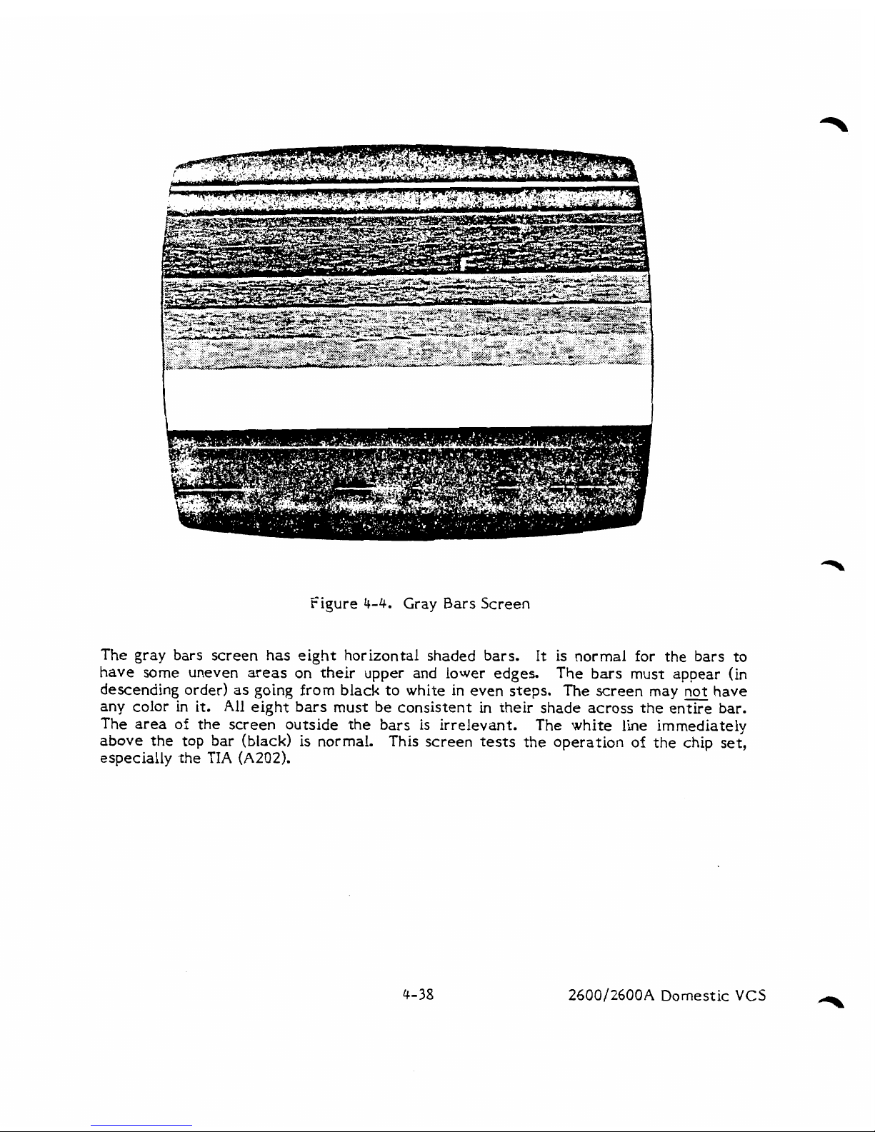
Figure
4-4.
Gray
Bars
Screen
The gray bars screen has eight horizontal shaded bars.
It
is normal for the bars to
have
some uneven areas on their upper and
lower
edges.
The
bars must appear (in
descending order) as going from black to white in even steps.
The
screen may
not
have
any color
in
it. All eight bars must be consistent
in
their shade across the entire bar.
-.
-
-
lhe
area
of
the screen outside the bars
is
irrelevant.
The white line immediately
above the top bar (black) is normal. This screen
tests
the operation
of
the chip set,
especially the TIA
(A202).
2500/2600A
Domestic
VCS
-
Page 82

Figure
4-5.
Defective Gray Bars Screen
This screen shows
an
example of a defective gray bars
test
screen.
The
appearance
of
a
black
rectangle
in
the middle of a light gray bar means that the data for that part
of
the screen has failed to
be
translated properly to the TV.
Any disruption of the
standard gray
bars
pattern (See Figure
4-4)
or any color
in
the gray bars screen
indicates a failure.
2600/2600A
Domestic VCS
Page 83
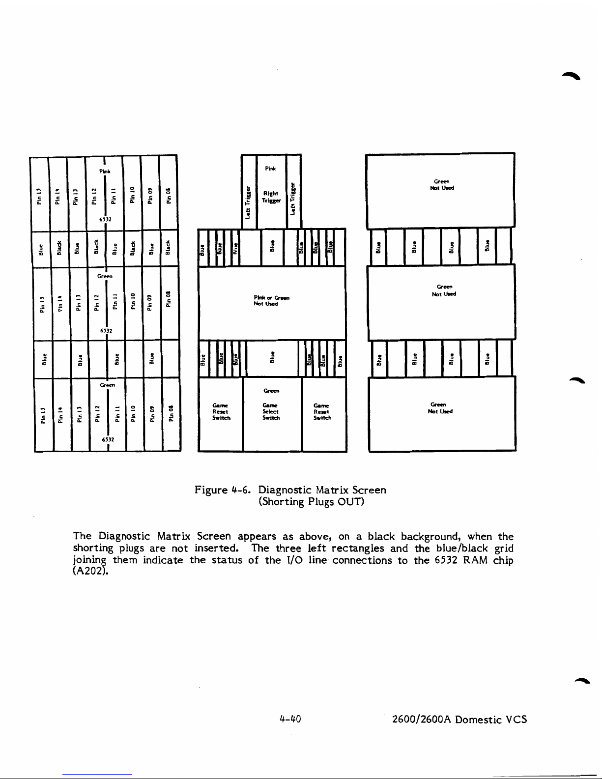
Gem
Not
Urd
Figure
4-6.
Diagnostic Matrix Screen
(Shorting Plugs OUT)
The Diagnostic Matrix Screen appears as above, on a black background, when the
shorting plugs are not inserted. The three left rectangles and the
blue/black grid
joinin them indicate the status
of
the
110
line connections
to
the
6532
RAM
chip
(A2028.
2600/2600A
Domestic
VCS
Page 84
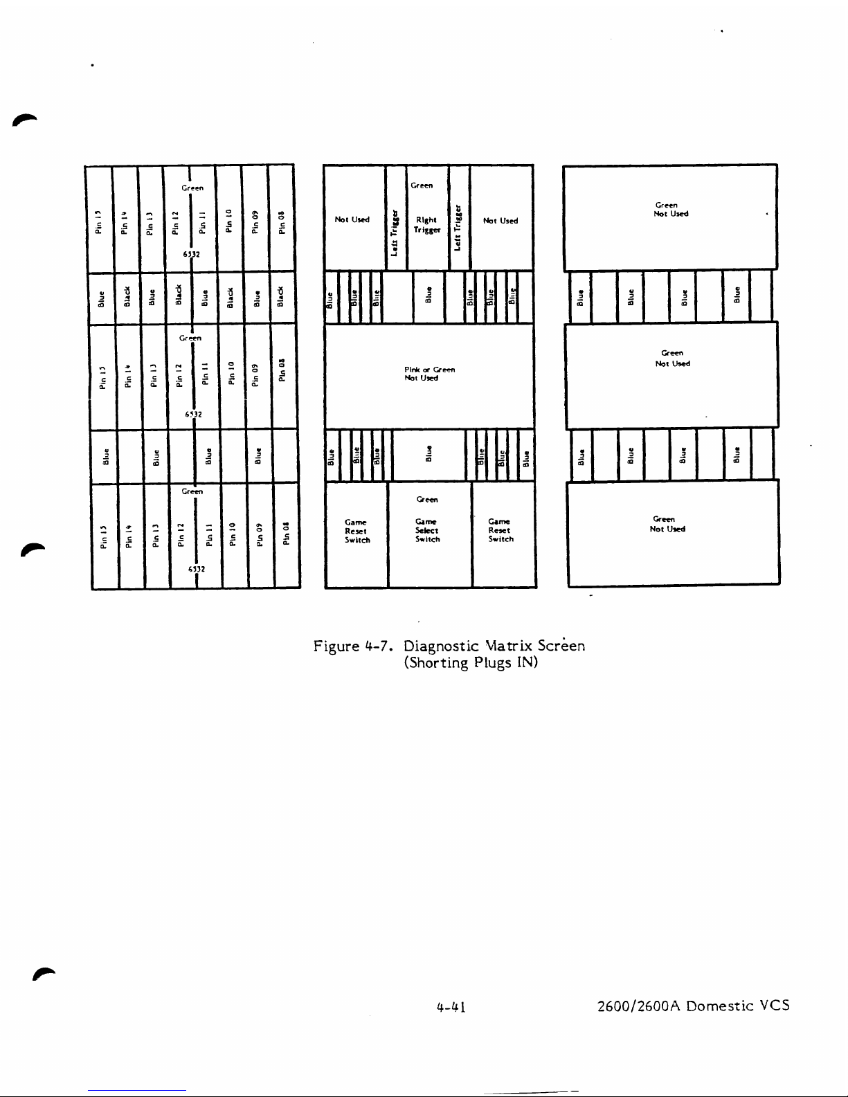
Page 85
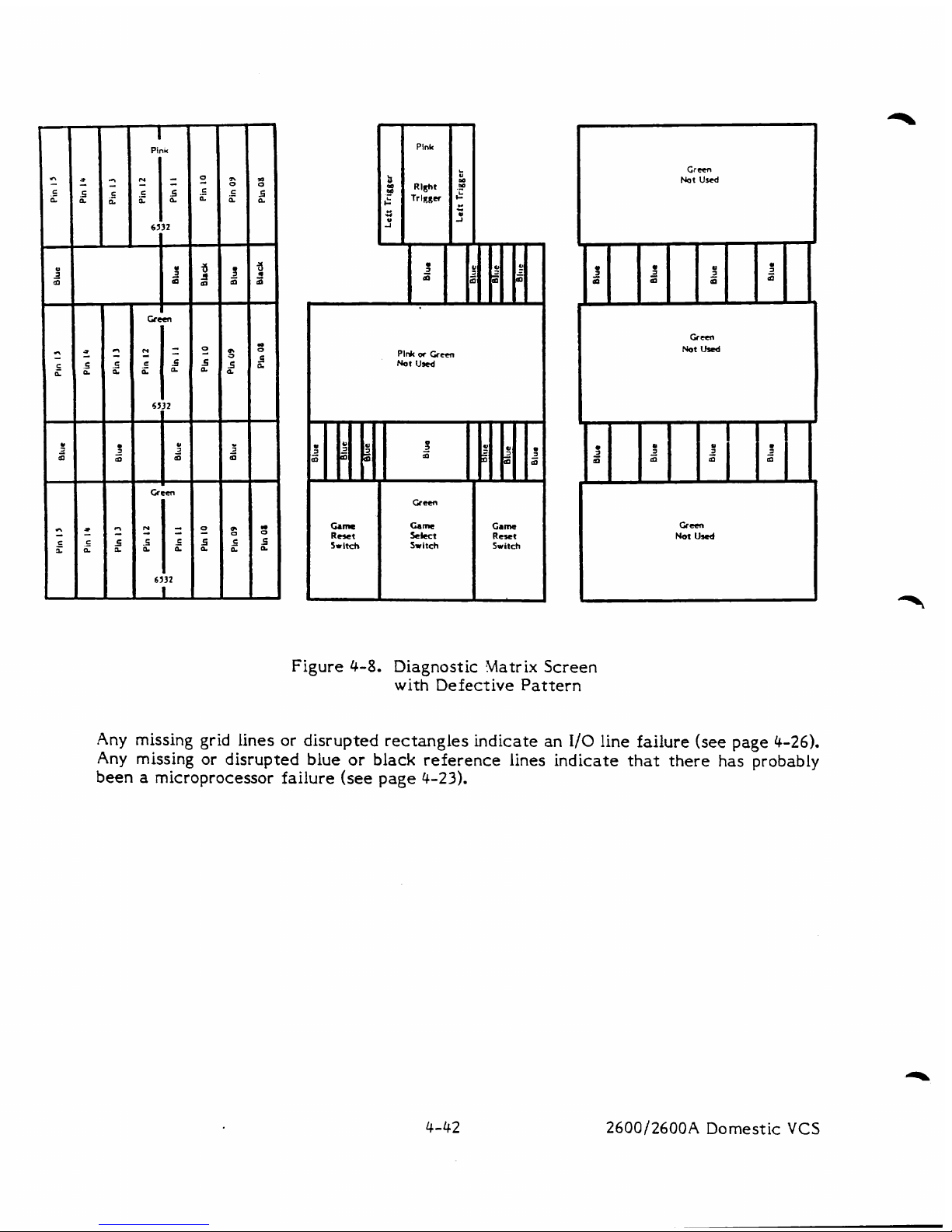
Pink
a
Getn
Not
Ud
C
r
een
Not
Used
Cunc
Ret
Switch
Gem
Not
UA
Figure
4-8.
Diagnostic
Va
tr ix Screen
with Defective Pattern
Came
kka
Switch
Any missing grid lines or disrupted rectangles indicate
an
I/O
line failure
(see
page
4-26).
Any missing
or
disrupted
blue
or black reference lines indicate that there has probably
been
a
microprocessor failure (see page
4-23).
Game
Rex
t
Switch
2600/2600A
Domestic
VCS
Page 86
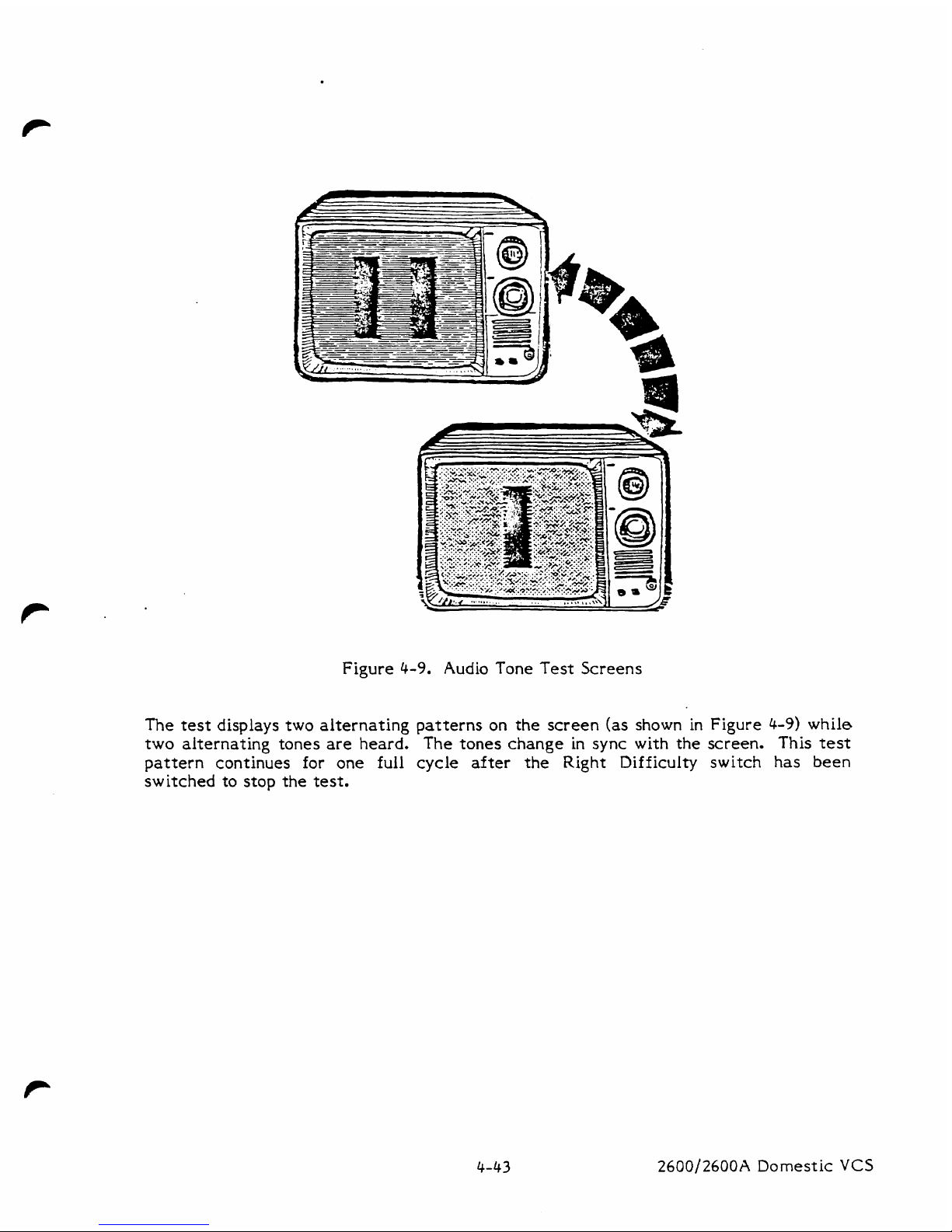
Figure
4-9.
Audio Tone Test Screens
The
test
displays two alternating patterns on the screen (as shown in Figure
4-9)
while
two alternating tones are heard.
The tones
change
in sync with the
screen.
This
test
pattern continues for one full cycle after the Right Difficulty switch has
been
switched to stop the test.
2600/2600A
Domestic
VCS
Page 87

2ms/div.
Iv/div
.
Pin
37
and
Pin
39
Figure
4-10.
RC
Waveforms
Zms/div.
Iv/div.
Pin
38
and
Pin
40
2600/2600A
Domestic
VCS
Page 88

The Signal Tracing Cartridge
(STC)
is used to locate easily open or shorted traces in
the address and data lines of the 2600/2600A. The STC causes the 6507
microprocessor
(AZOO) to cycle through the entire memory space while executing "no
operation" instructions.
This is valuable because it puts a known signal on each
address and data line. Then the signal can
be
traced through to the JZOO connector,
the TIA and RAM-I/O chips.
Since the STC procedure is not easily reduced to a flowchart, it is presented
as
a
series of written instructions and illustrations on the following pages.
CAUTION:
The
STC
procedure requires three
known-good
chips
and a working
clock
circuit.
The
STC
should
only
be
used
after
all
other procedures
have
been
tried.
GETTING STARTED
Insert the STC into the 2600/2600A.
Turn on the unit. The television screen should be
gray or black. If it is "snowy" it indicates that you should return to the start of the
Diasnostic Flowchart. Set the scope sweep to
.5
microsec/division and set the vertical
to
1
volt/division.
ADDRESS LINES
AB@-
AB12
Check the address lines at-the microprocessor (H200). Check address lines, startins
wirh pin
5.
A
signal with a waveform similar to those shown in Figure 4-1 1 should be
seen on the address lines, with each succeeding address line's waveform having
a
frequency half that of the line before
it.
For example, A1 should be half the
frequency of
.A@.
If one or more of the address lines shows no signal, it is likely that
the line is either open or shorted to ground or +5v.
Check all traces and pins for
shorts.
If you have a defective address line and it is not open or shorted,
swapout the A200,
A202 and
A201,
in that order.
If all address lines have signals, trace those signals to the
JZOO
and the other chips.
Table 4-1 illustrates which address lines connect to which pins on 3200,
6532,
and the
A. The signal present on each address line of the microprocessor should also be
present on each pin of 3200,
6532,
and the
TIA
connected to that line.
If
the same
signal is not found, the trace line and/or solder joints between the microprocessor and
the dead pink) is (are) broken. Check the trace lines carefully to locate the break.
DATA LINES
DBO-7
Set the v~rtical on your scope to Zv/division. The data lines are tested very much like
the address lines. The only difference is that
the
waveform seen on the data lines is
different.
The signals you should see are illustrated in Figure 4-12.
If
any data lines
are completely inactive (simply remaining a constant voltage), it probably means that
the line is either open or shorted to ground
or
+5v.
Check the traces and pins for
P
shorts. If none are found, one of the three chips or the STC itself probably has an
internal short. Try swapping out the 6532, TIA, and the microprocessor. Also
carefully check J2OO for shorts between pins.
4-45 2600/2600A Domestic
VCS
Page 89
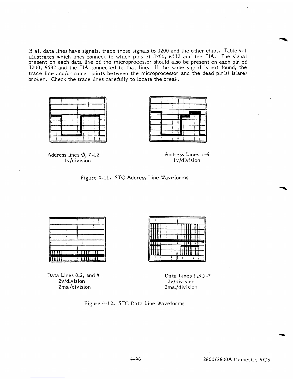
If
all data lines have signals, trace those signals to JZOG and the other chips. Table 4-1
illustrates which lines connect to which pins of 3200,
6532
and
the
TIA.
The signal
present on each
data
line of the microprocessor should also be present on
each
pin
of
3200,
6532
and the TIA connected to that line.
If the same signal is not found, the
trace line and/or solder joints between the microprocessor and the dead pin(s) idare)
broken. Check the trace lines carefully to locate the break.
Address lines
@,
7-12
1
vldivision
Address
Lines
1-6
1
v/division
Figure
4-1
1.
STC
Address Line Waveforms
I
I
'
I
t
1
.
,
I!,
Data Lines 0,2, and
4
2v/division
2 ms./division
Data Lines 1,3,5-7
2v/division
2ms./division
Figure 4-12.
STC
Data
Line
Waveforms
2600/2600A Domestic
VCS
Page 90

TABLE
4-1
Connected
Pins
on Motherboard
ADDRESS
LINES
A20
2
A202
5200
(TIA)
(RAM)
Connector
ABO
.
5
32
7
8
DATA
LINES:
DBO
25
14
33
9
--
Indicates
no
connection on
that
line
2600/2600A
Domestic
VC5
Page 91
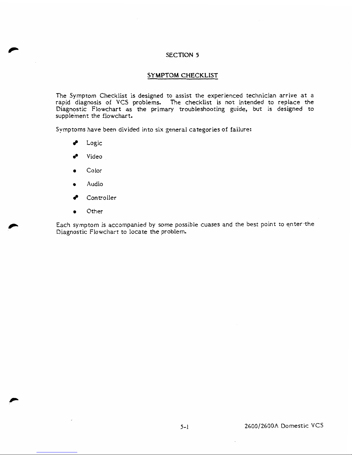
SECTION
5
SYMPTOM
CHECKLIST
The Symptom Checklist
is
designed to assist the experienced technician arrive
at
a
rapid diagnosis
of
VCS
problems. The checklist is not intended to replace
the
Diagnostic Flowchart
as
the
primary troubleshooting
guide,
but
is
designed to
supplement the flowchart.
Symptoms
have
been divided into six general categories of failure:
Logic
Video
a
Color
a
Audio
Controller
a
Other
Each symptom is accompanied
by
some
possible cuases and the best point to enter -the
Diagnostic Flowchart to locate the problem.
2600/2600A
Domestic
VCS
Page 92

2600
FAILURES
LOGIC
FAILURES
DIAGNOSTIC
POSSIBLE
CAUSE
POSSIBLE
CAUSE
FLOWCHART
SYMPTOM
(mother
board)
(switchboard)
ENTRY
POINT
Solid colored A200, A202, TIA A101,RFModule
J,pg.4-9
screen X200, 4200, 4201,
open or shorted
Address or Data line
Vertical lines ,4200,
A201,
A202,
5200, open
or
shorted Address or
Data
line
J,
pg.
4-9
VIDEO
FAILURES
DIAGNOSTIC
POSSIBLE
CAUSE
POSSIBLE
CAUSE
FLOWCHART
SYMPTOM
(mother
board)
(switchboard)
ENTRY
POINT
Snowy
screen no power,
A203
A101, L101,
RF
L,
pg.
4-1
1
5201, J204
Module,
J
10 1
Weak
picture
N/
A
Wronrg
Gray
Bars A201, A203,
R2
18-R220
LlOl,RFModule, X,pg.4-18
RF
Cable
P,
pg.
4-14
-
2600/2600A Domestic
VCS
Page 93

2600
FAILURES
(Continued)
CDLOR
FAILURES
SYMPTOM
No color
Only the
reference
bar
appears
Color won't
ad
just
Veak color
I
SYMPTOM
No audio
'Afeak
audio
DTC
audio
test
fails
DIAGNOSTIC
POSSIBLE
CAUSE
POSSIBLE
CAUSE
FLOWCHART
(motherboard) (switchboard)
ENTRY
POINT
L101,
RF
Module
AA,
pg.
4-21
RF
Cable
C208, R211
N/
A
RA,
pg.
4-21
R211, C208, C209
N/A
AA,
pg. 4-21
C212,
C213, R215
RF
Module, LlOl
AA,
pg.
4-21
RF Cable
AUDIO
FAILURES
DLAGNOSTIC
POSSIBLE
CAUSE
POSSIBLE CAUSE
FLOWCHART
(motherboard)
(switchboard)
ENTRY
POINT
C206,
C207,
L201
RF
module AH,
pg.
4-25
adjustment, 4202 adjustment
,4201, C206,
C207,
XF
module
AH,
pg.
4-28
L201 adjustment, adjustment
C20
1
.42C11,
A200,
A202
N/
A
AD,
pg.
4-24
2600/2600A
Domestic
VCS
Page 94

2600
FAXLURFc
(Continued)
CONTROLLER
FAILURES
DIAGNOSTIC
POSSIBLE
CAUSE
POSSIBLE
'CAUSE FLOWCHART
SYMPTOM
(motherboard) (switchboard)
ENTRY
POINT
Fire button A203, 5202, 5203,
N/A
does
not work
defective
Con
troller
AG,
pg.
4-27
Joystick
does
A202, 5202, 3203,
not work
defective Joystick
N/A
AF,
pg.
4-26
Dr
ivin?
A202, J202, 5203
N/
A
AF,
pg.
4-26
Cunlroiier
s
defective Con troller
Paddle A20 1, C215-C218,
N/
A
pg.
4-34
Controllers 5202
-
3203,
defective controller
OTHER FAILURES
DIAGNOSTIC
POSSIBLE
CAUSE
POSSIBLE
CAUSE
FLOWCHART
SYMPTOM
(motherboard) (switchboard)
ENTRY
POINT
Switches A202, C222-C227 S102-S106,
JIOl
AL,
pg.
4-32
not working
-
2600/2600A
Domestic
VCS
Page 95

2600A
FAILURES
LOGIC
F.ULURES
(2600A)
DIAGNOSTIC
FLOWCHART
POSSIBLE
CAUSE
ENTRY
POINT
SYMPTOM
Solid colored
screen
A200, A202, A20
1,
I,
pg.
6-10
X200, 4200,
RF
Module
Vertical lines
A200,
A201, A202,
I,
pg.
6-10
3200, open or
shorted
Address
or
Data
line
VIDEO
FAILURES (2600A)
DIAGNOSTIC
FLOWCHART
ENTRY
POINT
POSSIBLE
CAUSE
SYMPTOM
Snowy screen
A203,
5201,
RF
Vodule, L205
K,
pg. 6-12
K,
pg. 6-12
M,
pg.
6-14
RF
Module,
RF
Cable
Weak picture
Vrong Gray Bars
Revisions 1
-1
3
N,
pg.
6-15
Wrong Gray
Bars
Revision
14
C,
pg.
6-4
Cl,
pg.
6-5
Warped picture
Revisions 1-13
Warped picture
Revision 14
..
2600j2600A
Domestic
VCS
Page 96
2600A
FAILURES
(Continued)
COLOR
FAILURES
(2600A)
DIAGNOSTIC
FLOW
CHART
ENTRY
POINT
SYMPTOM
No
color
POSSIBLE
CAUSES
X200,
A201,
C210,
C211
RF
Cable
P,
pg.
6-16
Only
the
reference bar appears
Color won't
ad
just
P,
pg.
6-16
Weak color
RF
Module, C210,
C211,
RtlO,
RF
Cable
AUDIO
FAILURES
(2600A)
DIAGNOSTIC
FLOW
CHART
ENTRY
POINT
SYMPTOM
POSSIBLE
CAUSES
No
audio
4
C206,
.
C207,
420
1,
R F Module ad just
ment
Weak
audio
A201,
C208,
R207,
C2O6,
C207,
RF
Module adjustment
X,
pg.
6-24
Diagnostic
test
cartridge
audio
test
fails
X,
pg. 6-24
2600/2600A Domestic
VCS
Page 97
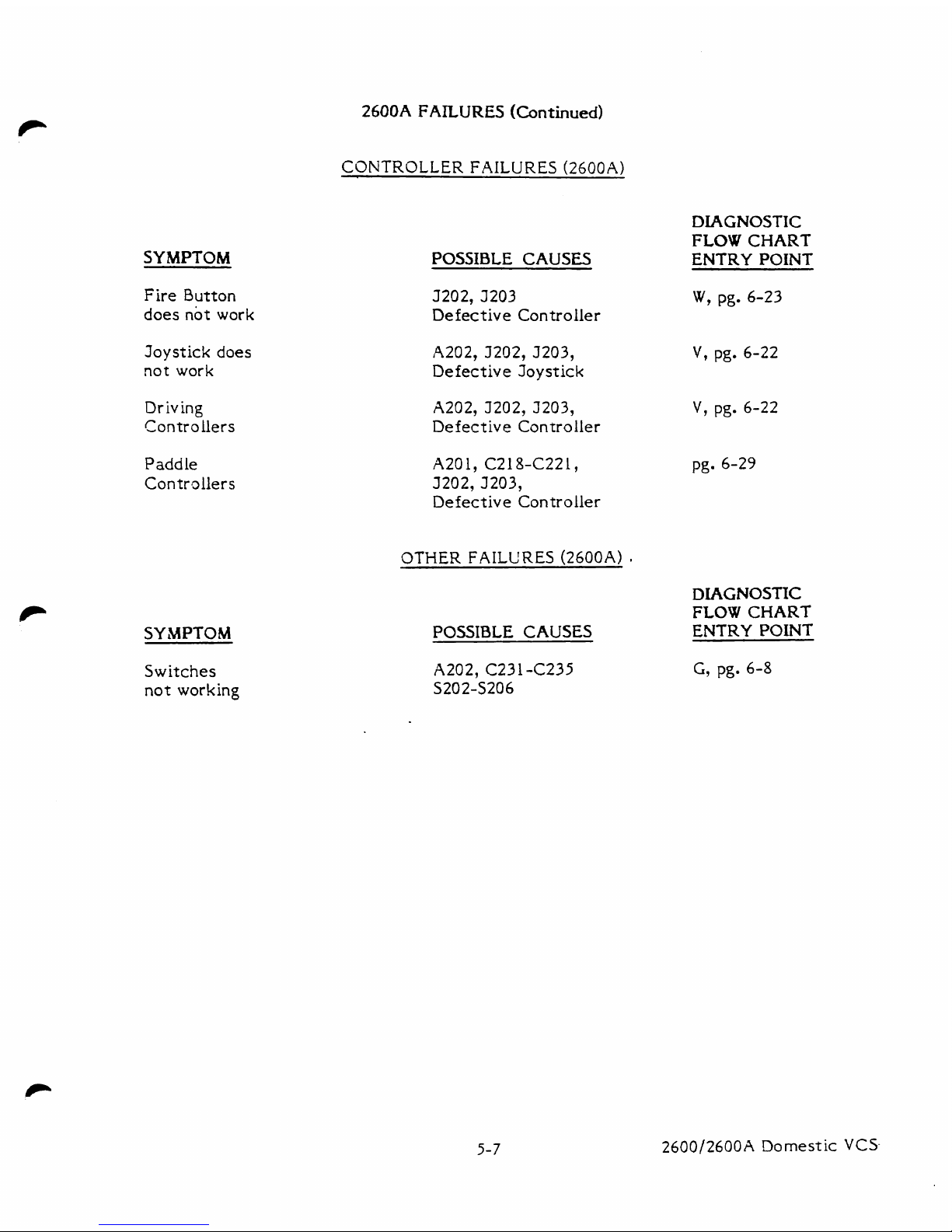
SYMPTOM
Fire Button
does
not
work
Joystick
does
not work
Driving
Controllers
Paddle
Controllers
SYMPTOM
Switches
not working
2600A
FAILURES
(Continued)
CONTROLLER
FAILURES
(2600A)
POSSIBLE
CAUSES
5202, 5203
Defective Controller
A202, 5202, 5203,
Defective Joystick
A202, 5202, 3203,
Defective Controller
3202, 3203,
Defective Controller
OTHER
FAILURES
(2600A)
POSSIBLE
CAUSES
DIAGNOSTIC
FLOW
CHART
ENTRY
POINT
W,
pg. 6-23
V,
pg.
6-22
V,
pg.
6-22
pg. 6-29
DIAGNOSTIC
FLOW
CHART
ENTRY
POINT
G,
pg.
6-8
2600/2600A
Domestic
VCS-
Page 98
SECTION
6
2600A
DIAGNOSTIC
FLOWCHART
The Diagnostic Flowchart is intended to be easy to use and the primary aid when
troubleshooting the 2600A.
Follow the prompts in the order presented.
The figures
referenced in the flowcharts are located at the end of Section
4,
beginning on page
4-37.
'When a question is asked, follow the line from that box which best applies to the unit's
situation.
When
a
line terminates with a letter inside a circle, note that a page number
(i.e.,
pg.
6-3)
is near it. Turn to that page, locate the letter in another circle, and
continue the diagnosis. The flowchart leaves nothing to chance, it
tells
you when to
perform
a
specific test, and when to replace components, and even when and how long to
"burn-in" the unit. "Burn-in" the unit for at least two hours after completing repairs.
When a problem is extremely difficult to diagnose, the flowchart sends you to the Signal
Tracing Cartridge (STC) routine,
"D",
page
4-47.
Due to the repetitive nature of the
STC
routine, no flowchart is used.
Read
and follow the instructions
as
directed. Should
the STC procedure fail to isolate the problem, after carefully inspecting the
motherboard assembly for shorted and/or
ooen trace lines and solder bridges, swap all
three chips (6507, 6532, and
TIA). Should
the
problem still persist, call
ATARI,
Techline
Specialist: Inside California
at
(800)
672-1
466
and Outside California at
(800)
538-1
535.
Be certain to always burn-in the unit for two hours after completing repairs. This helps
to ensure that intermittent problems are found and also greatly increases your
customer's satisfaction with your repair work.
,
SWAP
OUT
PROCEDURES
Many places in the diagnostic flowchart; a box tells you to "swapout"
a
chip or a number
of chips in
a
particular order. The "swapout" instruction means that you should replace
the indicated components one
at
a
time with a known good component of the same type.
The
VCS
should then be tested with the new, known-good com~onent in place to see
whether the "swapout" solved the problem being checked. If the swapout did not fix the
~roblern, the known-good component should be left in, and the- next component inserted.
Once the problem is solved, you then place the suspected bad chips one
by
one into the
system to determine whether
or
not those you pulled out are truly defective. In this
way, you avoid needlessly replacing good components.
CAUTION:
Extreme care should
be
taken
when
handling
the
intergrated circuit
chips
(A200,
A201,
A202,
AZ03).
They
are
all
very
sensitive to static electricity and
can
easily
be
damaged
by
careless handling.
Always
keep
the
chips
in
their plastic
carrier
tubes or on
conductive foam when not
handling
them.
Make
certain
you
are
well
grounded
when
handling
the
chips.
Atari
strongly recommends that you
wear
a
conductive grounding
band
(which
ties
from
your
arm
to
ground) when handling
the
chips.
The
chips
are
also
susceptible to damage
from
stress
when
being
removed from or
inserted
into
the
sockets.
Always
use
a
chip-puller when removing
the
chips.
Do
not
pty
chips out
with
a
screwdriver or
any
other
tool.
Failure
to
follow
the
above
guidelines results
in
unusually
high
chip
failure
rates
and
P
extra
expense.
2600/2600A
Domestic
VCS
Page 99

2600A
Diagnostic
Flowchart
Visually
in&
switches,
jacks
and
connectors
Makeccnainno
rhocted
I
oc
opn
traces
or
solder
bridg-
are
on
the
board(s1.
Tf
bancry
elimi-
nator.
Set
TV
to
n
In-
Diagnostic
Caruidge
(DTC),
in-
itialize
(Figure
b-1)
Does
any
dt-
Is
picture
Pam
appeu
onxsmn(xt
on
left
side
Pg.
6-5
Fig.
4-31.
of
sixem?
C
-
2600A
Revs
1-L3
C1
-
2600A
Revs
14
and
up
I
>
b
J
~unitnow&owthc
No
swapout
Does
unit
now
-
No
color
bars
pattun?
1)
A200
show
the
color
2)
A202
b
bars
pattern?
I
8
&
I.
2600/2600A
Domestic
VCS
Page 100
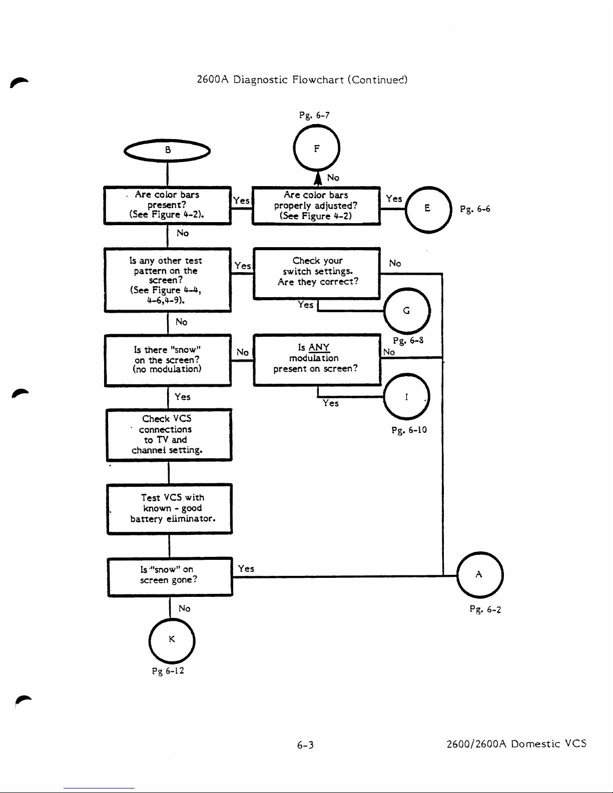
2600A
Diagnostic
Flowchart
(Continue?)
Pg.
6-7
-
Are
color
bars
Are color
bars
present?
.Yes
properly
adjusted?
Pg.
6-6
(See
Figure
4-21.
(See
Figure
11-21
4
h
No
Is
any
other
test
Check
your No
pattern on the
,
Yes
switch
seeings.
screen? Are they correct?
(See
Figure
4-4,
44,409).
1
Yes
Check
VCS
'
connections
to
N
and
cfiannel
setting.
I
Test
VCS
with
known
-
good
battery eliminator.
I
present on screen?
Pg.
6-10
2600/2600A
Domestic
VCS
I
IS
-"snow"
on
screen gone?
Yes
r
 Loading...