

Page 1

R
KN97
Pentium® II Motherboard
USER’S MANUAL
Page 2

USER'S NOTICE
No part of this manual, including the products and softwares described in it, may be reproduced, transmitted, transcribed, stored in a retrieval system, or translated into any language
in any form or by any means, except documentation kept by the purchaser for backup purposes, without the express written permission of ASUSTeK COMPUTER INC. (“ASUS”).
ASUS PROVIDES THIS MANUAL “AS IS” WITHOUT WARRANTY OF ANY KIND,
EITHER EXPRESS OR IMPLIED, INCLUDING BUT NOT LIMITED TO THE IMPLIED
W ARRANTIES OR CONDITIONS OF MERCHANTABILITY OR FITNESS FOR A PARTICULAR PURPOSE. IN NO EVENT SHALL ASUS, ITS DIRECTORS, OFFICERS,
EMPLOYEES OR AGENTS BE LIABLE FOR ANY INDIRECT, SPECIAL, INCIDENTAL, OR CONSEQUENTIAL DAMAGES (INCLUDING DAMAGES FOR LOSS OF
PROFITS, LOSS OF BUSINESS, LOSS OF USE OR DAT A, INTERRUPTION OF BUSINESS AND THE LIKE), EVEN IF ASUS HAS BEEN ADVISED OF THE POSSIBILITY
OF SUCH DAMAGES ARISING FROM ANY DEFECT OR ERROR IN THIS MANUAL
OR PRODUCT.
Products and corporate names appearing in this manual may or may not be registered trademarks or copyrights of their respective companies, and are used only for identification or
explanation and to the owners’ benefit, without intent to infringe.
• Intel, LANDesk, and Pentium are registered trademarks of Intel Corporation.
• IBM and OS/2 are registered trademarks of International Business Machines.
• Symbios is a registered trademark of Symbios Logic Corporation.
• Windows and MS-DOS are registered trademarks of Microsoft Corporation.
• Sound Blaster AWE32 and SB16 are trademarks of Creative Technology Ltd.
• Adobe and Acrobat are registered trademarks of Adobe Systems Incorporated.
The product name and revision number are both printed on the board itself. Manual revisions
are released for each board design represented by the digit before and after the period of the
manual revision number. Manual updates are represented by the third digit in the manual
revision number.
For previous or updated manuals, BIOS, drivers, or product release information, contact ASUS
at http://www.asus.com.tw or through any of the means indicated on the following page.
SPECIFICATIONS AND INFORMATION CONTAINED IN THIS MANUAL ARE FURNISHED FOR INFORMATIONAL USE ONLY, AND ARE SUBJECT TO CHANGE AT
ANY TIME WITHOUT NOTICE, AND SHOULD NOT BE CONSTRUED AS A COMMITMENT BY ASUS. ASUS ASSUMES NO RESPONSIBLITY OR LIABILITY FOR
ANY ERRORS OR INACCURACIES THAT MA Y APPEAR IN THIS MANUAL, INCLUDING THE PRODUCTS AND SOFTWARES DESCRIBED IN IT.
Copyright © 1997 ASUSTeK COMPUTER INC. All Rights Reserved.
Product Name: ASUS KN97
Manual Revision: 1.03
Release Date: July 1997
2
ASUS KN97 User’s Manual
Page 3

ASUS CONTACT INFORMATION
ASUSTeK COMPUTER INC.
Marketing Info
Address: 150 Li-Te Road, Peitou, Taipei, Taiwan 112, ROC
Telephone: +886-2-894-3447
Fax: +886-2-894-3449
Email: [email protected]
Technical Support
Fax: +886-2-895-9254
BBS: +886-2-896-4667
Email: [email protected]
WWW: www.asus.com.tw
Gopher: gopher.asus.com.tw
FTP: ftp.asus.com.tw/pub/ASUS
ASUS COMPUTER INTERNATIONAL
Marketing Info
Address: 721 Charcot Avenue, San Jose, CA 95131, USA
Telephone: +1-408-474-0567
Fax: +1-408-474-0568
Email: [email protected]
Technical Support
ASUS COMPUTER GmbH
Marketing Info
Address: Harkort Str. 25, 40880 Ratingen, BRD, Germany
Telephone: 49-2102-445011
Fax: 49-2102-442066
Email: [email protected]
Technical Support
ASUS KN97 User’s Manual 3
Page 4

CONTENTS
I. INTRODUCTION 7
How this Manual is Organized ........................................................... 7
Item Checklist ..................................................................................... 7
II. FEATURES 8
Features of the ASUS KN97 Motherboard ......................................... 8
The ASUS KN97 Motherboard ..................................................... 9
III. INSTALLATION 10
Layout of the ASUS KN97 Motherboard ......................................... 10
Installation Steps............................................................................... 12
1. Jumpers ......................................................................................... 12
Jumper Settings ..................................................................... 13
2. System Memory (SIMM)............................................................. 16
SIMM Memory Installation................................................... 17
3. Central Processing Unit (CPU).................................................... 18
AAVID Heatsink ................................................................... 22
Elan V ital Heatsink................................................................ 22
Pentium Pro SEC Card .......................................................... 23
4. Expansion Cards ........................................................................... 25
Expansion Card Installation Procedure ................................. 25
Assigning IRQs for Expansion Cards.................................... 25
Assigning DMA Channels for ISA Cards.............................. 26
ISA Cards and Hardware Monitor ......................................... 26
5. External Connectors..................................................................... 27
Power Connection Procedures .................................................... 33
IV. BIOS SOFTWARE 34
Support Software .............................................................................. 34
Flash Memory Writer Utility ............................................................ 34
Main Menu ............................................................................ 34
Advanced Features Menu ...................................................... 35
Updating your Motherboard’s BIOS ........................................... 36
6. BIOS Setup .................................................................................. 37
Load Defaults ........................................................................ 38
Standard CMOS Setup ................................................................ 38
Details of Standard CMOS Setup:......................................... 38
BIOS Features Setup ................................................................... 41
4
ASUS KN97 User’s Manual
Page 5

CONTENTS
Details of BIOS Features Setup............................................. 41
Chipset Features Setup ................................................................ 44
Details of Chipset Features Setup.......................................... 44
Power Management Setup........................................................... 47
Details of Power Management Setup .................................... 47
PNP and PCI Setup ..................................................................... 49
Details of PNP and PCI Setup ............................................... 49
Load BIOS Defaults .................................................................... 51
Load Setup Defaults .................................................................... 51
Smart Alarm (LM78) Setup ........................................................ 52
Details of Smart Alarm (LM78) Setup .................................. 52
Supervisor Password and User Password ................................... 53
IDE HDD Auto Detection ........................................................... 54
Save & Exit Setup ....................................................................... 55
Exit Without Saving .................................................................... 55
V. DESKTOP MANAGEMENT 56
Desktop Management Interface (DMI)............................................. 56
Introducing the ASUS DMI Configuration Utility ................ 56
System Requirements ............................................................ 56
Using the ASUS DMI Configuration Utility ......................... 57
VI. ASUS PCI SCSI Cards 59
Symbios SCSI BIOS and Drivers ..................................................... 59
ASUS PCI-SC200 & PCI-SC860 SCSI Cards ................................. 59
Setting Up the ASUS PCI-SC200 & PCI-SC860 ........................ 60
Setting the INT Assignment for the ASUS PCI-SC200 .............. 60
Terminator Requirements for SCSI Devices ............................... 60
Terminator Settings for the ASUS PCI-SC860 ........................... 61
Terminator Settings for the ASUS PCI-SC200 ........................... 61
SCSI ID Numbers for SCSI Devices .......................................... 62
SCSI ID Priority .......................................................................... 62
VII. ASUS I-A16C Audio Card 63
ASUS I-A16C Audio Features .................................................... 63
Unpacking and Handling Precautions ......................................... 63
Connectors ............................................................................. 64
CD-Audio Connector Pin Definitions ......................................... 64
AUDIO
Online help is provided with the Creative 16X audio drivers. A separate manual is
provided for the Creative 16C Series audio drivers.
ASUS KN97 User’s Manual 5
Page 6

FCC & DOC COMPLIANCE
Federal Communications Commission Statement
This device complies with FCC Rules Part 15. Operation is subject to the following
two conditions:
• This device may not cause harmful interference, and
• This device must accept any interference received, including interference that
may cause undesired operation.
This equipment has been tested and found to comply with the limits for a Class B
digital device, pursuant to Part 15 of the FCC Rules. These limits are designed to
provide reasonable protection against harmful interference in a residential installation. This equipment generates, uses and can radiate radio frequency energy and, if
not installed and used in accordance with manufacturer's instructions, may cause
harmful interference to radio communications. However, there is no guarantee that
interference will not occur in a particular installation. If this equipment does cause
harmful interference to radio or television reception, which can be determined by
turning the equipment off and on, the user is encouraged to try to correct the interference by one or more of the following measures:
• Re-orient or relocate the receiving antenna.
• Increase the separation between the equipment and receiver.
• Connect the equipment to an outlet on a circuit different from that to which
the receiver is connected.
• Consult the dealer or an experienced radio/TV technician for help.
WARNING! The use of shielded cables for connection of the monitor to the
graphics card is required to assure compliance with FCC regulations. Changes
or modifications to this unit not expressly approved by the party responsible for
compliance could void the user's authority to operate this equipment.
Canadian Department of Communications Statement
This digital apparatus does not exceed the Class B limits for radio noise emissions
from digital apparatus set out in the Radio Interference Regulations of the Canadian Department of Communications.
6
ASUS KN97 User’s Manual
Page 7

I. INTRODUCTION
How this Manual is Organized
This manual is divided into the following sections:
I. Introduction: Manual information and checklist
II. Features: Information and specifications concerning this product
III. Installation: Instructions on setting up the motherboard.
IV. BIOS Software Instructions on setting up the BIOS software
V. Support Software Information on the included support software
VI. ASUS SCSI Cards Installation of ASUS SCSI cards (optional)
VII. ASUS Audio Card Installation of an ASUS audio card (optional)
Item Checklist
Check that your package is complete. If you discover damaged or missing items,
contact your retailer.
I. INTRODUCTION
(Manual / Checklist)
þ ASUS KN97 motherboard
þ Retention mechanism & heatsink support
þ 2 serial port ribbon cables attached to a mounting bracket
þ 1 parallel ribbon cable with mounting bracket
þ 1 IDE ribbon cable
þ 1 floppy ribbon cable
þ ASUS KN97 Support Drivers & Utilities
• Flash Memory Writer utility to update the FLASH BIOS
• Desktop Management Interface (DMI) utility
®
• LANDesk
• Audio drivers and utilities (with ASUS I-A16C audio bundle)
• Readme files for descriptions and use of the files
• Technical Support Form
þ This user’s manual
Client Manager (LDCM) Software (with optional onboard LM78)
¨ Infrared module (optional)
¨ USB cable with mounting bracket set (optional)
¨ ASUS PCI-SC200 Fast-SCSI or PCI-SC860 Ultra-Fast SCSI card (optional)
¨ ASUS I-A16C audio card and manual (optional)
ASUS KN97 User’s Manual 7
Page 8

Features of the ASUS KN97 Motherboard
The ASUS KN97 is carefully designed for the demanding PC user who wants many
features processed by the fastest CPU in a small package. This motherboard:
• V ersatile Pr ocessor Support: Intel Pentium
• Intel Chipset: Features Intel’s 440FX PCIset with I/O subsystems.
II. FEATURES
(KN97 Series)
• Easy Installation: Is equipped with BIOS that supports auto detection of hard
• ISA & PCI Expansion Slots: Provides three 16-bit ISA, and five 32-bit PCI slots.
• Super Multi-I/O: Provides two high-speed UART compatible serial ports and
• Desktop Management Interface (DMI): Supports DMI through BIOS which
II. FEATURES
®
II (233MHz–333MHz) processor
on SEC slot or Intel Pentium® Pro (150–200MHz) processor with the C-P6S1
Pentium Pro SEC Card.
drives, PS/2 mouse, and Plug and Play devices to make setup of hard drives,
expansion cards, and other devices virtually automatic.
one parallel port with EPP and ECP capabilities. UAR T2 can also be directed from
COM2 to the Infrared Module for wireless connections.
allows hardware to communicate within a standard protocol creating a higher
level of compatibility. (Requires DMI-enabled components.) (See section V)
• PCI Bus Master IDE Controller: Comes with an onboard PCI Bus Master IDE
controller with two connectors that supports four IDE devices in two channels,
supports PIO Modes 3 and 4 and Bus Master IDE DMA Mode 2, and supports
Enhanced IDE devices such as Tape Backup and CD-ROM drives. Two floppy
drives of either 5.25inch or 3.5inch (1.44MB or 2.88MB) are also supported without an external card. Supports Japanese standard “Floppy 3 mode” (3.5-inch disk
drive: 1.2MB) and LS-120 floppy disk drives (3.5-inch disk drive: 120 MB,
1.44MB, 720K). BIOS supports IDE CD-ROM or SCSI device boot-up.
• CPU Built-In Level 2 Cache: 512KB or 256KB Pipelined Burst Level 2 cache
in the Pentium II Single Edge Contact (SEC) cartridge.
• V ersatile Memory Support: Equipped with six SIMM sockets to support (4, 8,
16, 32, or 64MB) 72-pin Fast Page Mode (FPM) or Extended Data Output (EDO),
or Burst EDO SIMMs. Maximum memory of SIMMs not to exceed 384MB.
• SCSI BIOS: Supports optional ASUS SCSI controller cards through onboard
firmware.
• IrDA: Supports an optional infrared port module for wireless interface.
• Concurrent PCI: Concurrent PCI allows multiple PCI transfers from PCI master
busses to memory to CPU.
• Intelligence: Supports Fan Status Monitoring and Alarm, Temperature Moni-
toring and Alert, Voltage Monitoring and Alert, System Resources Alert, and
Virus Write Protection through the optional onboard LM78 Hardware Monitor
®
and Intel
8 ASUS KN97 User’s Manual
LANDesk Client Manager (LDCM) software.
Page 9
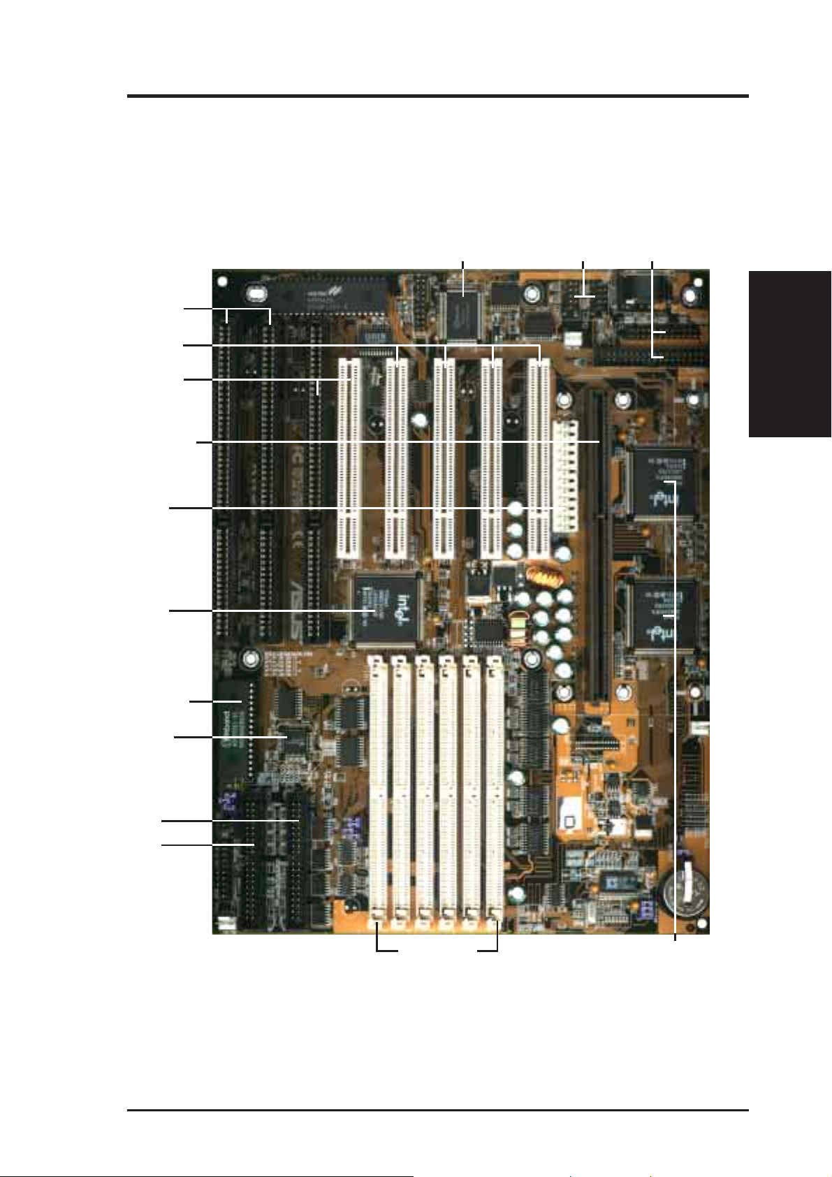
II. FEATURES
The ASUS KN97 Motherboard
2 ISA Slots
4 PCI Slots
ISA/PCI Slot
SEC CPU Slot
AT Power
Connector
Intel PIIX3
PCIset
Multi-I/O
Serial COM 1/2
Parallel/Floppy
II. FEATURES
(ASUS Board Parts)
Programmable
Flash ROM
Hardware
Monitor
(optional)
IDE 1
IDE 2
6 SIMM Sockets
Intel’s
440FX PCIset
ASUS KN97 User’s Manual 9
Page 10
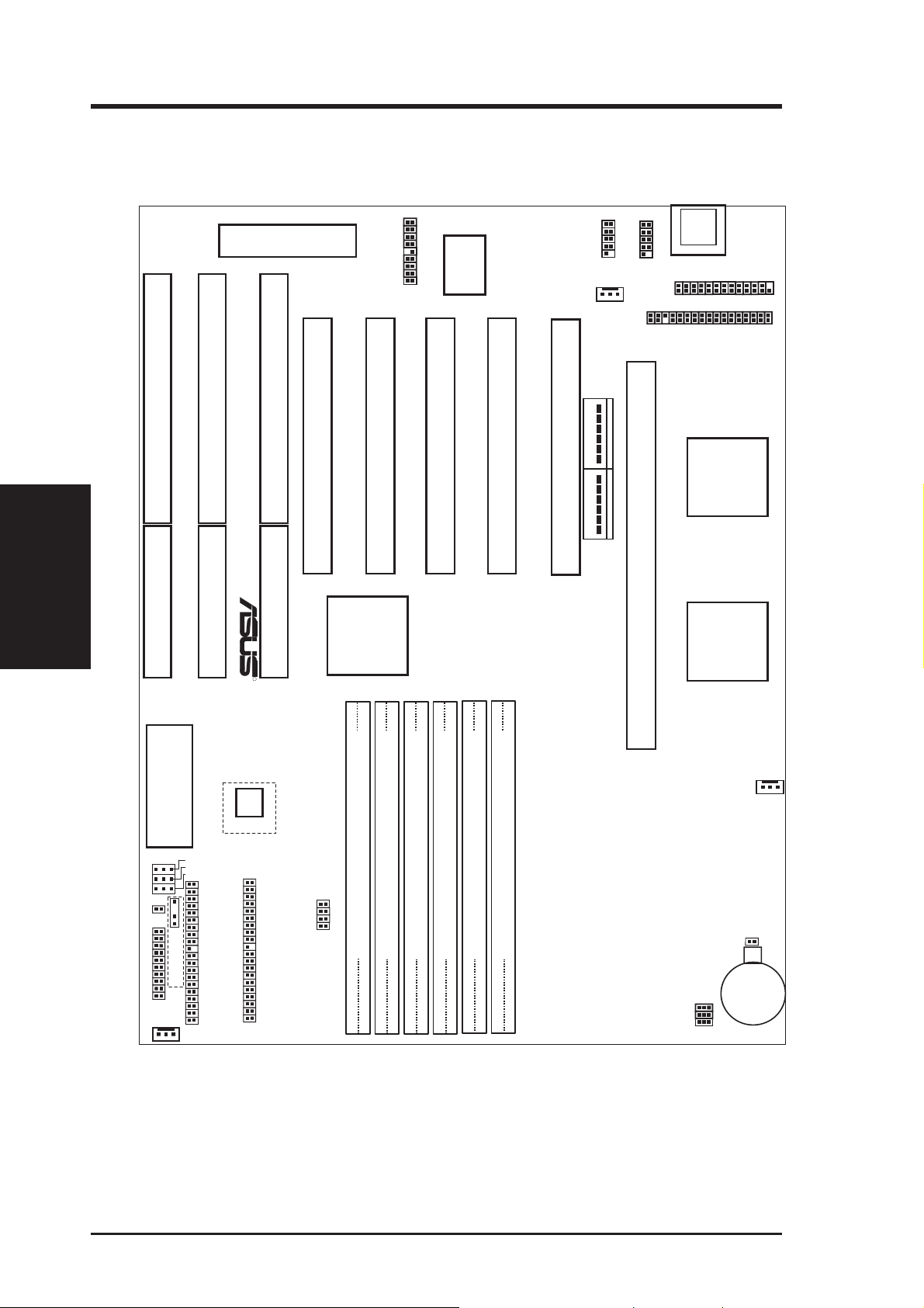
III. INSTALLATION
Layout of the ASUS KN97 Motherboard
COM 2
ISA Slot 3
Keyboard BIOS
ISA Slot 2
ISA Slot 1
USB, PS/2
Mouse, IrDA
Super
Multi-I/O
COM 1
Serial Ports
Power Fan
Keyboard
Parallel Port
III. INSTALLATION
(Board Layout)
Flash ROM
for BIOS
PCI Slot 5
PCI Slot 4
PCI Slot 3
PCI Slot 2
PCI Slot 1
Floppy Drives
Single Edge Contact (SEC) CPU Slot
AT Power Input
P9
Intel 440FX
P8
Intel PIIX3
PCIset
R
SIMM Socket 6 (32-bit, 72-pin module)
SIMM Socket 5 (32-bit, 72-pin module)
SIMM Socket 4 (32-bit, 72-pin module)
SIMM Socket 3 (32-bit, 72-pin module)
SIMM Socket 2 (32-bit, 72-pin module)
SIMM Socket 1 (32-bit, 72-pin module)
PCIset
Intel 440FX
PCIset
CPU Fan
LM78
Hardware
Monitor
Boot Block Write
Multi I/O En/Dis
RTC Clear
Secondary IDE
IDE LED
Panel Connectors
Chassis Connector
Chassis Fan
Primary IDE
FREQ.
RATIO
Row
BF0
BF1
BF2
BF3
BUS Freq.
FS2
FS1
01
01
23
23
45
45
FS0
Battery Test
BIOS Power
CR2032 3V
Lithium Cell
The items in outline are only available on motherboards with the LM78 Hardware Monitor
10 ASUS KN97 User’s Manual
Page 11

III. INSTALLATION
Jumpers
1) SIO p. 13 Onboard Multi-I/O Selection (En./Dis.)
2) BBLKW p. 13 Flash ROM Boot Block Programming (Protect/Prog.)
3) RTCLR p. 14 Real Time Clock (RTC) RAM (Keep/Clear CMOS)
4) BATTEST p. 14 Battery Test (Operation/Test Mode)
5) FS0, FS1, FS2 p. 15 CPU External Clock (BUS) Frequency Selection
6) BF0, BF1, BF2, BF3 p. 15 CPU to BUS Frequency Ratio
Expansion Slots/Sockets
1) System Memory p. 16 System Memory Support
2) SIMM Sockets p. 17 SIMM Memory Module Support
3) SEC CPU Slot p. 20 Single Edge Contact CPU Support
4) SLOT1, SLOT2, SLOT3 p. 25 16-bit ISA Bus Expansion Slots
5) PCI1, PCI2, PCI3, PCI4, PCI5 p. 25 32-bit PCI Bus Expansion Slots
Connectors
1) KB p. 27 Keyboard Connector (5-pin female)
2) PRINTER p. 27 Parallel (Printer) Port Connector (25-pin female)
3) FLOPPY p. 28 Floppy Drive Connector (34-pin Block)
4) PWR_F AN, CPU_FAN, CHA_F AN p. 28 Power Supply, CPU, Chassis Fan Power (3-pin block)
5) COM1, COM2 p. 29 Serial Port (Two 9-pin female)
6) PWRAT p. 29 AT Power Supply Connector (12-pin block)
7) IDE1, IDE2 p. 30 Primary / Secondary IDE Connector (40-pin blocks)
8) IDELED p. 30 IDE LED Activity Light
9) TB LED (PANEL) p. 31 System Power LED (2 pins)
10) SMI (PANEL) p. 31 SMI Switch Lead (2 pins)
11) RESET (PANEL) p. 31 Reset Switch Lead (2 pins)
12) KEYLOCK (P ANEL) p. 31 Power LED (3 pins) & Keyboard Lock Switch (2 pins)
13) SPEAKER (PANEL) p. 31 Speaker Output Connector (4 pins)
14) CHASSIS (optional) p. 32 Chassis Open Alarm Lead (3-pin Block)
15) USBIRMOUSE p. 32 Universal Serial BUS Ports 1 & 2 (Two 4-pin female)
*
†
(Board Layout)
III. INSTALLATION
*
The onboard hardware monitor uses the I/O address 290H-297H so legacy ISA cards must
not use this I/O address or else conflicts will occur.
†
PCI slots 4&5 share the same interrupt number (INT#) so PCI cards on these two slots must be
able to share an INT# or make sure that one of these PCI cards does not use an INT#.
ASUS KN97 User’s Manual 11
Page 12
III. INSTALLATION
Installation Steps
Before using your computer, you must complete the following steps:
1. Set Jumpers on the Motherboard
2. Install DRAM Modules
3. Install the Central Processing Unit (CPU)
4. Install Expansion Cards
5. Connect Ribbon Cables, Cabinet Wires, and Power Supply
6. Setup the BIOS Software
1. Jumpers
Several hardware settings are made through the use of jumper caps to connect jumper
pins (JP) on the motherboard. See “Map of the Motherboard” on page 4 for locations
III. INSTALLATION
(Jumpers)
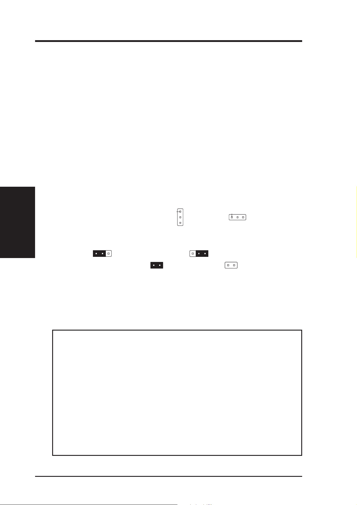
of jumpers. The jumper settings will be described numerically such as [----], [1-2],
[2-3] for no connection, connect pins 1&2, and connect pins 2&3 respectively . Pin 1
Pin 1
for our motherboards is always on top
motherboard with the keyboard connector away from yourself. A “1” is written
besides pin 1 on jumpers with three pins. The jumpers will also be shown graphically such as
with two pins will be shown as
manufacturing simplicity, the jumpers may be sharing pins from other groups. Use
the diagrams in this manual instead of following the pin layout on the board. Settings
with two jumper numbers require that both jumpers be moved together. To connect
the pins, simply place a plastic jumper cap over the two pins as diagramed.
WARNING! Computer motherboards, baseboards and components, such as SCSI
cards, contain very delicate Integrated Circuit (IC) chips. To protect them against
damage from static electricity , you should follow some precautions whenever you
work on your computer.
to connect pins 1&2 and to connect pins 2&3. Jumpers
for Short (On) and for Open (Off). For
or on the left
Pin 1
when holding the
1. Unplug your computer when working on the inside.
2. Use a grounded wrist strap before handling computer components. If you do
not have one, touch both of your hands to a safely grounded object or to a
metal object, such as the power supply case.
3. Hold components by the edges and try not to touch the IC chips, leads or
connectors, or other components.
4. Place components on a grounded antistatic pad or on the bag that came with
the component whenever the components are separated from the system.
12 ASUS KN97 User’s Manual
Page 13
III. INSTALLATION
Jumper Settings
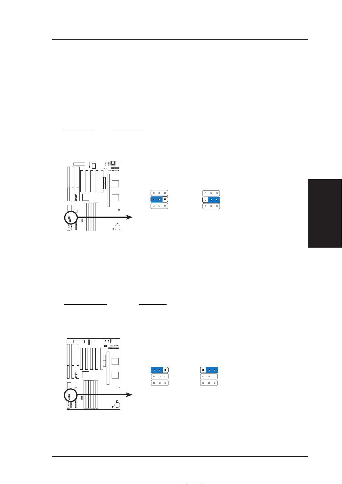
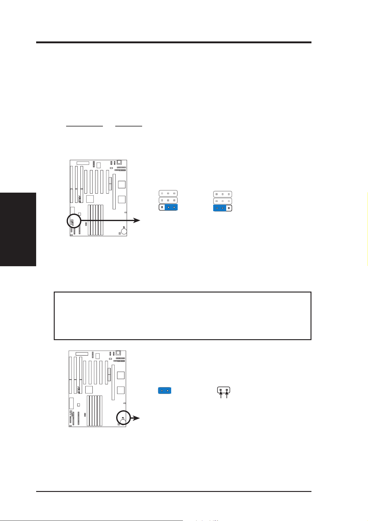
1. Onboard Multi-I/O Selection (SIO)
Y ou can selectively disable each onboard multi-I/O item (floppy, serial, parallel,
and IrDA) through the Chipset Features Setup under BIOS SOFTWARE or
disable all multi-I/O items at once with the following jumper so you can use
your own multi-I/O card.
Multi-I/O SIO: M/IO
Enable [1-2] (Default)
Disable [2-3]
123
R
Enable
(Default)
SIO
123
SIO
Disable
2. Flash ROM Boot Block Programming (BBLKW)
This sets the operation mode of the boot block area of the Programmable Flash
ROM to allow programming in the Program position. This is required only if
prompted by the Flash Memory Writer Utility as shown in BIOS SOFTW ARE.
Programming BBLKW
Protect [1-2] (Default)
Program [2-3]
(Jumpers)
III. INSTALLATION
123
BBLKW
R
Protect
(Default)
123
BBLKW
Program
ASUS KN97 User’s Manual 13
Page 14
III. INSTALLATION
3. Real Time Clock (RTC) RAM (RTCLR)
The CMOS RAM is powered by the onboard button cell battery. To clear the
R TC data: (1) T urn off your computer and unplug your AC power, (2) Move this
jumper to “Clear CMOS,” (3) Move the jumper back to “Keep,” (4) Turn on
your computer, (5) Hold down <Delete> during bootup and enter BIOS setup to
re-enter user preferences.
RTC RAM RTCLR
Keep CMOS [2-3] (Default)
Clear CMOS [1-2] (momentarily)
III. INSTALLATION
(Jumpers)
123
R
RTCLR
Keep CMOS
(Default)
123
RTCLR
Clear CMOS
4. Battery T est (BATTEST)
You can test the battery’s current by removing this jumper and attaching a current meter the two pins.
WARNING! You must unplug the power cord to your power supply to ensure that
there is no power to your motherboard. The CMOS RAM containing BIOS setup
information may be cleared by this action. You should enter BIOS to “Load Setup
Defaults” and re-enter any user information after removing and reapplying this jumper .
BATTEST
Battery Test
R
Battery Test
BATTEST
Operation
(Default)
14 ASUS KN97 User’s Manual
Page 15
III. INSTALLATION
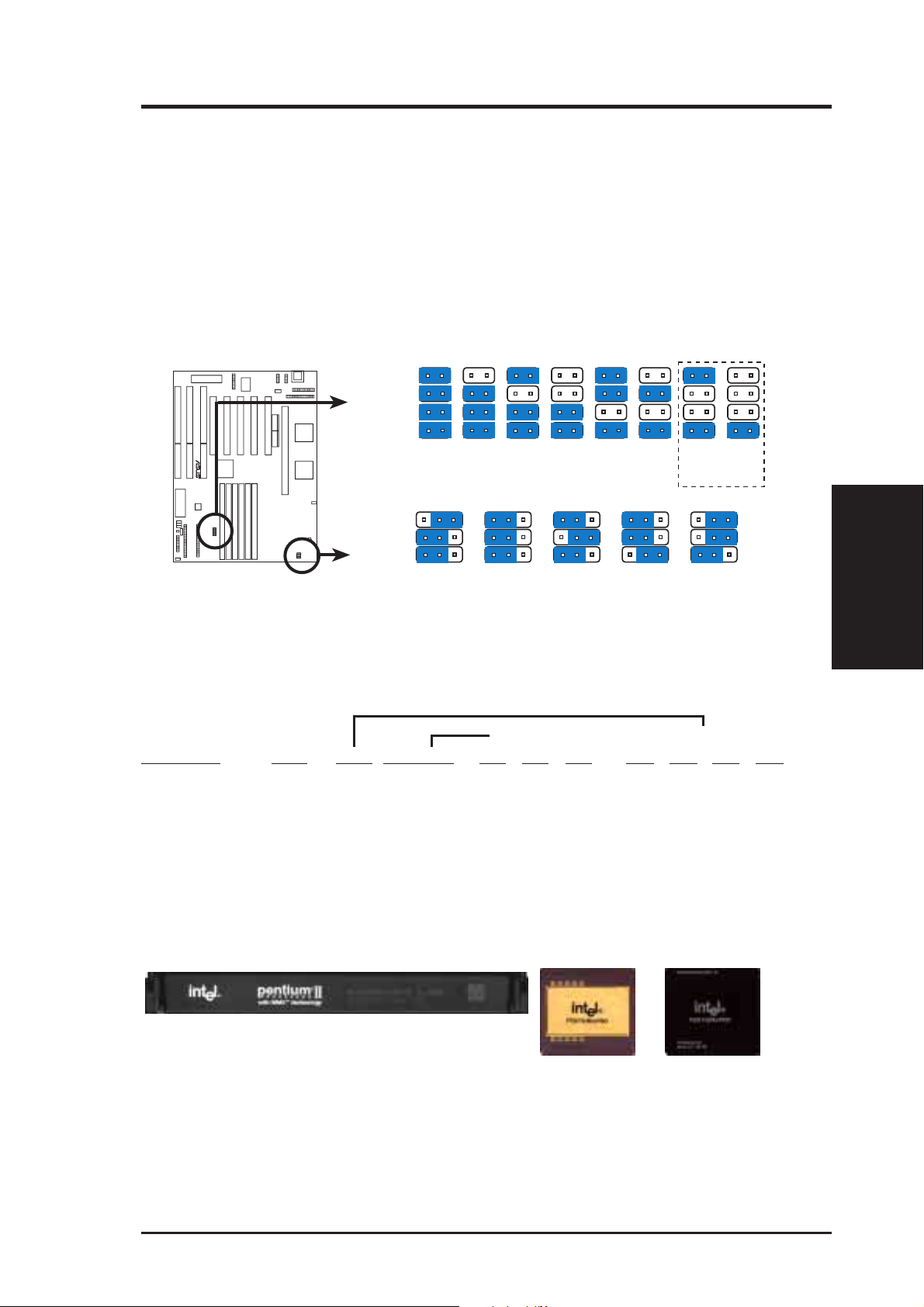
5. CPU External Clock (BUS) Frequency Selection (FS0, FS1, FS2)
These jumpers tell the clock generator what frequency to send to the CPU. These
allow the selection of the CPUs External frequency (or BUS Clock). The BUS Clock
times the BUS Ratio equals the CPUs Internal frequency (the advertised CPU speed).
6. CPU to BUS Frequency Ratio (BF0, BF1, BF2, BF3)
These jumpers set the frequency ratio between the Internal frequency of the CPU
and the External frequency (called the BUS Clock) within the CPU. These must
be set together with the above jumpers CPU External (BUS) Frequency Selection.
BF0
BF1
BF2
BF3
3.5x
4.0x
3.0x2.5x2.0x 5.0x
R
CPU : BUS Frequency Ratio
4.5x
5.5x
Reserved for
future CPUs
123
FS2
FS1
FS0
60MHz
CPU External Clock (BUS) Frequency Selection
123
66MHz
123
68MHz
123
75MHz
123
83MHz
WARNING! 68MHz, 75MHz, and 83MHz frequencies exceed the specifications
for the onboard Intel Chipset and are not guaranteed to be stable.
Set the jumpers by the internal speed of your processor as follows:
(BUS Freq.) (Freq. Ratio)
CPU Model Freq. Ratio BUS Freq. FS2 FS1 FS0 BF0 BF1 BF2 BF3
[Reserved] 333MHz 5.0x 66MHz [1-2] [1-2] [1-2] [on] [off] [off] [on]
Intel Pentium II 300MHz 4.5x 66MHz [1-2] [1-2] [1-2] [off] [on] [off] [on]
Intel Pentium II 266MHz 4.0x 66MHz [1-2] [1-2] [1-2] [on] [on] [off] [on]
Intel Pentium II 233MHz 3.5x 66MHz [1-2] [1-2] [1-2] [off] [off] [on] [on]
Pentium Pro 200MHz 3.0x 66MHz [1-2] [1-2] [1-2] [on] [off] [on] [on]
Pentium Pro 180MHz 3.0x 60MHz [2-3] [1-2] [1-2] [on] [off] [on] [on]
Pentium Pro 166MHz 2.5x 66MHz [1-2] [1-2] [1-2] [off] [on] [on] [on]
Pentium Pro 150MHz 2.5x 60MHz [2-3] [1-2] [1-2] [off] [on] [on] [on]
(Jumpers)
III. INSTALLATION
Intel Pentium II Processor in a SEC Cartridge
(233-333MHz 256/512KB L2 Cache)
Intel Pentium Pro Processor
(150-200MHz 256/512/1,024KB L2 Cache)
NOTE: Voltage Regulator Output Selection (VID) is not needed for the Pentium II
and Pentium Pro processors because these CPUs send a VID signal directly to the
onboard power controller.
ASUS KN97 User’s Manual 15
Page 16
2. System Memory (SIMM)
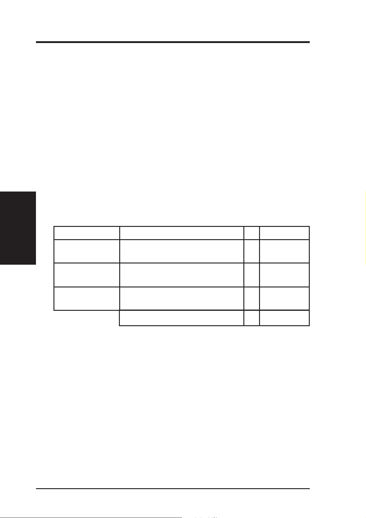
This motherboard supports six 72-pin SIMMs (Single Inline Memory Modules) of
4MB, 8MB, 16MB, 32MB, 64MB to form a memory size between 8MB to 384MB.
The SIMMs can be either 60ns or 70ns Fast Page Mode (Asymmetric or Symmetric), Extended Data Output (EDO) (Burst Extended Data Output or BEDO and parity are not supported). To support ECC, you must use true (as opposed to phantom
parity generated by TTL chips) 36-bit parity-type SIMM (e.g. 8 chips + 4 parity
chips) in pairs for all modules. Mixing 32-bit non-parity SIMM (e.g., 8 chips) and
36-bit SIMM (e.g., 12 chips) will work minus the ECC feature.
IMPORTANT: Memory setup is required through “Auto Configuration” in the
CHIPSET FEATURES SETUP of Section IV, BIOS software. Each bank must
have the same size memory installed in pairs. Do not use memory modules with
III. INSTALLATION
(System Memory)
more than 24 chips per module. Modules with more than 24 chips exceed the design
specifications of the memory subsystem and will be unstable.
Install memory in any or all of the banks in any combination as follows:
Memory Slots SIMM Memory Module Total Memory
SIMM Slots 1 & 2 4MB, 8MB, 16MB, 32MB, 64MB x2
(Bank0) 72-pin FPM or EDO SIMM
SIMM Slots 3 & 4 4MB, 8MB, 16MB, 32MB, 64MB x2
(Bank1) 72-pin FPM or EDO SIMM
SIMM Slots 5 & 6 4MB, 8MB, 16MB, 32MB, 64MB x2
(Bank2) 72-pin FPM or EDO SIMM
Total System Memory (Max 384MB) =
16 ASUS KN97 User’s Manual
Page 17
III. INSTALLATION
SIMM Memory Installation
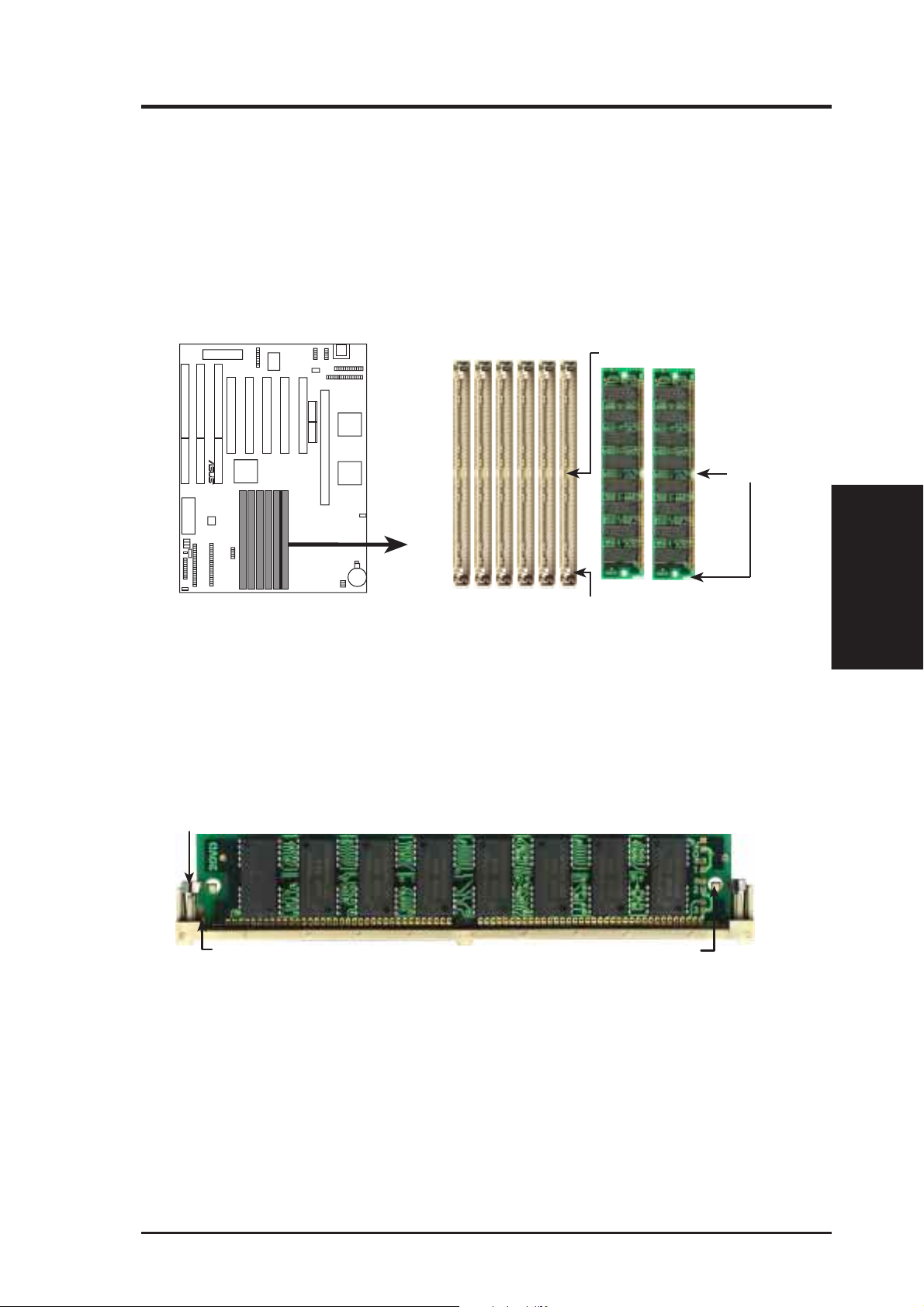
1. The SIMM memory modules will only fit one way as shown. The central notch
of the module must be aligned with the rib midway inside the slot while the
other notch at one end of the module must be aligned with the plastic safety tab
on the slot.
123456
R
Rib (inside slot)
Notch
Safety tab
72-Pin SIMM Sockets
2. Push the memory module gently but firmly into place starting from a 45-degree
angle making sure that all the contacts are aligned with the socket.
3. With your fingertips (pointer) on the slot’ s clips and your thumbs holding down
its top edges, push the SIMM into a vertical position so that it clicks into place.
(System Memory)
III. INSTALLATION
Support Clip
Safety Tab (This Side Only)
72 Pin DRAM in SIMM Socket
Mounting Hole
4. The plastic guides must go through the two mounting holes on the SIMM’s
sides.
5. If you need to remove one or more memory modules, remove them by pushing
the clips outward. The SIMM will be released from its slot, and you can pull the
SIMM straight up and out of the slot.
ASUS KN97 User’s Manual 17
Page 18
III. INSTALLATION
III. INSTALLATION
3. Central Processing Unit (CPU)
The ASUS KN97 motherboard provides a Single Edge Contact (SEC) slot for a
Pentium II processor packaged in an SEC cartridge (pages 18–22) or a Pentium Pro
processor installed in the ASUS C-P6SI Pentium Pro SEC Card (pages 23–24).
Pentium II Processor
WARNING! Be sure that sufficient air circulation is available across the processor’ s pas-
sive heatsink. W ithout sufficient circulation, the processor could overheat and damage both
the processor and the motherboard. You may install an auxiliary fan, if necessary .
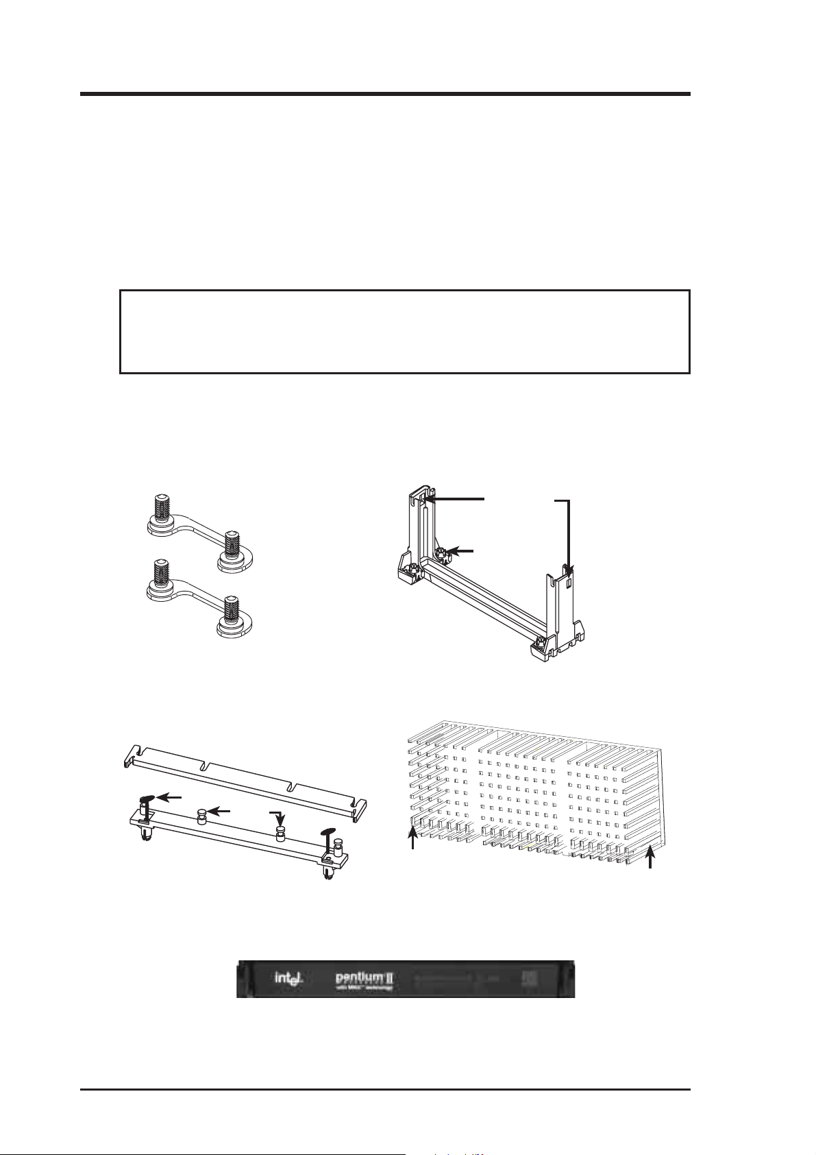
You should check to see that you have the following 9 items. (NOTE: The pictures
in the following pages will have the same item numbers next to them for your reference. The design and color of your items may be slightly different.)
(CPU)
(1)
(2)
Attach Mount Bridges (Items 1,2)
(Factory Installed)
Top Bar (4)
(5)
Heatsink Support Base/Top Bar (Items 4-7)
Pin
Posts
(6)
Base (7)
Lock Holes
Captive Nut
(3)
Pentium II Retention Mechanism (Item 3)
(8)
Larger Fin should
be on the bottom.
Pentium II Processor Heatsink (Item 8)
Heatsink bottom Groove
for the Support Top Bar
Intel Pentium II Processor in a SEC Cartridge
(233-333MHz 256/512KB L2 Cache)
CPU (Item 9)
18 ASUS KN97 User’s Manual
Page 19
III. INSTALLATION
The ASUS KN97 As Shipped
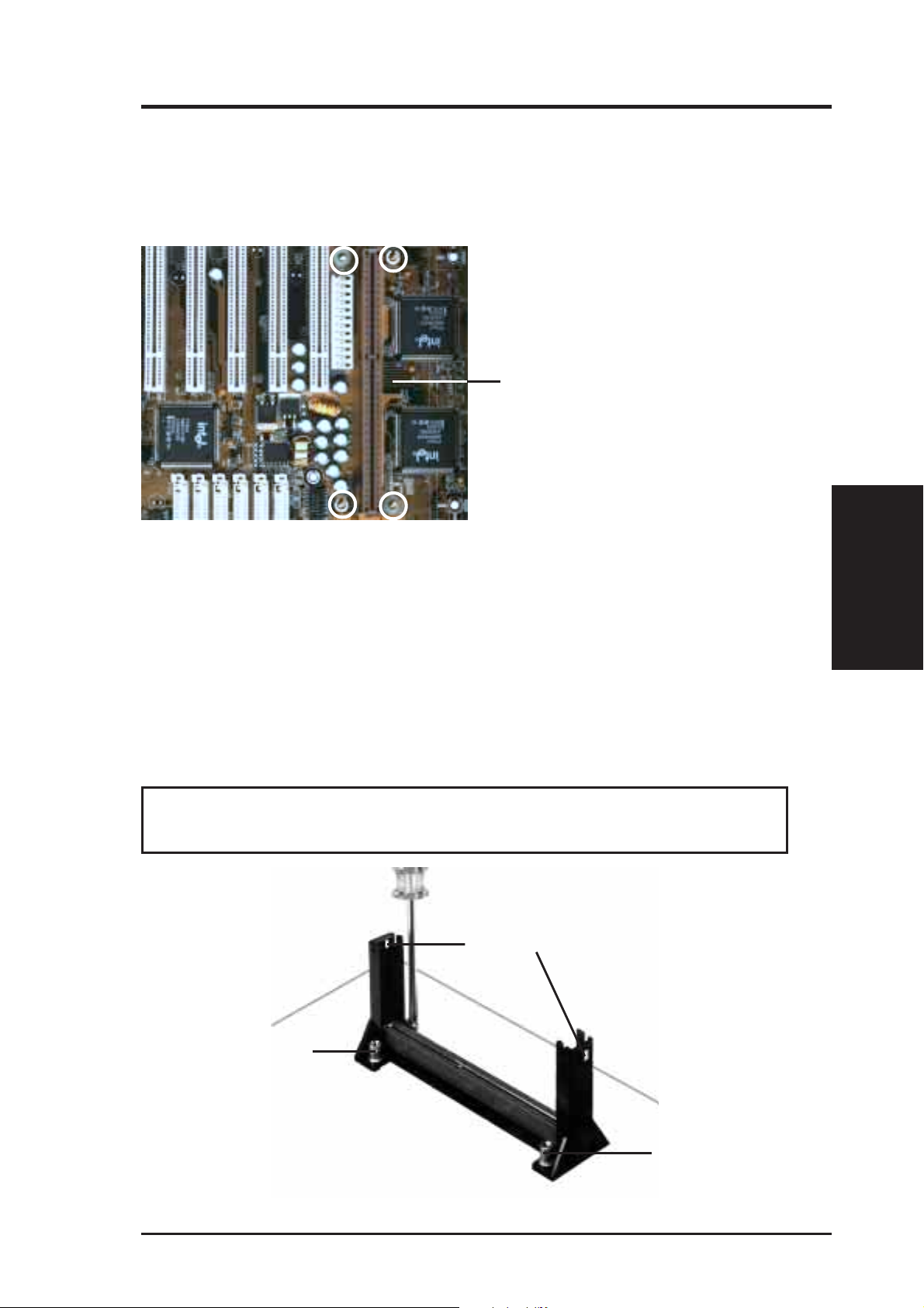
Four screws should be showing next to each corner of the SEC CPU Slot using two
attach mount bridges from the underside of the motherboard. A bottom heatsink
support base must be mounted over the two chipsets located to the side of the slot.
NOTE: Encircled items are screws from
the mount bridges (1 & 2)
SEC CPU slot
Installing the Pentium II Processor:
1. Mount the Pentium II Retention Mechanism: The retention mechanism is
designed to fit into the SEC slot only one way.
TIP: Orient the mechanism’s lock holes toward the motherboard’s chipsets (see
motherboard layout for the location of the Intel 440FXPCIset).
Be sure to align the notch in the mechanism with the small rib on one side of the
slot. Screw the captive nuts in place
WARNING! Do not overtighten the captive nuts. Doing so could damage your
motherboard. Tighten captive nuts to no more than 6±1 inch/pound.
Lock holes
(CPU)
III. INSTALLATION
Captive nut
Captive nut
ASUS KN97 User’s Manual 19
Page 20
III. INSTALLATION
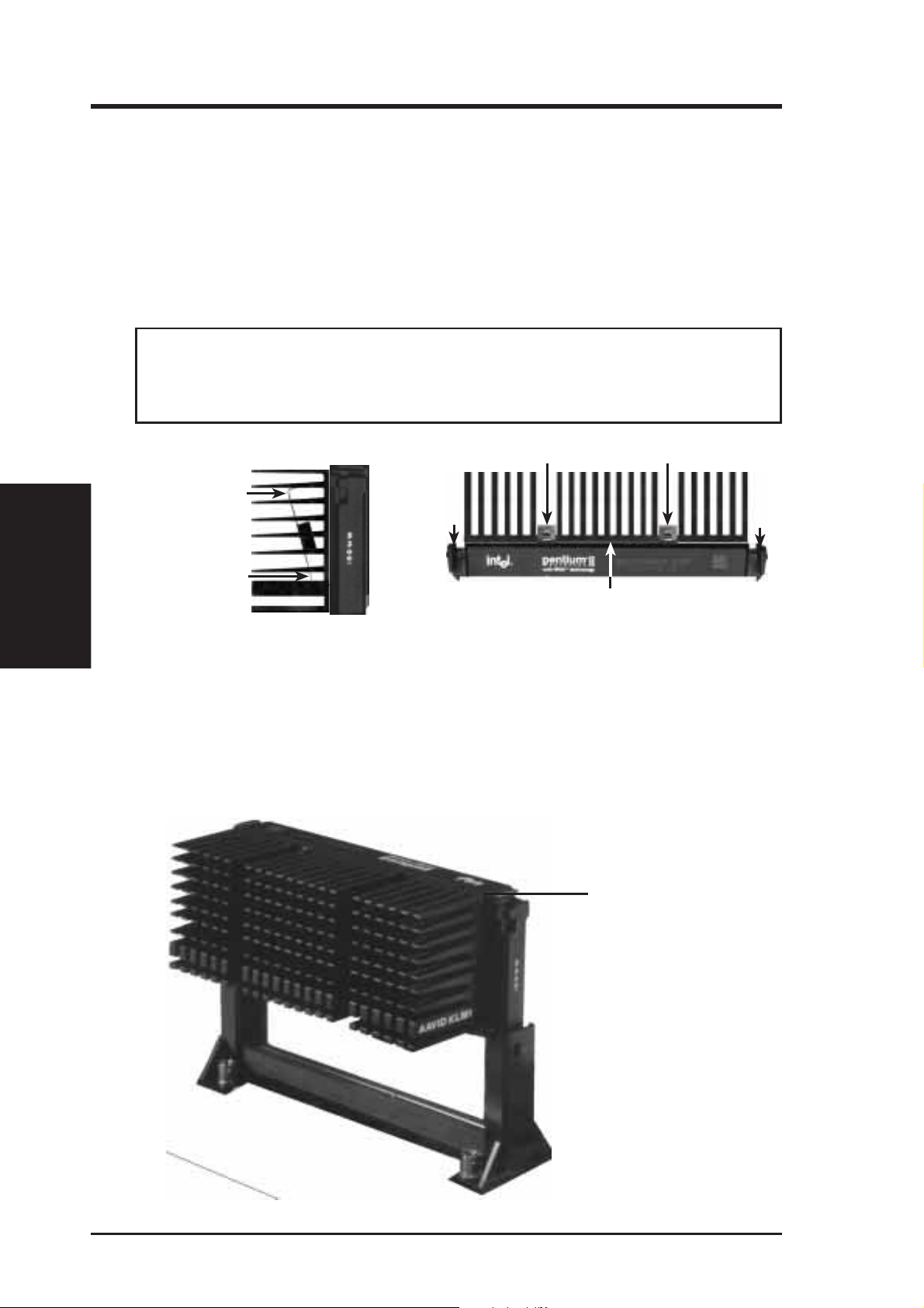
2. Mount the Heatsink: Place the SEC cartridge face down on a flat surface and lay
the heat sink flush on the back (metal side) of the SEC cartridge. Check the orientation of the heatsink against the pictures. The thicker fin must be orientated
toward the bottom. The top clamp is wider than the bottom clamp so only this
orientation will fit. With a screw driver, push the clamps one at a time into the
SEC cartridge. Be sure that the heatsink is firmly pressed against the SEC cartridge. When correctly installed, no light must be showing through between the
thermal pad of the heatsink and the SEC cartridge.
WARNING! If the heatsink is not mounted tightly against the SEC cartridge,
the CPU will overheat. You may install an auxiliary fan to provide adequate
circulation across the processor’s passive heatsink.
III. INSTALLATION
(CPU)
(8)
Push Clamp
Push Clamp
SEC Cartridge with Heatsink (Side View)
(9)
Push each end of the clamps until they lock
Lock
The thermal pad & SEC cartridge should not have a gap!
SEC Cartridge with Heatsink (Top View)
(8)
Lock
(9)
3. Insert the SEC Cartridge: Push the SEC cartridge’s two locks inward (the
preceding picture shows the locks in the outward position and inward in the
picture below). With the heatsink facing the motherboard’s chipsets, press the
cartridge gently but firmly until it is full inserted.
(8)
Push lock inward
(3)
20 ASUS KN97 User’s Manual
Page 21
III. INSTALLATION
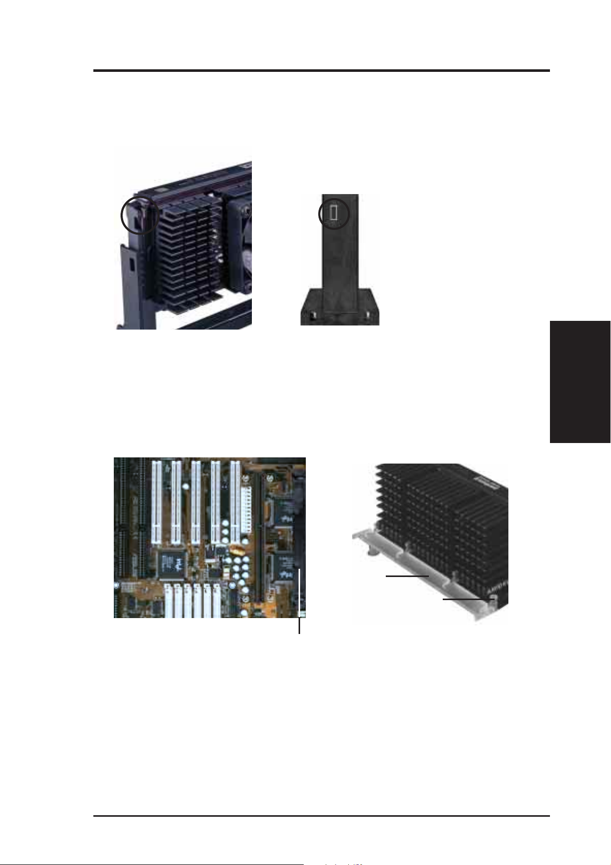
4. Secure the SEC Cartridge: Secure the SEC cartridge in place by pushing the
SEC cartridge locks outward so that the lock shows through the retention
mechanism’s lock holes.
(3)
(3)
(8)
5. Secure the Heatsink: Install the heatsink support base into the motherboard.
This is not, however, necessary if you use a heatsink with fan (see next page).
The support base is necessary to secure the heatsink (without fan). Secure the
heatsink by sliding the heatsink support top bar into the bottom groove of the
heatsink until it locks into the heatsink support base posts.
(CPU)
III. INSTALLATION
(8)
Heatsink support
top bar (4)
Heatsink support
base post
Heatsink support
base (7)
(9)
6. Set Jumpers: Refer to jumper settings for “CPU to BUS Frequency Ratio” and
jumpers for “BUS Frequency Selection” if you haven’t set them yet.
ASUS KN97 User’s Manual 21
Page 22
III. INSTALLATION
III. INSTALLATION
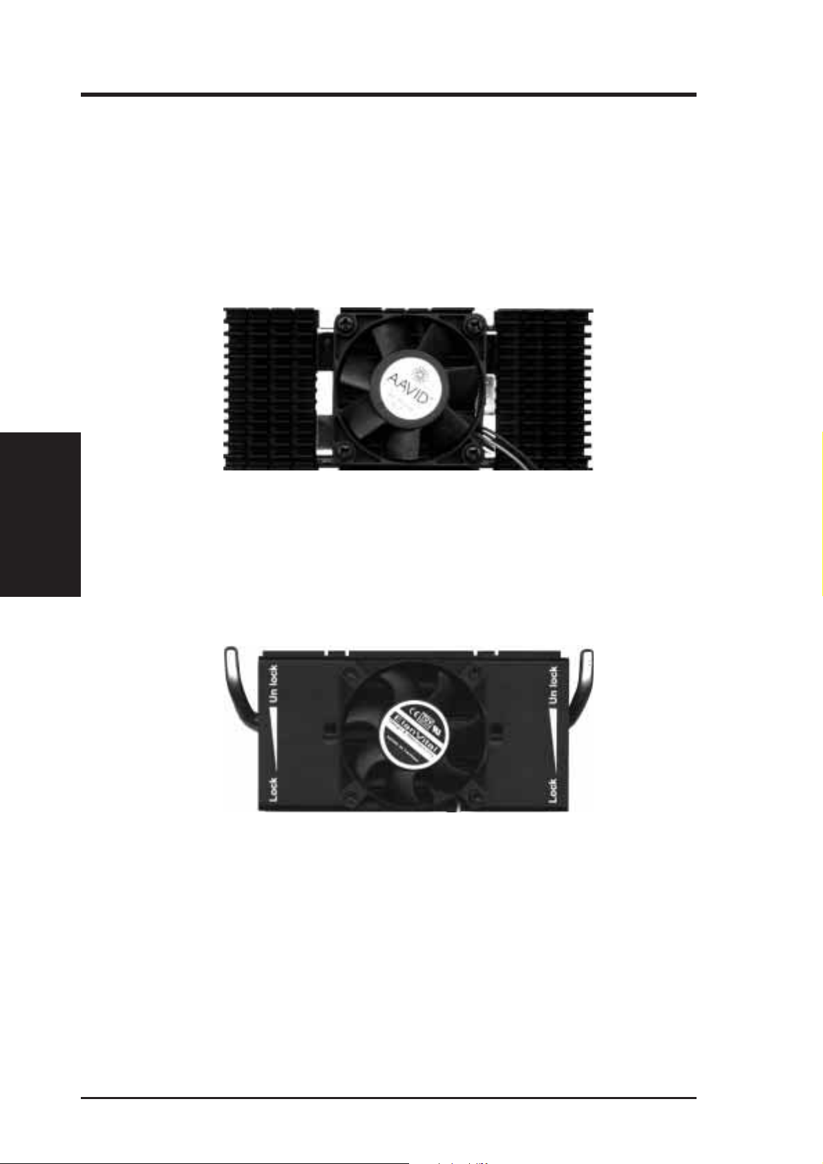
The heatsinks shown in this manual are for reference purposes only. The recommended heatsinks for the Pentium II processor are those with three-pin fans that can
be connected to the CPU fan connector on motherboard. These heatsinks have the
added benefits of proper heat dissipation and with the LM78 hardware monitor, the
ability to monitor the fan’s RPM and use the alert function through the included
LANDesk Client Manager (LDCM) software.
AAVID Heatsink
(CPU)
The procedures for installing the AAVID heatsink with fan is similar as that for the
heatsink without a fan. You will not, however, be able to use the heatsink support top
bar because of the fan. The heatsink support top bar will, however , still be included
in the package, in case you use a heatsink without a fan.
Elan Vital Heatsink
The procedures for installing the Elan V ital heatsink with fan is also similar as that for
the heatsink without a fan. The Elan Vital heatsink, however, comes with a lever to
clamp the heatsink into the SEC cartridge. Mount the heatsink in the orientation as
shown then flip the lever from “Unlock” to “Lock.” You will not be able to also use the
heatsink support top bar because of the fan. The heatsink support top bar will, however, still be included in the package, in case you use a heatsink without a fan.
22 ASUS KN97 User’s Manual
Page 23
III. INSTALLATION
Pentium Pro SEC Card
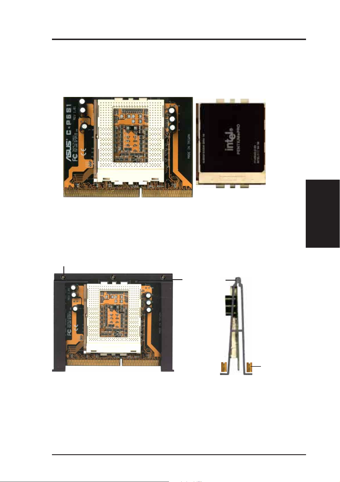
The C-P6S1 Pentium Pro SEC Card allows you to interface a 387-pin ZIF Socket 8
onto your Pentium II Slot so that Pentium Pro processors can be used on Pentium II
motherboards.
Installing the Pentium Pro Processor
1. Mount the Metal Support Frame: Place the Metal Support Frame over the C-
P6S1 Pentium Pro SEC Card as shown and tighten the three support frame screws,
if necessary.
3 Support Frame Screw Holes
Metal Support Frame
Front View
Side View
4 Captive Nuts
(CPU)
III. INSTALLATION
ASUS KN97 User’s Manual 23
Page 24
III. INSTALLATION
III. INSTALLATION
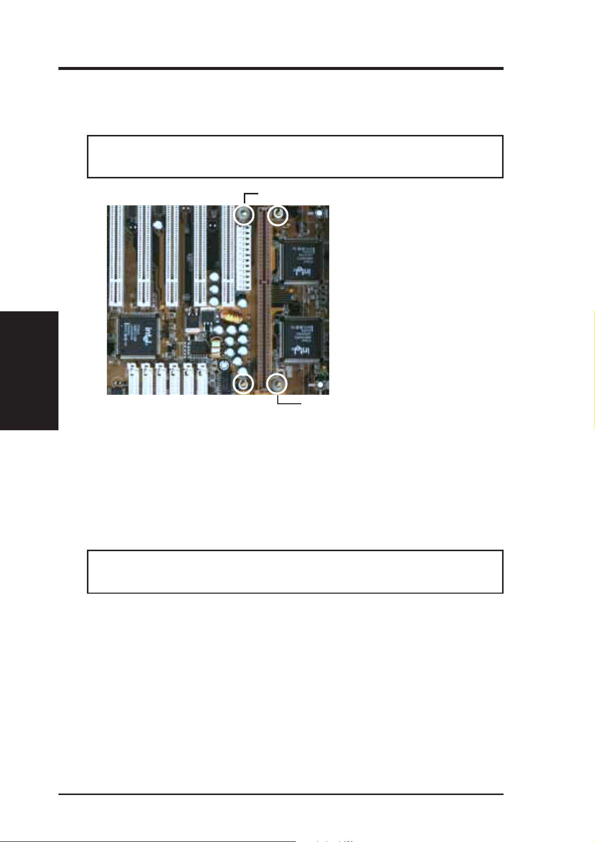
2. Secure the SEC Card: Place the four plastic washers over the mount bridge
screws (encircled) and secure the C-P6S1 Pentium Pro SEC Card using the four
captive nuts.
WARNING! Do not overtighten the captive nuts. Doing so could damage your
motherboard. Tighten captive nuts to no more than 6±1 inch/pound.
With washer
(CPU)
With washer
3. Install the Processor: Install a Pentium Pro processor with a heatsink and fan.
To install the processor, open the ZIF socket by first pulling the lever sideways
away from the socket’s “Lock” then upwards to a 90-degree right angle. Insert the
CPU with the correct orientation. Look to see that the pins are more dense on one
half compared to the other half. W ith the added weight of the CPU fan, no force is
required to insert the CPU. Once completely inserted, hold down on the fan and
close the socket’s lever.
WARNING! Without a fan, the CPU can overheat and cause damage to both the
CPU and the motherboard.
4. Set Jumpers: Refer to jumper settings for “CPU to BUS Frequency Ratio” and
jumpers for “BUS Frequency Selection” if you haven’t set them yet.
24 ASUS KN97 User’s Manual
Page 25

III. INSTALLATION
4. Expansion Cards
WARNING! Unplug your power supply when adding or removing expansion
cards or other system components. Failure to do so may cause severe damage to
both your motherboard and expansion cards.
First read your expansion card documentation for hardware and software settings
that may be required to set up your specific card.
Expansion Card Installation Procedure
1. Read the documentation for your expansion card.
2. Set any necessary jumpers on your expansion card.
3. Remove your computer system’s cover.
4. Remove the bracket on the slot you intend to use. Keep the bracket for possible
future use.
5. Carefully align the card’s connectors and press firmly.
6. Secure the card on the slot with the screw you removed in step 4.
7. Replace the computer system’s cover.
8. Set up the BIOS if necessary (such as IRQ xx Used By ISA: Yes in PNP AND
PCI SETUP)
9. Install the necessary software drivers for your expansion card.
Assigning IRQs for Expansion Cards
Some expansion cards need to use an IRQ to operate. Generally an IRQ must be
exclusively assigned to one use. In a standard design there are 16 IRQs available but
most of them are already in use, leaving 6 IRQs free for expansion cards.
Both ISA and PCI expansion cards may require to use IRQs. System IRQs are available to cards installed in the ISA expansion bus first, then any remaining IRQs are
available to PCI cards. Currently , there are two types of ISA cards. The original ISA
expansion card design, now referred to as legacy ISA cards, requires that you configure the card’ s jumpers manually and then install it in any available slot on the ISA
bus. You may use Microsoft Diagnostics (MSD.EXE) utility located in the Windows directory to see a map of your used and free IRQs. If you use W indows 95, the
Resources tab under Device Manager displays the resource settings being used by
a particular device (to gain access, double-click the System icon under the Control
Panel program). Ensure that no two devices share the same IRQs or your computer
will experience problems when those two devices are in use at the same time.
(Expansion Cards)
III. INSTALLATION
ASUS KN97 User’s Manual 25
Page 26

To simplify this process, this motherboard complies with the Plug and Play (PnP)
specification, which was developed to allow automatic system configuration whenever a PnP-compliant card is added to the system. For PnP cards, IRQs are assigned
automatically from those available.
If the system has both legacy and PnP ISA cards installed, IRQs are assigned to PnP
cards from those not used by legacy cards. The PCI and PNP configuration section
of the BIOS setup utility can be used to assign which IRQs are being used by legacy
cards. For older legacy cards that do not work with the BIOS, you may contact your
vendor for an ISA Configuration Utility.
An IRQ number is automatically assigned to PCI expansion cards after those used
by legacy and PnP ISA cards. In the PCI bus design, the BIOS automatically assigns
an IRQ to a PCI slot that contains a card requiring an IRQ. T o install a PCI card, you
need to set the INT (interrupt) assignment. Since all the PCI slots on this mother-
III. INSTALLATION
(DMA Channels)
board use an INTA #, set the jumpers on your PCI cards to INT A.
III. INSTALLATION
Assigning DMA Channels for ISA Cards
Some ISA cards, both legacy and PnP, may also need to use a DMA (Direct Memory
Access) channel. DMA assignments for this motherboard are handled the same way
as the IRQ assignment process described earlier. You can select a DMA channel in
the PCI and PnP configuration section of the BIOS Setup utility.
IMPORTANT: T o avoid conflicts, reserve the necessary IRQs and DMAs for legacy
ISA cards (under PNP AND PCI SETUP of the BIOS SOFTWARE, choose Yes in
IRQ xx Used By ISA and DMA x Used By ISA for those IRQs and DMAs you want to
reserve).
ISA Cards and Hardware Monitor
The onboard hardware monitor uses the I/O address 290H-297H so legacy ISA cards
must not use this I/O address otherwise conflicts will occur.
26 ASUS KN97 User’s Manual
Page 27
III. INSTALLATION
5. External Connectors
WARNING! Some pins are used for connectors or power sources. These are
clearly differentiated from jumpers as shown in the baseboard layout on page 10.
Placing jumper caps over these pins will cause damage to your baseboard.
IMPORTANT: Connect ribbon cables such that the red stripe is on the pin 1 side of
the connector. The four corners of the connectors are labeled on the baseboard. Pin
1 is the side closest to the power connector on hard and floppy disk drives. IDE
ribbon cable must be less than 18in. (46cm), with the second drive connector no
more than 6in. (15cm) from the first connector.
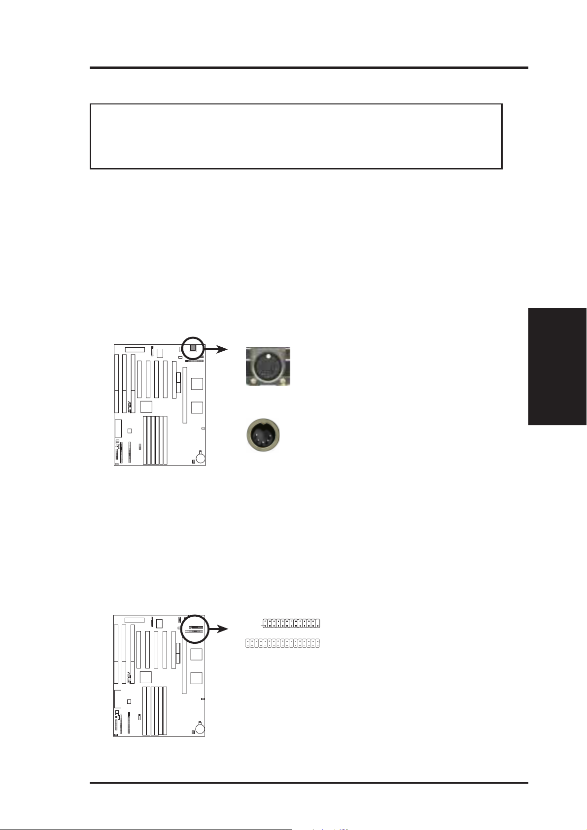
1. Keyboard Connector (KB )
This 5-pin female connector is for either a standard IBM-compatible, 101/102-
key, or 104-key (Windows 95-compatible) keyboard.
Onboard Keyboard Connector
(5-pin female)
R
This motherboard accepts
a 5-pin AT Keyboard Connector
2. Parallel Printer Connector (PRINTER)
This 26-pin block connector supports the included parallel port ribbon cable
with mounting bracket. Connect the ribbon cable to this connector and mount
the bracket to the case on an open slot. You can make available the parallel port
and choose the IRQ Onboard Parallel Port in Chipset Features of the BIOS
SOFTWARE. (Pin 26 is removed to prevent inserting in the wrong orienta-
tion when using ribbon cables with pin 26 plugged)
Pin 1
Orientate the floppy ribbon cable’s
red stripe to the connector’s Pin 1.
(Connectors)
III. INSTALLATION
For this connector to be available, you must connect
R
Parallel (Printer) Connector
the included Parallel (25-Pin female) cable set to a
free expansion slot opening.
TIP: You may also remove the bracket
connectors and mount them directly to
the case to save expansion slot space.
ASUS KN97 User’s Manual 27
Page 28
III. INSTALLATION
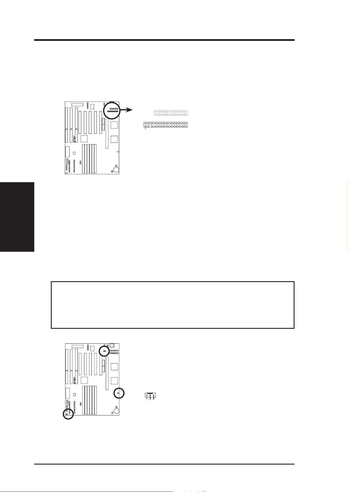
3. Floppy Disk Drive Connector (FLOPPY )
This 34-pin block connector supports the provided floppy drive ribbon cable.
After connecting the single end to the board, connect the two plugs on the other
end to the floppy drives. (Pin 5 is removed to prevent inserting in the wr ong
orientation when using ribbon cables with pin 5 plugged).
Orientate the floppy ribbon cable’s
red stripe to the connector’s Pin 1.
Pin 1
R
III. INSTALLATION
(Connectors)
Floppy Drive Connector
4. Power Supply, CPU Fan Connectors (FAN)
These connectors support cooling fans of 500mAmp (6watts) or less. Orientate
the fans so that the heat sink fins allow airflow to go across the onboard heat
sink(s) instead of the expansion slots. Depending on the fan manufacturer, the
wiring and plug may be different. The red wire should be positive, while the
black should be ground. Connect the fan’ s plug to the board taking into consideration the polarity of the this connector . NOTE: The “Rotation” signal is to
be used only by a specially designed fan with rotation signal.
WARNING! The CPU and/or motherboard will overheat if there is no airflow
across the CPU and heatsinks. Damage may occur to the motherboard and/or the
CPU fan if these pins are incorrectly used. These are not jumpers, do not
place jumper caps over these pins.
Power Supply Fan Power
R
12Volt CPU Fan Power
Chassis Fan Power
Ground
+12 Volt
Rotation
28 ASUS KN97 User’s Manual
Page 29
III. INSTALLATION
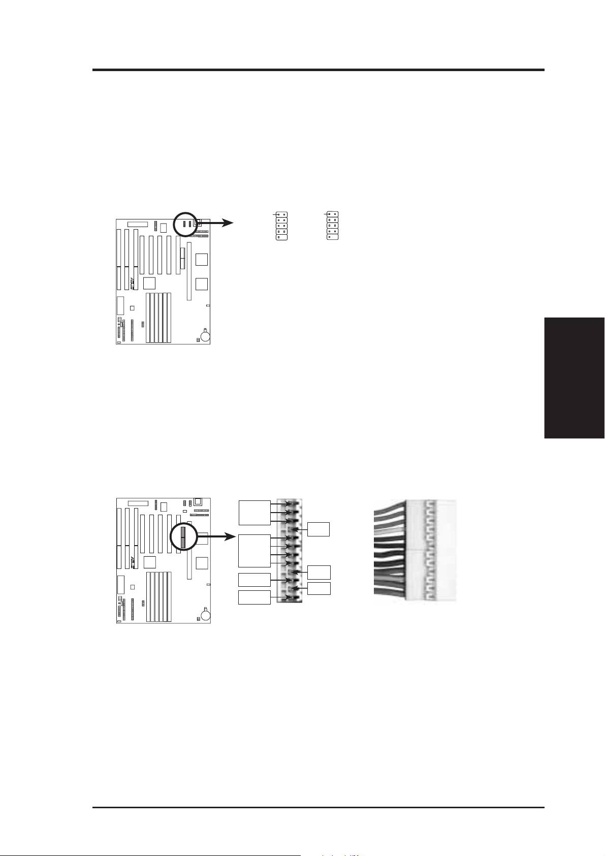
5. Serial Port Connectors (COM1, COM2)
These 10-pin block connectors support the provided serial port ribbon cables
with mounting bracket. Connect the ribbon cables to these connectors and mount
the bracket to the case on an open slot. You can make available the parallel port
and choose the IRQ through the Onboard Serial Port in Chipset Featur es of the
BIOS SOFTWARE. (Pin 10 is removed to prevent inserting in the wrong
orientation when using ribbon cables with pin 10 plugged).
Pin 1
COM 1
For these connectors to be available, you must connect
the included serial cable set from COM1 (using the 9-Pin
male) & COM2 (using the 25-Pin male) to a free expansion
R
slot opening.
TIP: You may also remove the bracket connectors and
mount them directly to the case to save expansion slot
space.
Pin 1
COM 2
Serial Port Connectors
6. AT Power Supply Connector (PWRAT)
This 12-pin block connector connects to a standard 5-volt power supply. To
connect the leads from the power supply, ensure first that the power supply is
not plugged. Most power supplies provide two plugs (P8 and P9), each containing six wires, two of which are black. Orient the connectors so that the black
wires are together.
(Connectors)
III. INSTALLATION
R
AT Power Connector
+5V
GND
+12V
PG
Power Connector
on Motherboard
-5V
-12V
+5V
RED
RED
RED
WHT
BLK
BLK
BLK
BLK
BLU
YLW
RED
ORG
Power Plugs from
Power Supply
P9
P8
Using a slight angle, align the plastic guide pins on the lead to their receptacles
on the connector. Once aligned, press the lead onto the connector until the lead
locks into place.
ASUS KN97 User’s Manual 29
Page 30
III. INSTALLATION
III. INSTALLATION
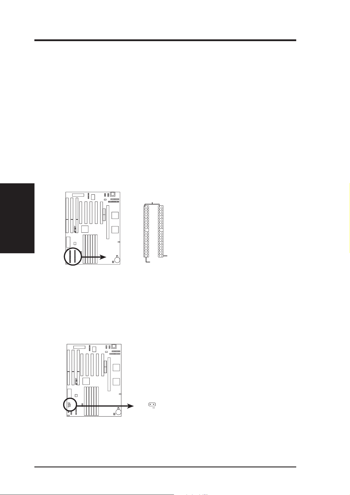
7. Primary/Secondary IDE connectors (IDE1, IDE2)
These 40-pin block connectors support the provided IDE hard disk ribbon cable.
After connecting the single end to the board, connect the two plugs at the other
end to your hard disk(s). If you install two hard disks, you must configure the
second drive to Slave mode by setting its jumper accordingly . Please refer to the
documentation of your hard disk for the jumper settings. BIOS now supports
SCSI device or IDE CD-ROM bootup (see “HDD Sequence SCSI/IDE First” &
“Boot Sequence” in the BIOS Features Setup of the BIOS SOFTWARE) (Pin
20 is removed to prevent inserting in the wrong orientation when using
ribbon cables with pin 20 plugged).
TIP: You may configure two hard disks to be both Masters using one ribbon
cable on the primary IDE connector and another ribbon cable on the secondary
IDE connector. You may install one operating system on an IDE drive and
another on a SCSI drive and select the boot disk through BIOS Features Setup.
(Connectors)
Pin 1
Orientate the IDE ribbon cable’s
red stripe to the connector’s Pin 1.
R
Primary IDE Connector
Secondary IDE Connector
IDE (Hard Drive) Connectors
8. IDE activity LED (IDELED)
This connector supplies power to the cabinet’s IDE activity LED. Read and
write activity by devices connected to the Primary or Secondary IDE connectors
will cause the LED to light up.
TIP: If the case-mounted LED
does not light, try reversing the
2-Pin plug.
R
IDE LED
+
IDE (Hard Drive) LED Lead
30 ASUS KN97 User’s Manual
Page 31
III. INSTALLATION
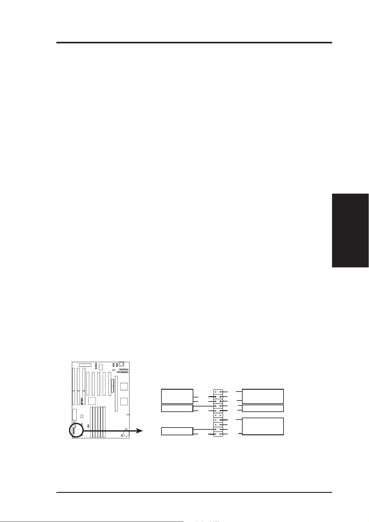
9. Turbo LED Lead (TB LEAD)
The turbo function is always on. The turbo LED connection is labeled here but
the LED will remain constantly lit while the system power is on. You may wish
to connect the Power LED from the system case to this lead.
10. SMI Suspend Switch Lead (SMI)
This allows the user to manually place the system into a suspend mode or “Green”
mode where system activity will be instantly decreased to save electricity and
expand the life of certain components when the system is not in use. This 2-pin
connector (see the figure below) connects to the case-mounted suspend switch.
If you do not have a switch for the connector, you may use the “Turbo Switch”
since it does not have a function. SMI is activated when it detects a short to
open moment and therefore leaving it shorted will not cause any problems. May
require one or two pushes depending on the position of the switch. W ake-up can
be controlled by settings in the BIOS but the keyboard will always allow wakeup (the SMI lead cannot wake-up the system). If you want to use this connector,
“Suspend Switch” in the Power Management Setup of the BIOS SOFTWARE
section should be on the default setting of Enable.
11. Reset Switch Lead (RESET)
This 2-pin connector connects to the case-mounted reset switch for rebooting
your computer without having to turn off your power switch This is a preferred
method of rebooting to prolong the life of the system’s power supply.
12. System Power LED (KEYLOCK)
This 3-pin connector connects the system power LED, which lights when the
system is powered on and blinks when it is in sleep mode.
Keyboard Lock Switch Lead (KEYLOCK)
This 2-pin connector connects to the case-mounted keyboard lock switch to allow keyboard locking.
13. Speaker Connector (SPEAKER)
This 4-pin connector connects to the case-mounted speaker.
+5V
System Power
Turbo LED
R
SMI Lead
Reset SW
+5V
GND
GND
GND
NC
GND
LOCK
GND
+5V
GND
GND
SPKR
LED
Keyboard Lock
Speaker
Connector
(Connectors)
III. INSTALLATION
System Panel Connectors
ASUS KN97 User’s Manual 31
Page 32
III. INSTALLATION
(Connectors)
III. INSTALLATION
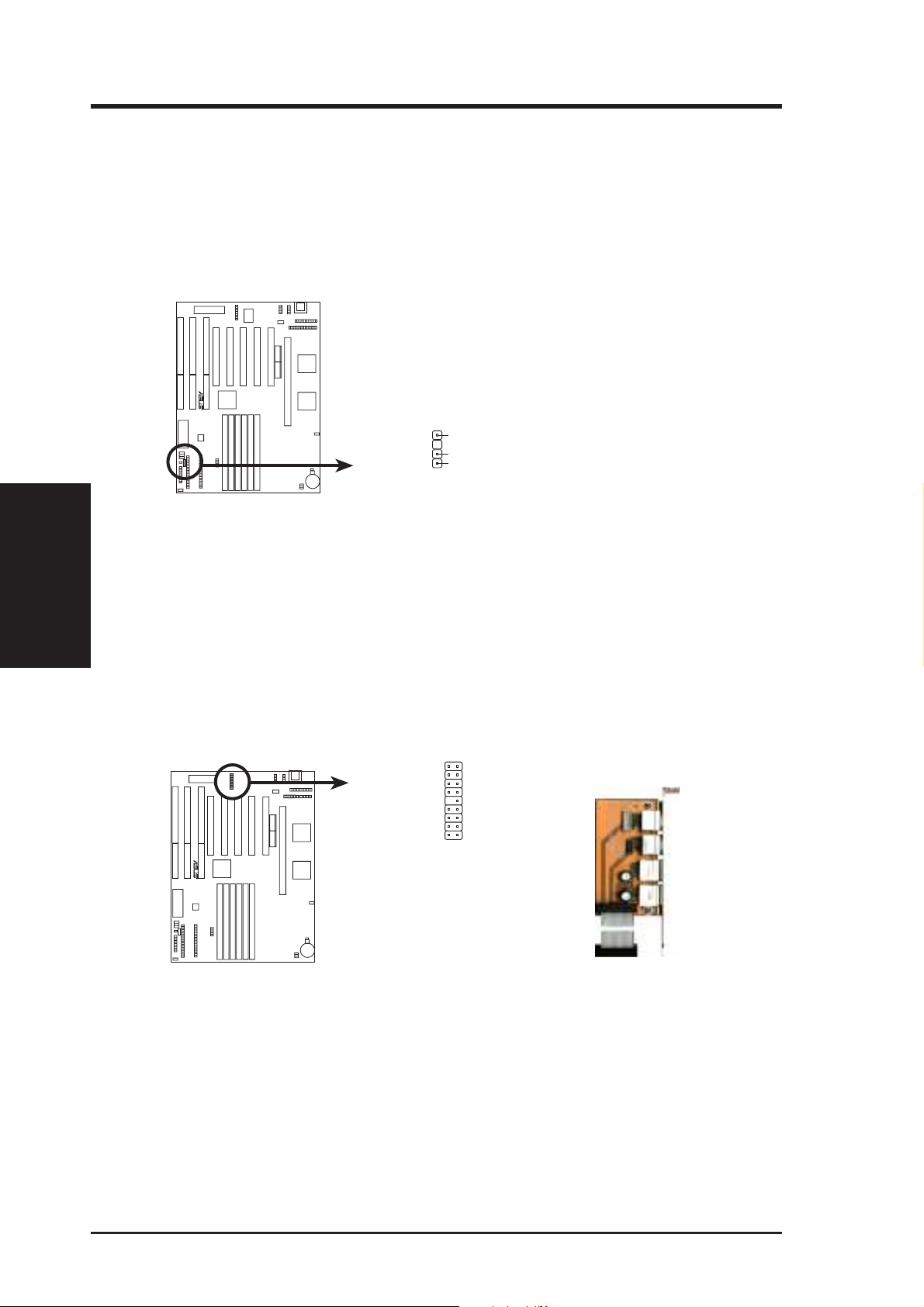
14. Chassis Open Alram Lead (CHASSIS)
This lead is for an open chassis monitor. A high level signal to the CHASSIS
lead will indicate to the system that the chassis has been opened. The +3V lead
comes from the onboard button cell battery to retain its function even if the
power cord has been unplugged from the AT power supply. Be sure that the load
on the +5V lead is minimal to prevent constant battery replacements.
R
+3 Volts (from battery)
Chassis Signal
GND
Chassis Open Alarm Lead
15. USB, Infrared (IrDA), P/2 Mouse Module Connector (USBIRMOUSE)
If you want to use USB, PS/2 mouse, or infrared devices, you need to purchase
an external connector set. The external connector set connects to the 18-pin
block and mounts to an open slot on your computer’s chassis. The system will
direct IRQ12 to the PS/2 mouse if one is detected. If not detected, expansion
cards can use IRQ12. See PS/2 Mouse Control in BIOS Features Setup and
USB Function in PnP and PCI Setup of the BIOS SOFTWARE.
10
1
9
18
10: USB +5Volt
R
11: USB Port 1 12: USB Port 1 +
13: Ground
14: (no connection)
15: PS/2 Mouse Data
16: Ground
17: IRRX
18: IRTX
USB, PS/2 Mouse, Infrared Connector
1: USB +5Volt
2: USB Port 0 3: USB Port 0 +
4: Ground
5: USB +5V
6: PS/2 Mouse Clock
7: Ground
8: FIRRX
9: IR Power +5V
USB, PS/2 Mouse,
Infrared Bracket
Infrared
PS/2 Mouse
USB 0
USB 1
Actual cable length ≈ 3in or 7.6cm
32 ASUS KN97 User’s Manual
Page 33

III. INSTALLATION
Power Connection Procedures
1. After all jumpers and connections are made, close the system case cover.
2. Make sure that all switches are off (in some systems, marked with
3. Connect the power supply cord into the power supply located on the back of
your system case as instructed by your system user’s manual.
4. Connect the power cord into a power outlet that is equipped by a surge protector .
5. You may then turn on your devices in the following order:
a. Your monitor
b. External SCSI devices (starting with the last device on the chain)
c. Your system power.
6. The power LED on the front panel of the system case will light. The monitor
LED may light up after the system’ s if it complies with “Green” standards or if
it has a power standby feature. The system will then run power-on tests. While
the tests are running, additional messages will appear on the screen. If you do
not see anything within 30 seconds from the time you turn on the power, the
system may have failed a power-on test. Recheck your jumper settings and
connections or call your retailer for assistance.
7. During power-on, hold down <Delete> to enter BIOS setup. Follow the next
section “BIOS SOFTWARE” for instructions.
).
III. INSTALLATION
(Power Connections)
* Powering Off your computer: You must first quit or shut down your operat-
ing system before switching off the power switch.
ASUS KN97 User’s Manual 33
Page 34

IV. BIOS SOFTWARE
Support Software
FILELIST.TXT – View this file to see the files included in the support software.
PFLASH.EXE – This is the Flash Memory Writer utility that updates the BIOS by
uploading a new BIOS file to the programmable flash ROM chip on the baseboard.
To determine the BIOS version, check the last four numbers of the code displayed
on the upper left corner of your screen during the test routines when you turn on
your machine.
xxxxip.xxx – BIOS file for the KN97 for use with a Pentium Pro processor on the
ASUS C-P6S1 SEC card.
xxxxi.xxx – BIOS file for the KN97 for use with a Pentium II processor.
(Flash Memory Writer)
IV. BIOS
Flash Memory Writer Utility
The flash memory writer utility must be run while the system is in real mode. In
particular, the “Update BIOS Main Block From File” and “Update BIOS Including
Boot Block and ESCD” options require real mode. To run this utility, boot from a
system floppy disk without the AUTOEXEC.BAT and CONFIG.SYS files.
ASUSTeK PNP BIOS
Copyright (C) 1995, ASUSTeK COMPUTER Inc.
Flash Type -- SST 29EE010
Current BIOS Revision: #401A0-xxxx
Choose one of the following:
1. Save Current BIOS To File
2. Update BIOS Main Block From File
3. Advanced Features
Enter Choice: [1]
Press ESC To Exit
xxxx denotes the current BIOS version stored in the Flash EPROM
FLASH MEMORY WRITER V1.5
IMPORTANT: If “unknown” is displayed after Flash Type -- , the memory chip
is not programmable or is not supported with the PnP BIOS and therefore cannot be
programmed by the Flash Memory Writer utility.
ASUS KN97 User’s Manual34
Page 35

IV. BIOS SOFTWARE
Main Menu
1. Save Current BIOS To File
This option allows you to copy the contents of the flash memory onto a floppy disk.
This gives you a backup copy of the original motherboard BIOS in case you need to
reinstall it. Create a bootable DOS diskette without AUTOEXEC.BAT and
CONFIG.SYS and save both PFLASH.EXE and the BIOS file(s) to it. Note: BIOS
FEATURES SETUP Boot Sequence needs to be set to A first in order to boot from
your disk drive A.
2. Update BIOS Main Block From File
This option updates the BIOS from a file on the disk. The file can be either a new
file or a backup file created by the “Save Current BIOS To File” option. If the boot
block in the file is different from the current boot block, this option will not update
the main block. Instead, it will display the following messages.
Boot Block of New BIOS is different from old one !!!
Please Use 'Advanced Features' to flash whole BIOS !!!
3. Advanced Features
This option displays the Advanced Features screen for clearing the PnP configuration record and updating the motherboard BIOS.
Advanced Features Menu
Advanced Features
Flash Type -- SST 29EE010
Current BIOS Revision: #401A0-xxxx
Choose one of the following:
1. Clear PNP ESCD Parameter Block
2. Update BIOS Including Boot Block and ESCD
Enter Choice: [2]
Press ESC To Exit
xxxx denotes the current BIOS version stored in the Flash EPROM
IV. BIOS
(Flash Memory Writer)
1. Clear PNP ESCD Parameter Block
This option erases the Plug-and-Play (PnP) configuration record.
2. Update BIOS Including Boot Block and ESCD
This option updates the boot block, the baseboard BIOS, and the PnP extended system configuration data (ESCD) parameter block from a new BIOS file.
ASUS KN97 User’s Manual 35
Page 36
IV. BIOS SOFTWARE
Managing & Updating your Motherboard’s BIOS
About the BIOS files:
When purchasing the ASUS KN97 motherboard, the BIOS image file (xxxxi.xxx) is
pre-programmed for the Pentium II processor . Another BIOS image file (xxxxip.xxx)
will be provided on the support disk for use with the Pentium Pro processor when
the C-P6S1 SEC card is purchased. Make sure that the correct BIOS is installed for
your motherboard and processor configuration or else your system may be unstable.
Updating BIOS (only when necessary):
1. Download an updated BIOS file from the Internet (WWW or FTP) or BBS, and save
it to the disk you created earlier . See ASUS Contact Information on page 3 for details.
2. Turn off your computer , open the system cabinet, and set the Flash ROM Boot
Block Programming jumper of the baseboard to Program or Enabled.
3. Boot from the floppy disk you created earlier.
4. At the DOS prompt, type PFLASH <Enter>
5. Select option “2. Update BIOS Main Block From File” from the Main Menu (or
option “2. Update BIOS Including Boot Block and ESCD” from the Advanced
Features menu if prompted by option 2 of the Main Menu).
(Updating BIOS)
IV. BIOS
6. On the next screen displayed, type the complete filename and extension of the new
BIOS file, and press <Enter>. The utility then updates the BIOS file from disk.
WARNING! If you encounter problems while updating the new BIOS, do not turn
off the system because doing so may prevent your system from restarting. Instead,
repeat the process. If the problem persists, use the original BIOS file you saved to
the disk earlier. If the utility is unable to successfully update a complete BIOS file,
your system may not boot up. If this happens, your system will need service.
7. After successfully updating the new BIOS file, exit the utility. Turn off the system, then set the Flash ROM Boot Block Programming jumper of the baseboard back to its default setting of Protect or Disabled.
8. Turn on your computer and hold down <Delete> to run the CMOS Setup Utility .
Select “Load Setup Defaults” to load the new BIOS, after which you may set
other items from the main menu.
ASUS KN97 User’s Manual36
Page 37
IV. BIOS SOFTWARE
6. BIOS Setup
The motherboard supports two programmable Flash ROM chips: 5 Volt and 12
Volt. Either of these memory chips can be updated when BIOS upgrades are released. Use the Flash Memory W riter utility to download the new BIOS file into the
ROM chip as described in detail in this section.
All computer motherboards provide a Setup utility program for specifying the system configuration and settings. If your motherboard came in a computer system, the
proper configuration entries may have already been made. If so, invoke the Setup
utility , as described later , and take note of the configuration settings for future refer ence; in particular, the hard disk specifications.
If you are installing the motherboard, reconfiguring your system or you receive a
Run Setup message, you will need to enter new setup information. This section
describes how to configure your system using this utility.
The BIOS ROM of the system stores the Setup utility. When you turn on the computer, the system provides you with the opportunity to run this program. This appears during the Power-On Self Test (POST). Press <Delete> to call up the Setup
utility . If you are a little bit late pressing the mentioned key(s), POST will continue
with its test routines, thus preventing you from calling up Setup. If you still need to
call Setup, reset the system by pressing <Ctrl> + <Alt> + <Delete>, or by pressing
the Reset button on the system case. You can also restart by turning the system off
and then back on again. But do so only if the first two methods fail.
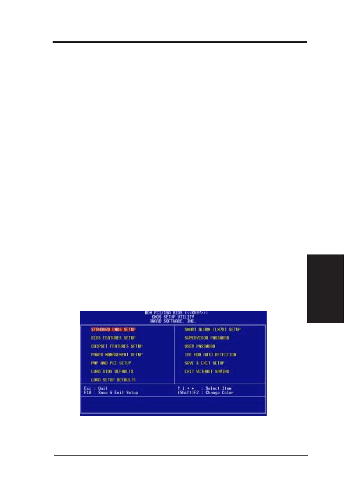
When you invoke Setup, the CMOS SETUP UTILITY main program screen will
appear with the following options:
IV. BIOS
(BIOS Setup)
ASUS KN97 User’s Manual 37
Page 38
IV. BIOS SOFTWARE
Load Defaults
The “Load BIOS Defaults” option loads the minimum settings for troubleshooting.
“Load Setup Defaults”, on the other hand, is for loading optimized defaults for
regular use. Choosing defaults at this level, will modify all applicable settings.
A section at the bottom of the above screen displays the control keys for this screen.
Take note of these keys and their respective uses. Another section just below the
control keys section displays information on the currently highlighted item in the list.
Standard CMOS Setup
This “Standard CMOS Setup” option allows you to record some basic system hardware configuration and set the system clock and error handling. If the motherboard
is already installed in a working system, you will not need to select this option
anymore. However, if the configuration stored in the CMOS memory on the board
gets lost or damaged, or if you change your system hardware configuration, you will
need to respecify the configuration values. The configuration values usually get lost
or corrupted when the power of the onboard CMOS battery weakens.
(Standard CMOS)
IV. BIOS
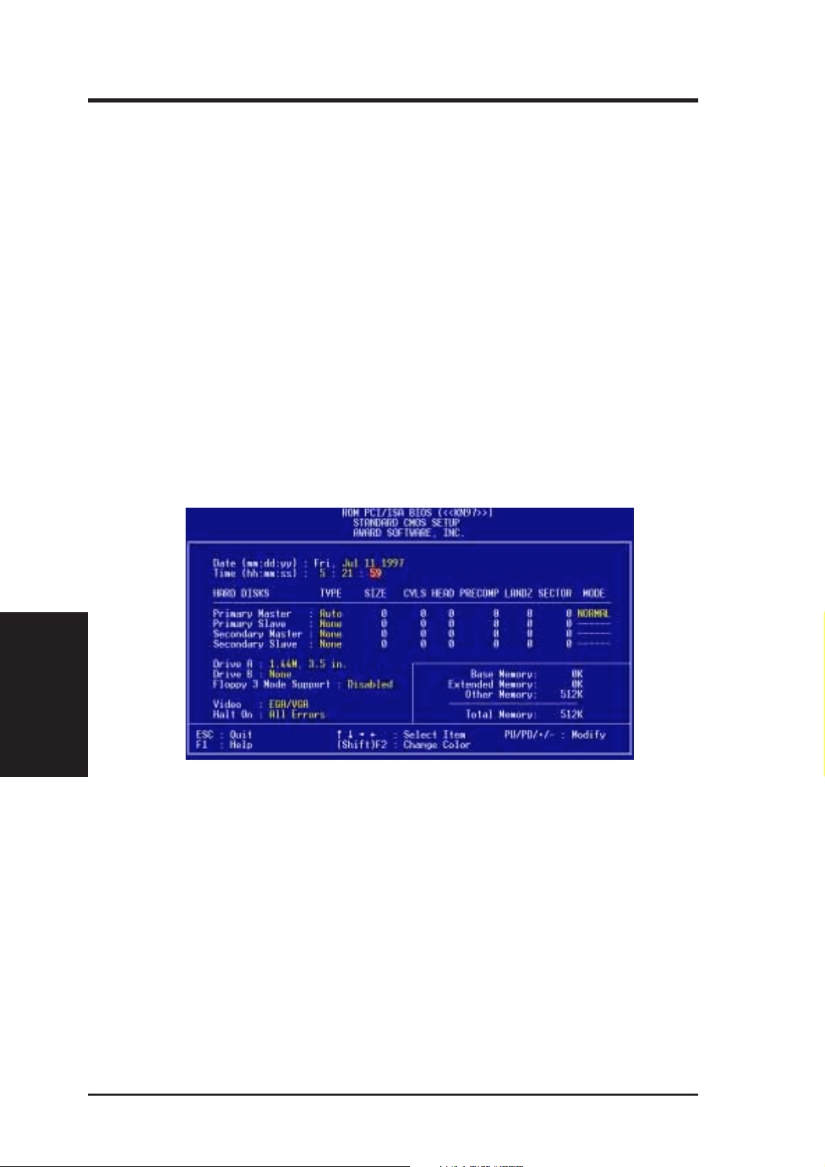
The precedong screen provides you with a list of options. At the bottom of this screen
are the control keys for this screen. Take note of these keys and their respective uses.
User-configurable fields appear in a different color. If you need information on the
selected field, press <F1>. The help menu will then appear to provide you with the
information you need. The memory display at the lower right-hand side of the screen
is read-only and automatically adjusts accordingly.
Details of Standard CMOS Setup:
Date
T o set the date, highlight the “Date” field and then press either <Page Up>/<Page Down>
or <+>/<–> to set the current date. Follow the month, day and year format. Valid values
for month, day and year are: Month: (1 to 12), Day: (1 to 31), Y ear: (up to 2079)
ASUS KN97 User’s Manual38
Page 39

IV. BIOS SOFTWARE
Time
T o set the time, highlight the “Time” field and then press either <Page Up>/<Page Down>
or <+>/<–> to set the current time. Follow the hour, minute and second format. Valid
values for hour, minute and second are: (Hour: (00 to 23), Minute: (00 to 59), Second:
(00 to 59). Press <Enter> twice if you do not want to modify the current time.
NOTE: You can bypass the date and time prompts by creating an AUT OEXEC.BA T
file. For information on how to create this file, please refer to the MS-DOS manual.
Hard Disks
This field records the specifications for all non-SCSI hard disk drives installed in
your system. The onboard PCI IDE connectors provide Primary and Secondary
channels for connecting up to four IDE hard disks or other IDE devices. Each channel can support up to two hard disks; the first of which is the “master” and the
second is the “slave”.
Specifications for SCSI hard disks need not to be entered here since they operate
using device drivers and are not supported by any the BIOS. If you install either the
optional PCI-SC200 or PCI-SC860 SCSI controller card into the motherboard, see
section VI for instructions. If you install other vendor’s SCSI controller card, refer
to their respective documentations on how to install the required SCSI drivers.
For IDE hard disk drive setup, you can:
• Use the Auto setting for detection during bootup.
• Use the IDE HDD AUTO DETECTION in the main menu to automatically
enter the drive specifications.
• Enter the specifications yourself manually by using the “User” option.
The entries for specifying the hard disk type include CYLS (number of cylinders),
HEAD (number of read/write heads), PRECOMP (write precompensation), LANDZ
(landing zone), SECTOR (number of sectors) and MODE. The SIZE field automatically adjusts according to the configuration you specify. The documentation
that comes with your hard disk should provide you with the information regarding
the drive specifications.
IV. BIOS
(Standard CMOS)
The MODE entry is for IDE hard disks only , and can be ignored for MFM and ESDI
drives. This entry provides three options: Normal, Large, LBA, or Auto (see be-
low). Set MODE to the Normal for IDE hard disk drives smaller than 528MB; set
it to LBA for drives over 528MB that support Logical Block Addressing (LBA) to
allow larger IDE hard disks; set it to Large for drives over 528MB that do not sup-
port LBA. Large type of drive can only be used with MS-DOS and is very uncommon. Most IDE drives over 528MB support the LBA mode.
ASUS KN97 User’s Manual 39
Page 40

IV. BIOS SOFTWARE
Auto detection of hard disks on bootup
For each field: Primary Master, Primary Slave, Secondary Master, and Secondary
Slave, you can select Auto under the TYPE and MODE fields. This will enable auto
detection of your IDE hard disk during bootup. This will allow you to change your
hard disks (with the power off) and then power on without having to reconfigure
your hard disk type. If you use older hard disks that do not support this feature, then
you must configure the hard disk in the standard method as described earlier by the
“User” option.
NOTE: After the IDE hard disk drive information has been entered into BIOS, new
IDE hard disk drives must be partitioned (such as with FDISK) and then formatted
before data can be read from and write on. Primary IDE hard disk drives must have
its partition set to active (also possible with FDISK).
NOTE: SETUP Defaults are noted in parenthesis next to each function heading.
Drive A / Drive B (None)
These fields record the types of floppy disk drives installed in your system. The
available options for drives A and B are: 360KB, 5.25 in.; 1.2MB, 5.25 in.; 720KB,
(Standard CMOS)
IV. BIOS
3.5 in.; 1.44MB, 3.5 in.; 2.88MB, 3.5 in.; None
To enter the configuration value for a particular drive, highlight its corresponding
field and then select the drive type using the left- or right-arrow keys.
Floppy 3 Mode Support (Disabled)
This is the Japanese standard floppy drive. The standard stores 1.2MB in a 3.5inch
diskette. This is normally disabled but you may choose from either: Drive A, Drive
B, Both, and Disabled
Video (EGA/VGA)
Set this field to the type of video display card installed in your system. The options
are EGA/VGA, CGA 49, CGA 80, and Mono (for Hercules or MDA).
If you are using a VGA or any higher resolution card, choose EGA/VGA.
Halt On (All Errors)
This field determines which types of errors will cause the system to halt. Choose from
All Errors; No Err ors; All,But Keyboard, All,But Diskette; and All,But Disk/Key.
ASUS KN97 User’s Manual40
Page 41
IV. BIOS SOFTWARE
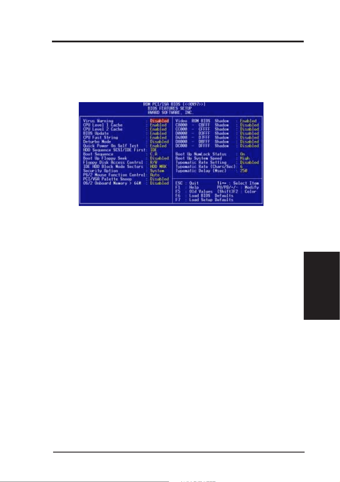
BIOS Features Setup
This “BIOS Features Setup” option consists of configuration entries that allow you
to improve your system performance, or let you set up some system features according to your preference. Some entries are required by the motherboard’s design to
remain in their default settings.
A section at the lower right of the screen displays the control keys you can use. T ake
note of these keys and their respective uses. If you need information on a particular
entry, highlight it and then press <F1>. A pop-up help menu will appear to provide
you with the information you need. <F5> loads the last set values, <F6> and <F7>
loads the BIOS default values and Setup default values, respectively.
NOTE: SETUP Defaults are noted in parenthesis next to each function heading.
Details of BIOS Features Setup
Virus Warning (Disabled)
This field protects the boot sector and partition table of your hard disk against accidental modifications. Any attempt to write to them will cause the system to halt and
display a warning message. If this occurs, you can either allow the operation to
continue or use a bootable virus-free floppy disk to reboot and investigate your
system. This setting is recommended because conflicts with new operating systems. Installation of new operating systems require that you disable this to prevent
write errors.
CPU Level 1 Cache / CPU Level 2 Cache (Enabled)
These fields allow you to choose from the default of Enabled or choose Disabled to
turn on or off the CPU’s Level 1 and Level 2 built-in cache.
IV. BIOS
(BIOS Features)
BIOS Update (Enabled)
This functions as an update loader integrated into the BIOS to supply the processor
with the required data. The BIOS will load the update on all processors during
system bootup in the default position of Enabled.
ASUS KN97 User’s Manual 41
Page 42

IV. BIOS SOFTWARE
CPU Fast String (Enabled)
Leave on default setting of Enabled for best performance.
Deturbo Mode (Disabled)
When Enabled, FLUSH# signal is held asserted to disable caching and the P6 bus
pipeline will be stalled. This allows software to run at a reduced-speed. The default
is set to Disabled to allow maximum processing speed.
Quick Power On Self Test (Enabled)
This field speeds up the Power-On Self Test (POST) routine by skipping retesting a
second, third, and forth time. Setup default setting for this field is Enabled. A
complete test of the system is done on each test.
HDD Sequence SCSI/IDE First (IDE)
When using both SCSI and IDE hard disk drives, IDE is always the boot disk using
drive letter C (default setting of IDE). This new feature allows a SCSI hard disk
drive to be the boot disk when set to SCSI. This allows multiple operating systems
to be used on both IDE and SCSI drives or the primary operating system to boot
using a SCSI hard disk drive.
Boot Sequence (C,A)
This field determines where the system looks first for an operating system. Options
are C,A; A,CDROM,C; CDROM,C,A; D,A; E,A; F,A; C only; LS/ZIP, C; and A,C.
The setup default setting is to check first the hard disk and then the floppy disk
(BIOS Features)
IV. BIOS
drive, that is, C, A.
Boot Up Floppy Seek (Disabled)
When enabled, the BIOS will seek drive A once.
Floppy Disk Access Control (R/W)
This allows protection of files from the computer system to be copied to floppy
disks by allowing the setting of Read Only to only allow reads from the floppy disk
drive but not writes. The setup default R/W allows both reads and writes.
IDE HDD Block Mode Sectors (HDD MAX)
This field enhances hard disk performance by making multi-sector transfers instead
of one sector per transfer. Most IDE drives, except older versions, can utilize this
feature. Selections are HDD MAX, Disabled, 2, 4, 8, 16, and 32.
Security Option (System)
When you specify a Supervisor Password and/or User Passwor d (explained later in
this section), the Security Option field determines when the system prompts for the
password. The default setting is System, where the system prompts for the User
Password every time you start your system. The other option is Setup, where the
system goes through its startup routine unless the Setup utility is called, when the
system prompts for the Supervisor Password.
ASUS KN97 User’s Manual42
Page 43

IV. BIOS SOFTWARE
PS/2 Mouse Function Control (Auto)
The default of Auto allows the system to detect a PS/2 mouse on bootup. If detected,
IRQ12 will be used for the PS/2 mouse. IRQ12 will be reserved for expansion cards
if a PS/2 mouse is not detected. Enabled will always reserve IRQ12, whether on
bootup a PS/2 mouse is detected or not.
PCI/VGA Palette Snoop (Disabled)
Some display cards that are nonstandard VGA such as graphics accelerators or MPEG
V ideo Cards may not show colors properly . The setting Enabled should correct this
problem. Otherwise leave this on the setup default setting of Disabled.
OS/2 Onboard Memory > 64M (Disabled)
When using OS/2 operating systems with installed DRAM of greater than 64MB,
you need to set this option to Enabled otherwise leave this on the setup default of
Disabled.
......................................................................................................................................
Video ROM BIOS Shadow (Enabled)
This field allows you to change the video BIOS location from ROM to RAM. Relocating to RAM enhances system performance, as information access is faster than
the ROM.
C8000-CBFFF to DC000-DFFFF (Disabled)
These fields are used for shadowing other expansion card ROMs. If you install
other expansion cards with ROMs on them, you will need to know which addresses
the ROMs use to shadow them specifically . Shadowing a ROM reduces the memory
available between 640K and 1024K by the amount used for this purpose.
Boot Up NumLock Status (On)
This field enables users to activate the Number Lock function upon system boot.
Boot Up System Speed (High)
This has no function and should be left on the setup default.
Typematic Rate Setting (Disabled)
When enabled, you can set the two typematic controls listed next. Setup default
setting is Disabled.
Typematic Rate (Chars/Sec) (6)
This field controls the speed at which the system registers repeated keystrokes.
Options range from 6 to 30 characters per second. Setup default setting is 6; other
settings are 8, 10, 12, 15, 20, 24, and 30.
IV. BIOS
(BIOS Features)
Typematic Delay (Msec) (250)
This field sets the time interval for displaying the first and second characters. Four
delay rate options are available: 250, 500, 750, and 1000.
ASUS KN97 User’s Manual 43
Page 44
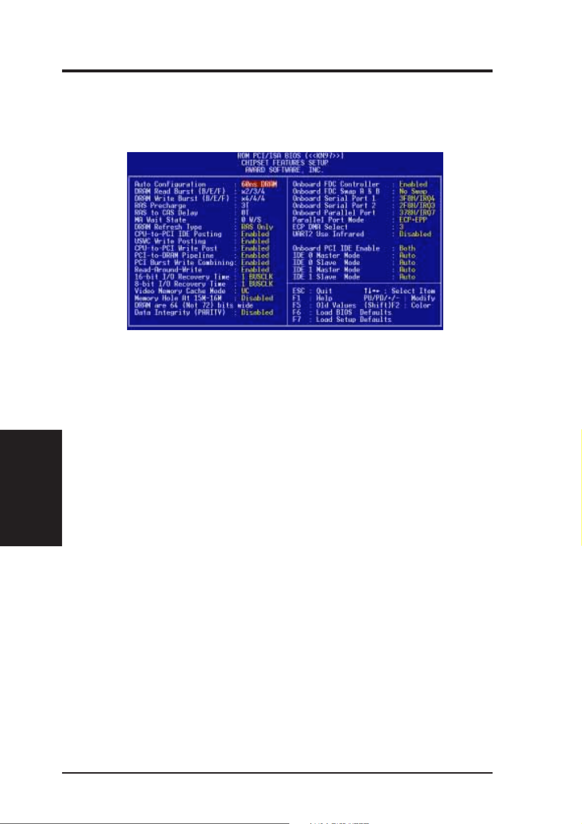
IV. BIOS SOFTWARE
Chipset Features Setup
This “Chipset Features Setup” option controls the configuration of the board’ s chipset.
Control keys for this screen are the same as for the previous screen.
NOTE: SETUP Defaults are noted in parenthesis next to each function heading.
Details of Chipset Features Setup
Auto Configuration (60ns DRAM)
The default setting of 60ns DRAM sets the optimal timings for items 2 through 6 for
(Chipset Features)
IV. BIOS
60ns DRAM modules. If you are using 70ns DRAM modules, you must change this
item to 70ns DRAM. See section III for DRAM installation information.
DRAM Refresh Type (RAS Only)
Leave on default setting of RAS Only as this is the current standard.
CPU-to-PCI IDE Posting (Enabled)
Leave on default setting of Enabled so that the CPU to PCI IDE posting cycles are
treated as normal I/O write transactions.
USWC Write Posting (Enabled)
Leave on default setting of Enabled to allow USWC write posting during
I/O bridge access.
CPU-to-PCI Write Post (Enabled)
The default setting of Enabled will increase the efficiency of the PCI bus and speed
up the execution in the processor.
PCI-to-DRAM Pipeline (Enabled)
The default of Enabled will increase the bandwidth of the path between the
PCI and the DRAM to enhance the PCI bus efficiency and DRAM accessing.
PCI Burst Write Combining (Enabled)
The default setting of Enabled will increase the efficiency of PCI bus by combining
several CPU to PCI write cycles into one. VGA performance is increased by this action.
ASUS KN97 User’s Manual44
Page 45
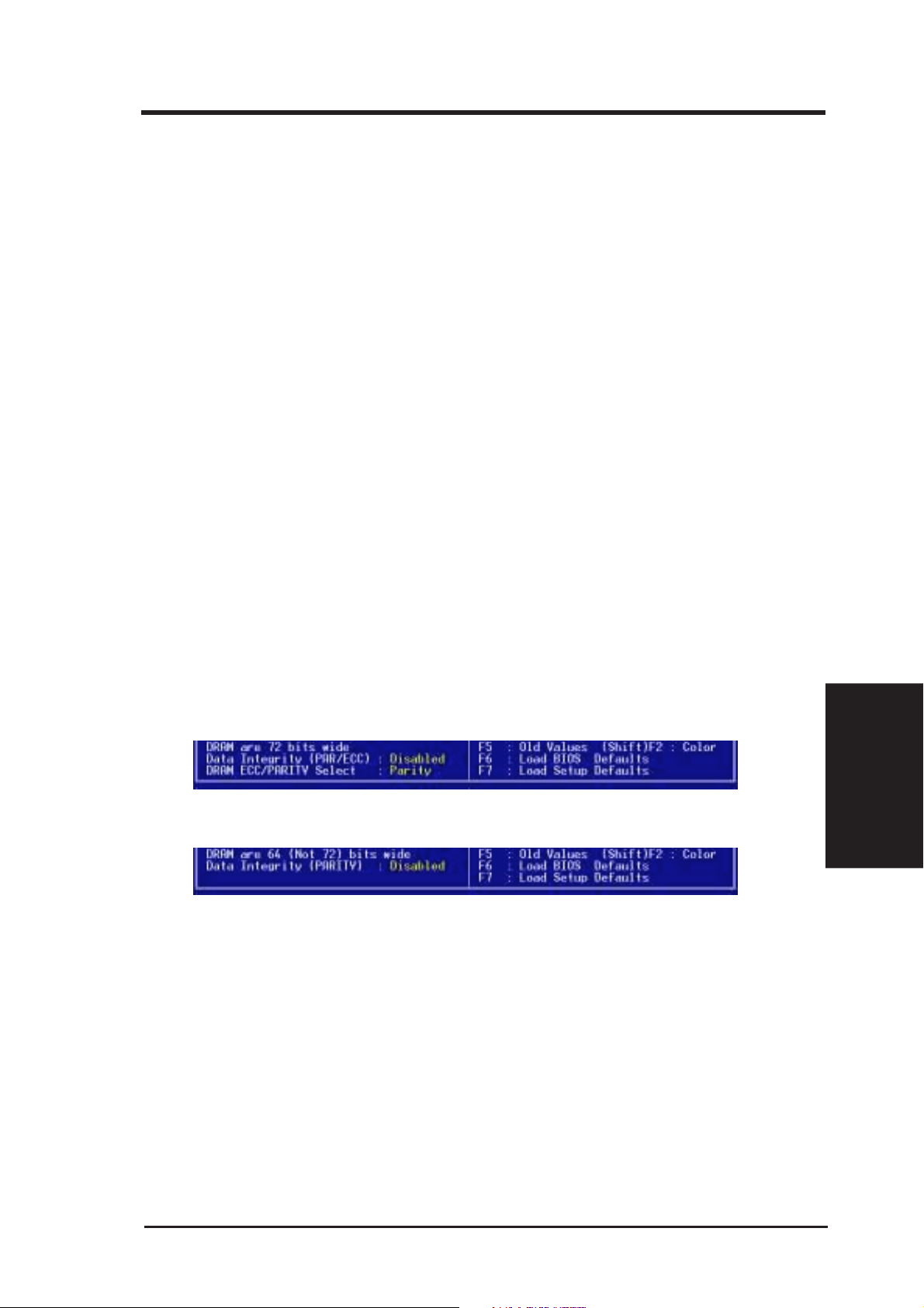
IV. BIOS SOFTWARE
Read-Around-Write (Enabled)
The default setting of Enabled will increase the execution efficiency of the processor. It allows the processor to execute read commands out of order if there is no
dependence between these read and other write commands.
16-bit I/O Recovery Time (1 BUSCLK)
Timing for 16-bit ISA cards (leave on default setting of 1 BUSCLK)
8-bit I/O Recovery Time (1 BUSCLK)
Timing for 8-bit ISA cards (leave on default setting of 1 BUSCLK)
Video Memory Cache Mode (UC)
USWC (uncacheable, speculative write combining) is a new cache technology for
the video memory of the processor. It can greatly improve the display speed by
caching the display data. You must leave this on the default setting of UC
(uncacheable) if your display card cannot support this feature or else your system
may not boot.
Memory Hole At 15M–16M (Disabled)
Enabling this feature reserves 15MB to 16MB memory address space to ISA expansion cards that specifically require this setting. This makes the memory from 15MB
and up unavailable to the system. Expansion cards can only access memory up to
16MB. The default is Disabled.
[DRAM and ECC]
If all your DRAM modules have parity chips (e.g., 8 chips + 4 parity chips), they
are considered 36bits. This motherboard sums the memory per bank and therefore
two modules will give 72bits and the following will be displayed:
If your DRAM modules do not have parity chips (e.g. 8 chips), they are considered
32bits and the following will be displayed instead:
The default of Disabled for Data Integrity will not show memory errors on your
monitor . When using parity DRAM modules, you can select ECC (Error Checking
and Correcting) to correct 1 bit memory errors that may occur in the memory , otherwise Parity is the default. (See section III for more information on DRAM memory
modules.)
....................................................................................................................................
Onboard FDC Controller (Enabled)
When Enabled (default), this field allows you to connect your floppy disk drives to
the onboard floppy disk drive connector instead of a separate controller card. If you
want to use a different controller card to connect the floppy disk drives, set this field to
Disabled.
IV. BIOS
(Chipset Features)
ASUS KN97 User’s Manual 45
Page 46

IV. BIOS SOFTWARE
Onboard FDC Swap A & B (No Swap)
This field allows you to reverse the hardware drive letter assignments of your floppy
disk drives. Two options are available: No Swap and Swap AB. If you want to switch
drive letter assignments through the onboard chipset, set this field to Swap AB.
Onboard Serial Port 1 (3F8H/IRQ4)
Settings are 3F8H/IRQ4, 2F8H/IRQ3, 3E8H/IRQ4, 2E8H/IRQ10, and Disabled for
the onboard serial connector.
Onboard Serial Port 2 (2F8H/IRQ3)
Settings are 3F8H/IRQ4, 2F8H/IRQ3, 3E8H/IRQ4, 2E8H/IRQ10, and Disabled for
the onboard serial connector.
Onboard Parallel Port (378H/IRQ7)
This field sets the address of the onboard parallel port connector. You can select
either: 3BCH / IRQ 7, 378H / IRQ 7, 278H / IRQ 5, Disabled. If you install an I/O card
with a parallel port, ensure that there is no conflict in the address assignments. The PC
can support up to three parallel ports as long as there are no conflicts for each port.
Parallel Port Mode (ECP+EPP)
This field allows you to set the operation mode of the parallel port. The setting
Normal, allows normal-speed operation but in one direction only; EPP allows bidi-
rectional parallel port operation at maximum speed; ECP allows the parallel port to
operate in bidirectional mode and at a speed faster than the maximum data transfer
rate; ECP+EPP allows normal speed operation in a two-way mode.
(Chipset Features)
IV. BIOS
ECP DMA Select (3)
This selection is available only if you select ECP or ECP+EPP in the
Parallel Port Mode. Select either DMA Channel 1, 3, or Disable.
UART2 Use Infrared (Disabled)
When enabled, this field activates the onboard infrared feature and sets the second
serial UART to support the infrared module connector on the motherboard. If your
system already has a second serial port connected to the onboard COM2 connector, it
will no longer work if you enable the infrared feature. By default, this field is set to
Disabled, which leaves the second serial port UAR T to support the COM2 serial port
connector . See IrDA-compliant infrared module connector under section III.
Onboard PCI IDE Enable (Both)
You can select to enable the primary IDE channel, secondary IDE channel, both, or
disable both channels (for systems with only SCSI drives).
IDE 0 Master/Slave Mode, IDE 1 Master/Slave Mode (Auto)
Each channel (0 and 1) has both a master and a slave making four IDE devices
possible. Because each IDE device may have a different Mode timing (0, 1, 2, 3, 4),
it is necessary for these to be independent. The default setting of Auto will allow
auto-detection to ensure optimal performance.
ASUS KN97 User’s Manual46
Page 47
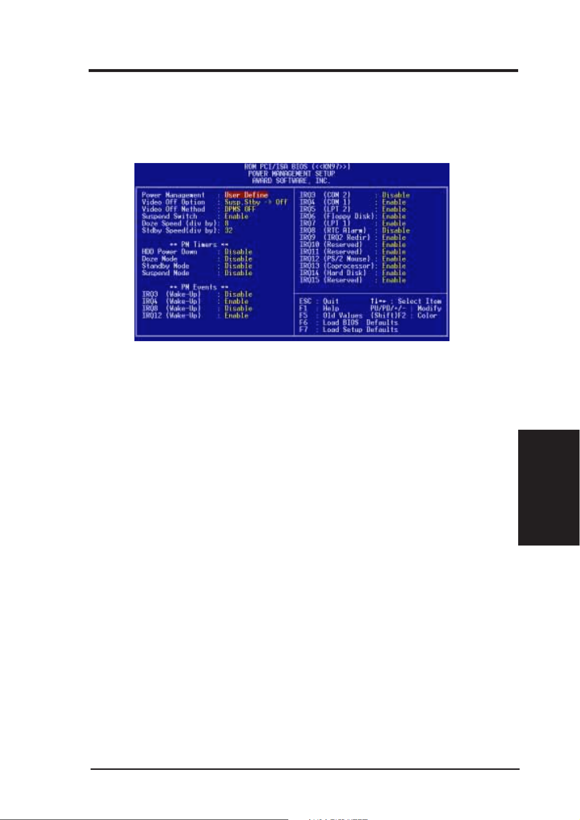
IV. BIOS SOFTWARE
Power Management Setup
This “Power Management Setup” option allows you to reduce power consumption.
This feature turns off the video display and shuts down the hard disk after a period
of inactivity.
NOTE: SETUP Defaults are noted in parenthesis next to each function heading.
Details of Power Management Setup
Power Management (User Define)
This field acts as the master control for the power management modes. Max Saving
puts the system into power saving mode after a brief period of system inactivity;
Min Saving is almost the same as Max Saving except that this time the system inactivity period is longer; Disable disables the power saving features; User Define allows you to set power saving options according to your preference.
IMPORTANT: Advanced Power Management (APM) should be installed to keep
the system time updated when the computer enters suspend mode activated by the
BIOS Power Management. For DOS environments, you need to add the statement,
DEVICE=C:\DOS\POWER.EXE, in you CONFIG.SYS. For W indows 3.x and Windows 95, you need to install Windows with the APM feature. A battery and power
cord icon labeled “Power” will appear in the “Control Panel.” Choose “Advanced”
in the Power Management Field.
Video Off Option (Susp,Stby -> Off )
This field determines when to activate the video off feature for monitor power
management. The settings are All Modes -> Off; Always On; Suspend -> Off; and
Susp,Stby -> Off .
IV. BIOS
(Power Management)
ASUS KN97 User’s Manual 47
Page 48

IV. BIOS SOFTWARE
Video Off Method (DPMS OFF)
This field defines the video off features. The following options are available: DPMS
OFF, DPMS Reduce ON, Blank Screen, V/H SYNC+Blank, DPMS Standby, and
DPMS Suspend. The DPMS (Display Power Management System) features allow
the BIOS to control the video display card if it supports the DPMS feature. Blank
Screen only blanks the screen (use this for monitors without power management or
“green” features. If set up in your system, your screen saver will not display with
Blank Screen selected). V/H SYNC+Blank blanks the screen and turns off vertical
and horizontal scanning.
Suspend Switch (Enable)
This field enables or disables the SMI connector on the motherboard. This connector connects to the lead from the Suspend switch mounted on the system case.
Doze Speed / Stdby Speed (8/32)
These two fields set the CPU speed during each mode. The number indicates what
the normal CPU speed is divided by.
PM Timers (Disable)
This section controls the time-out settings for the Power Management scheme. The
fields included in this section are “HDD Power Down”, which places the hard disk
into its lowest power consumption mode, and the Doze, Standby and Suspend system inactivation modes.
The system automatically “wakes up” from any power saving mode when there is
system activity such as when a key is pressed from the keyboard, or when there is
activity detected from the enabled IRQ channels.
(Power Management)
HDD Power Down shuts down any IDE hard disk drives in the system after a pe-
IV. BIOS
riod of inactivity. This time period is user-configurable to 1–15 Min or Disable.
This feature does not affect SCSI hard drives.
The Doze Mode, Standby Mode, and Suspend Mode fields set the period of time
after which each of these modes activate: 1 Min, 2 Min, 4 Min, 8 Min, 10 Min, 20
Min, 30 Min, 1 Hour, 2 Hour, and 4 Hour.
PM Events
This section sets the wake-up call of the system. If activity is detected from any enabled
IRQ channels in the left-hand group, the system wakes up from suspended mode. You
can enable power management for IRQ3–IRQ15 individually in the list at the right of
the screen. The power management feature will work on the enabled IRQ channels.
NOTE: A Microsoft serial mouse or compatible will use either COM1 (IRQ4) or
COM2 (IRQ3), and a PS/2 mouse will use IRQ12. If you know which IRQ your
mouse is using, you can enable the wake-up Event for that IRQ here and the system
will wake up when you move the mouse or click its button.
.......................................................................................................................................
IRQ3 (device)-IRQ15 (device)
You can individually Enable or Disable each IRQ to include in the sleep function.
IRQ8 (RTC Alarm) is usually set to Disable so that any software alarm clock or
event calendar can wake up the system.
ASUS KN97 User’s Manual48
Page 49
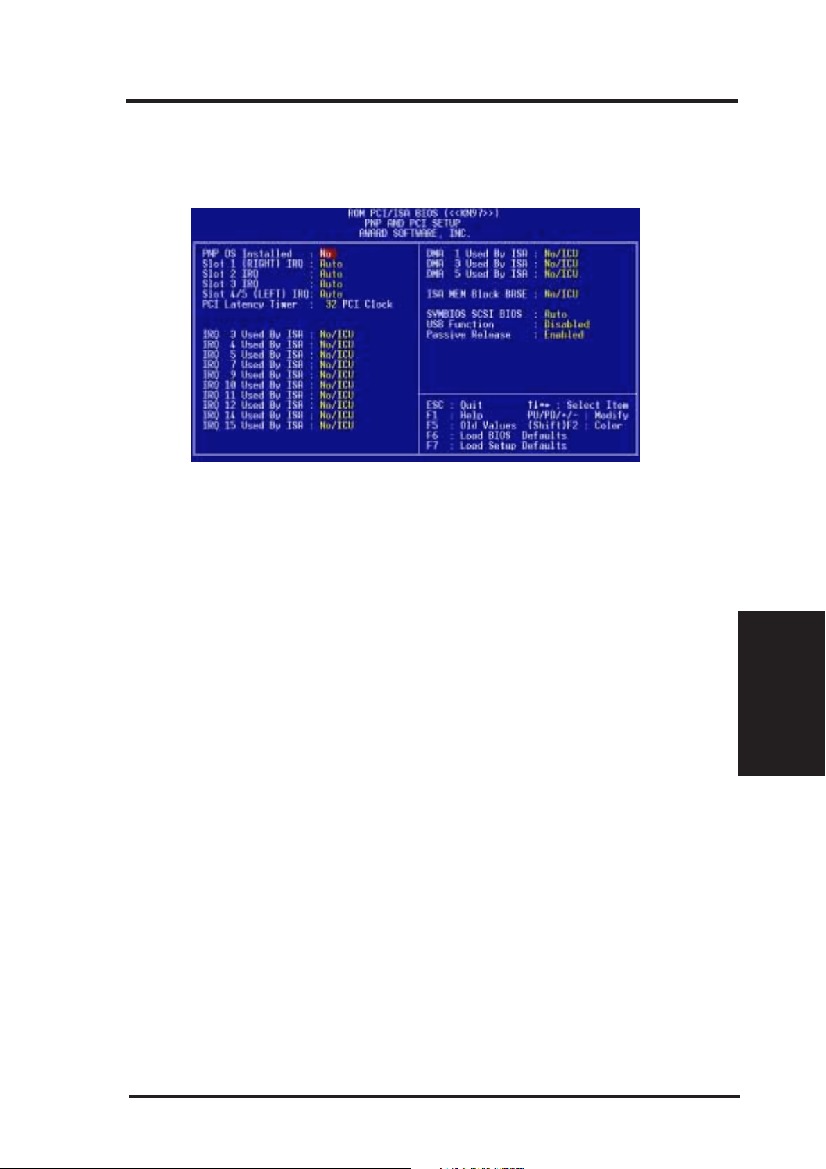
IV. BIOS SOFTWARE
PNP and PCI Setup
This “PNP and PCI Setup” option configures the PCI bus slots. All PCI bus slots on
the system use INTA#, thus all installed PCI cards must be set to this value.
NOTE: SETUP Defaults are noted in parenthesis next to each function heading.
Details of PNP and PCI Setup
PNP OS Installed (No)
This field allows you to use a Plug-and-Play (PnP) operating system to configure
the PCI bus slots instead of using the BIOS. Thus interrupts may be reassigned by
the OS when Yes is selected. When a non-PnP OS is installed or to prevent reassigning of interrupt settings, select the default setting of No.
Slot 1 (RIGHT) IRQ to Slot 4/5 (LEFT) IRQ (Auto)
These fields set how IRQ use is determined for each PCI slot. The default setting for
each field is Auto, which uses auto-routing to determine IRQ use. The other options are
manual settings of NA, 5, 7, 9, 10, 11, 12, 14 or 15 for each slot.
PCI Latency Timer (32 PCI Clock)
The default setting of 32 PCI Clock enables maximum PCI performance for this
motherboard.
IRQ xx Used By ISA (No/ICU)
These fields indicate whether or not the displayed IRQ for each field is being used
by a legacy (non-PnP) ISA card. Two options are available: No/ICU and Yes. The
first option, the default value, indicates either that the displayed IRQ is not used or
an ISA Configuration Utility (ICU) is being used to determine if an ISA card is
using that IRQ. If you install a legacy ISA card that requires a unique IRQ, and you
are not using an ICU, you must set the field for that IRQ to Yes. For example: If you
install a legacy ISA card that requires IRQ 10, then set IRQ10 Used By ISA to Yes.
......................................................................................................................................
IV. BIOS
(Plug & Play / PCI)
ASUS KN97 User’s Manual 49
Page 50

IV. BIOS SOFTWARE
DMA x Used By ISA (No/ICU)
These fields indicate whether or not the displayed DMA channel for each field is
being used by a legacy (non-PnP) ISA card. Available options include: No/ICU and
Yes. The first option, the default setting, indicates either that the displayed DMA
channel is not used or an ICU is being used to determine if an ISA card is using that
channel. If you install a legacy ISA card that requires a unique DMA channel, and
you are not using an ICU, you must set the field for that channel to Yes.
ISA MEM Block BASE (No/ICU)
This field allows you to set the base address and block size of a legacy ISA card that
uses any memory segment within the C800H and DFFFH address range. If you
have such a card, and you are not using an ICU to specify its address range, select a
base address from the six available options; the ISA MEM Block SIZE field will
then appear for selecting the block size. If you have more than one legacy ISA card
in your system that requires to use this address range, you can increase the block
size to either 8K, 16K, 36K, or 64K. If you are using an ICU to accomplish this task,
leave ISA MEM Block BASE to its default setting of No/ICU.
SYMBIOS SCSI BIOS (Auto)
The default uses Auto settings for the onboard SCSI BIOS. If you do not want to use
the onboard SCSI BIOS, choose Disabled
USB Function (Disabled)
(Plug & Play / PCI)
IV. BIOS
This motherboard supports Universal Serial Bus (USB) devices but current operating systems do not. The default is set to Disabled until support disks and USB
devices are available in which time you can set this function to Enabled.
Passive Release (Enabled)
This function allows the passive release to be Enabled or Disabled. The default
setting of Enabled allows better performance.
ASUS KN97 User’s Manual50
Page 51
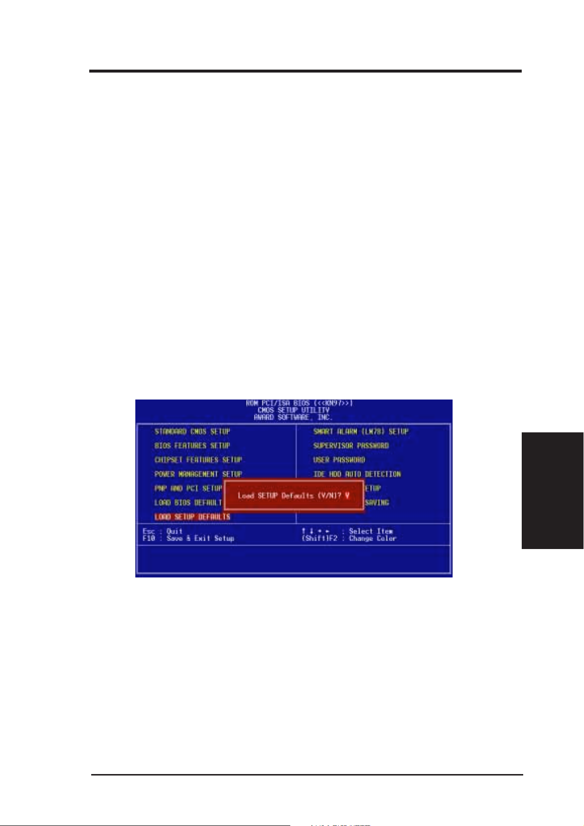
IV. BIOS SOFTWARE
Load BIOS Defaults
This “Load BIOS Defaults” option allows you to load the troubleshooting default
values permanently stored in the BIOS ROM. These default settings are non-optimal and disable all high performance features. To load these default settings, highlight “Load BIOS Defaults” on the main screen and then press <Enter>. The system
displays a confirmation message on the screen. Press <Y> and then <Enter> to
confirm. Press <N> and then <Enter> to abort. This feature does not affect the
fields on the Standard CMOS Setup screen.
Load Setup Defaults
This “Load Setup Defaults” option allows you to load the default values to the system configuration fields. These default values are the optimized configuration settings for the system. To load these default values, highlight “Load Setup Defaults”
on the main screen and then press <Enter>. The system displays a confirmation
message on the screen. Press <Y> and then <Enter> to confirm. Press <N> and
then <Enter> to abort. This feature does not affect the fields on the Standard CMOS
Setup screen.
ASUS KN97 User’s Manual 51
IV. BIOS
(Load Defaults)
Page 52
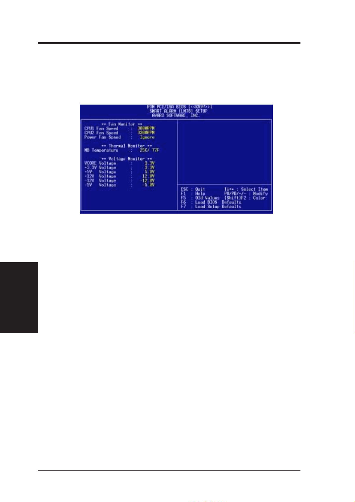
IV. BIOS SOFTWARE
Smart Alarm (LM78) Setup
This menu controls the functions of the LM78 hardware monitor chip on this motherboard. Certain hardware components are necessary for the all the features to be
available.
NOTE: SETUP Defaults are noted in parenthesis next to each function heading.
Details of Smart Alarm (LM78) Setup
(Hardware Monitor)
IV. BIOS
Fan Monitor: CPU1 Fan Speed, CPU2 Fan Speed, Power Fan Speed (xxxxRPM)
The onboard hardware monitor is able to detect the Chassis Fan Speed, CPU Fan
Speed, and the Power Supply Fan Speed in Rotations Per Minute (RPM). These
values refresh upon any key entry in the BIOS setup screens. Set to Ignore if one of
these are not used so that error messages will not be given.
Thermal Monitor: MB Temperature (xxxC/xxxF)
The onboard hardware monitor is able to detect the Motherboard temperatures. These
values refresh upon key entries. Set to Ignore only if necessary.
Voltage Monitor: VCORE, +3.3V, +5V, +12V, -12V, -5V (+/- xx.xV)
The onboard hardware monitor is able to detect the voltages put out by the voltage
regulators. These values refresh upon key entries. Set to Ignore only if necessary.
NOTE: If any of the monitored items are out of range during system bootup, you
will be prompted by this message: “Hardware Monitor found an error, enter POWER
MANAGEMENT SETUP for details.” The bottom of the screen will instruct you
to: “Press F1 to continue, DEL to enter SETUP.”
ASUS KN97 User’s Manual52
Page 53
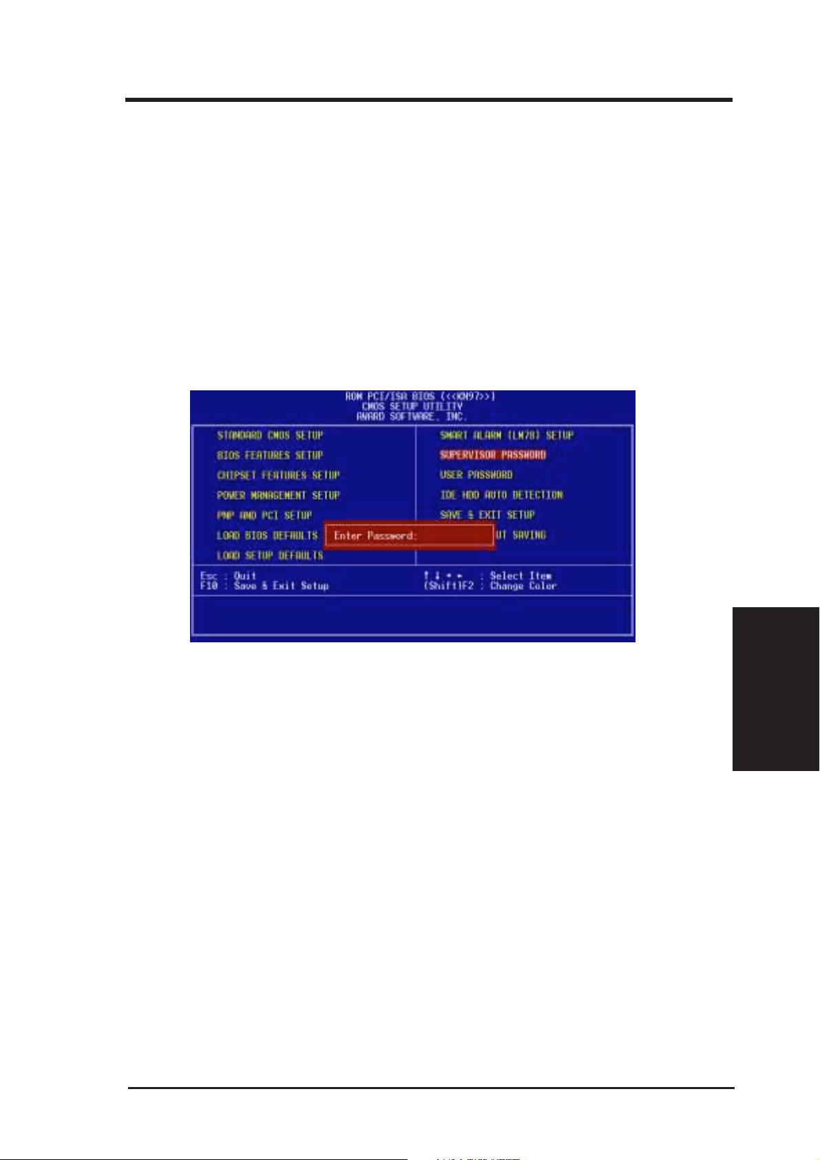
IV. BIOS SOFTWARE
Supervisor Password and User Password
These two options set the system passwords. “Supervisor Password” sets a password that will be used to protect the system and the Setup utility; “User Password”
sets a password that will be used exclusively on the system. By default, the system
comes without any passwords. To specify a password, highlight the type you want
and then press <Enter>. A password prompt appears on the screen. Taking note that
the password is case sensitive, and can be up to 8 alphanumeric characters long, type
in your password and then press <Enter>. The system confirms your password by
asking you to type it again. After setting a password, the screen automatically reverts to the main screen.
To implement password protection, specify in the “Security Option” field of the
BIOS Features Setup screen when the system will prompt for the password. If you
want to disable either password, press <Enter> instead of entering a new password
when the “Enter Password” prompt appears. A message confirms the password has
been disabled.
NOTE: If you forget the password, see CMOS RAM in section III for procedures
on clearing the CMOS.
IV. BIOS
(Passwords)
ASUS KN97 User’s Manual 53
Page 54
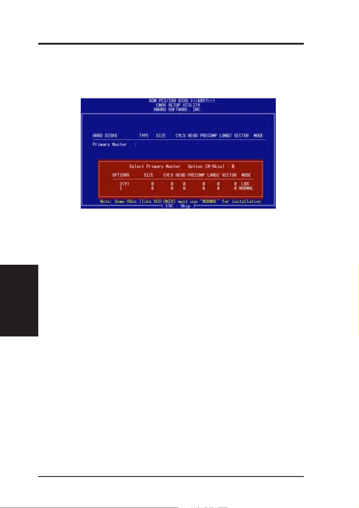
IV. BIOS SOFTWARE
IDE HDD Auto Detection
This “IDE HDD Auto Detection” option detects the parameters of an IDE hard disk
drive, and automatically enters them into the Standard CMOS Setup screen.
Up to four IDE drives can be detected, with parameters for each listed inside the
box. To accept the optimal entries, press <Y> or else select from the numbers displayed under the OPTIONS field (2, 1, 3 in this case); to skip to the next drive, press
<N>. If you accept the values, the parameters will appear listed beside the drive
(Hard Disk Detect)
IV. BIOS
letter on the screen. The process then proceeds to the next drive letter. Pressing
<N> to skip rather than to accept a set of parameters causes the program to enter
zeros after that drive letter.
Remember that if you are using another IDE controller that does not feature Enhanced IDE support for four devices, you can only install two IDE hard disk drives.
Y our IDE controller must support the Enhanced IDE features in order to use Drive E
and Drive F. The onboard PCI IDE controller supports Enhanced IDE, with two
connectors for connecting up to four IDE devices. If you want to use another controller that supports four drives, you must disable the onboard IDE controller in the
Chipset Features Setup screen.
When auto-detection is completed, the program automatically enters all entries you
accepted on the field for that drive in the Standard CMOS Setup screen. Skipped
entries are ignored and are not entered in the screen.
If you are auto-detecting a hard disk that supports the LBA mode, three lines will
appear in the parameter box. Choose the line that lists LBA for an LBA drive. Do
not select Large or Normal.
The auto-detection feature can only detect one set of parameters for a particular IDE
hard drive. Some IDE drives can use more than one set. This is not a problem if the
drive is new and empty.
ASUS KN97 User’s Manual54
Page 55
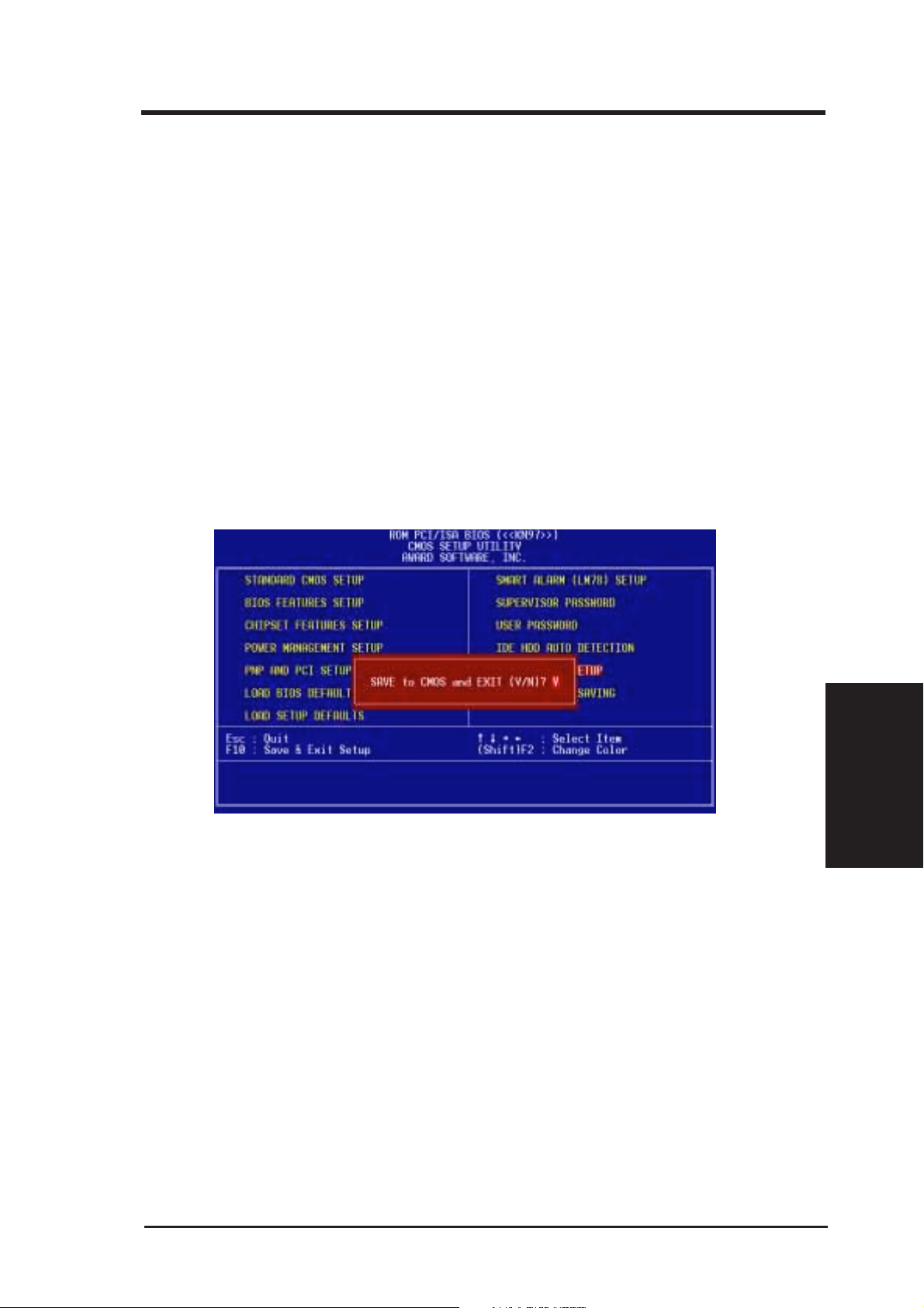
IV. BIOS SOFTWARE
IMPORTANT: If your hard disk was already formatted on an older previous system,
incorrect parameters may be detected. You will need to enter the correct parameters
manually or use low-level format if you do not need the data stored on the hard disk.
If the parameters listed differ from the ones used when the disk was formatted, the
disk will not be readable. If the auto-detected parameters do not match the ones that
should be used for your disk, do not accept them. Press <N> to reject the presented
settings and enter the correct ones manually from the Standard CMOS Setup screen.
Save & Exit Setup
Select this option to save into the CMOS memory all modifications you specified
during the current session. To save the configuration changes, highlight the “Save
& Exit Setup” option on the main screen, type “Y”, and then press <Enter>.
Exit Without Saving
Select this option to exit the Setup utility without saving the modifications you specify
during the current session. To exit without saving, highlight the “Exit Without Saving” option on the main screen and then press <Enter>.
ASUS KN97 User’s Manual 55
IV. BIOS
(Save & Exit)
Page 56

V. DESKTOP MANAGEMENT
Desktop Management Interface (DMI)
Introducing the ASUS DMI Configuration Utility
This motherboard supports DMI within the BIOS level and provides a DMI Configuration Utility to maintain the Management Information Format Database (MIFD).
DMI is able to auto-detect and record information pertinent to a computer’s system
such as the CPU type, CPU speed, and internal/external frequencies, and memory
size. The onboard BIOS will detect as many system information as possible and
store those collected information in a 4KB block in the motherboard’ s Flash EPROM
and allow the DMI to retrieve data from this database. Unlike other BIOS software,
the BIOS on this motherboard uses the same technology implemented for Plug and
Play to allow dynamic real-time updating of DMI information versus creating a new
BIOS image file and requiring the user to update the whole BIOS. This DMI Configuration Utility also allows the system integrator or end user to add additional
information into the MIFD such as serial numbers, housing configurations, and vendor information. Those information not detected by the motherboard BIOS and has
to be manually entered through the DMI Configuration Utility and updated into the
MIFD. This DMI Configuration Utility provides the same reliability as PnP updating and will prevent the refreshing failures associated with updating the entire BIOS.
System Requirements
The DMI Configuration Utility (DMICFG.EXE) must be used in real mode in order
for the program to run, the base memory must be at least 180K. Memory managers
like HIMEM.SYS (required by windows) must not be installed. You can boot up
from a system diskette without AUTOEXEC.BAT and CONFIG.SYS files, “REM”
HIMEM.SYS in the CONFIG.SYS, or press <F5> during bootup to bypass your
AUTOEXEC.BAT and CONFIG.SYS files.
(DMI Introduction)
V. DMI
ASUS KN97 User’s Manual56
Page 57
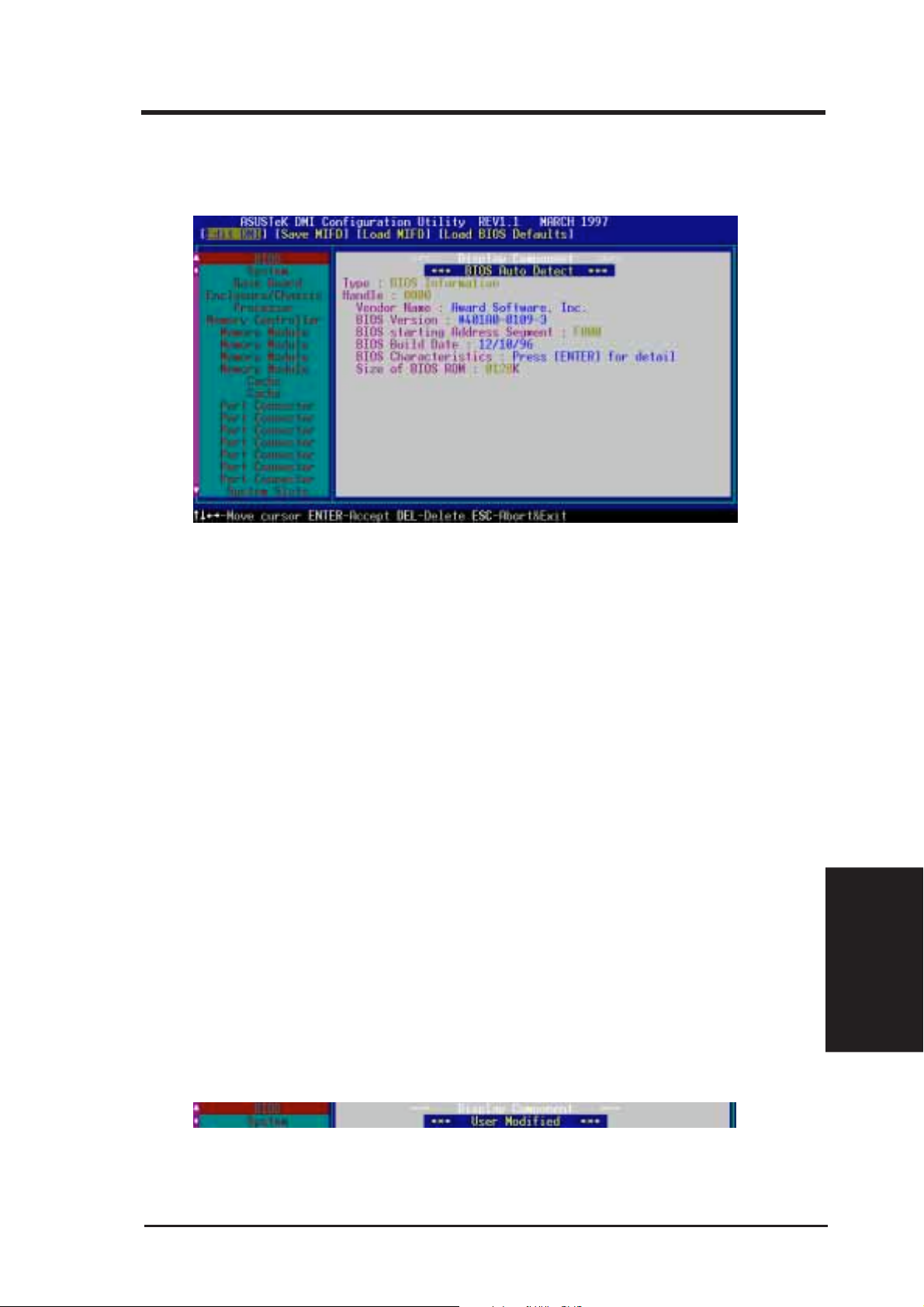
V. DESKTOP MANAGEMENT
Using the ASUS DMI Configuration Utility
Edit DMI (or delete)
Use the ←→ (left-right) cursors to move the top menu items and the ↑↓ (up-down)
cursor to move between the left hand menu items. The bottom of the screen will
show the available keys for each screen. Press enter at the menu item to enter the
right hand screen for editing. “Edit component” appears on top. The reversed color
field is the current cursor position and the blue text are available for editing. The
orange text shows auto-detected information and are not available for editing. The
blue text “Press [ENTER] for detail” contains a second pop-up menu is available,
use the + - (plus-minus) keys to change the settings. Enter to exit and save, ESC to
exit and not save.
If the user has made changes, ESC will prompt you to answer Y or N. Enter Y to go
back to the left-hand screen and save, enter N to go back to left-hand screen and not
save. If editing has not been made, ESC will send you back to the left hand menu
without any messages.
Notes
A heading, *** BIOS Auto Detect *** appears on the right for each menu item
on the left side that has been auto detected by the system BIOS.
A heading,
been modified by the user.
*** User Modified *** will appear on the right for menu items that has
V. DMI
(Using DMI Utility)
ASUS KN97 User’s Manual 57
Page 58
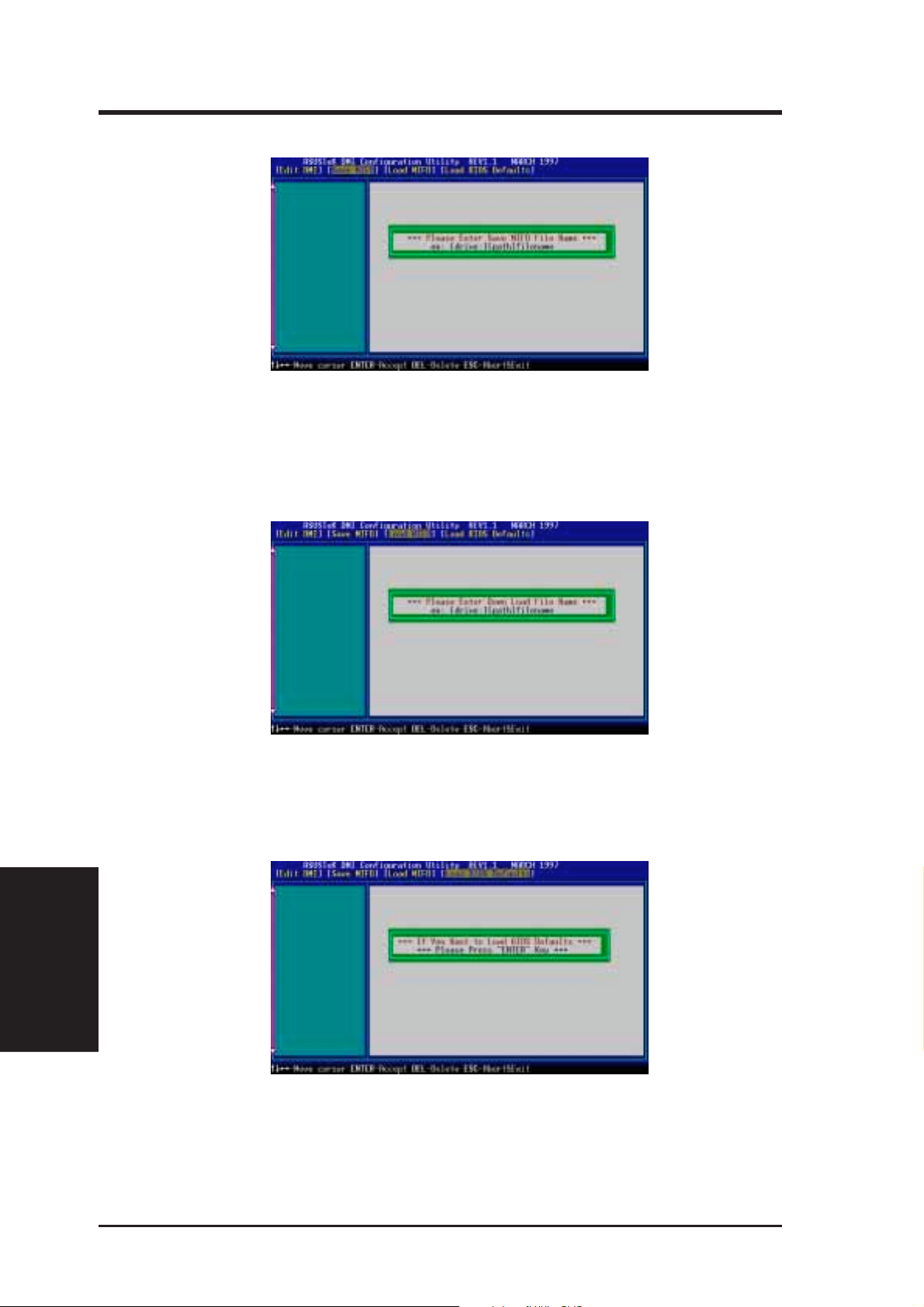
V. DESKTOP MANAGEMENT
Save MIFD
Y ou can save the MIFD (normally only saved to flash ROM) to a file by entering the
drive and path here. If you want to cancel save, you may press ESC and a message
“Bad File Name” appears here to show it was not saved.
Load MIFD
You can load the disk file to memory by entering a drive and path and file name
here.
Load BIOS Defaults
(Using DMI Utility)
V. DMI
You can load the BIOS defaults from a MIFD file and can clear all user modified
and added data. You must reboot your computer in order for the defaults to be saved
back into the Flash BIOS.
ASUS KN97 User’s Manual58
Page 59
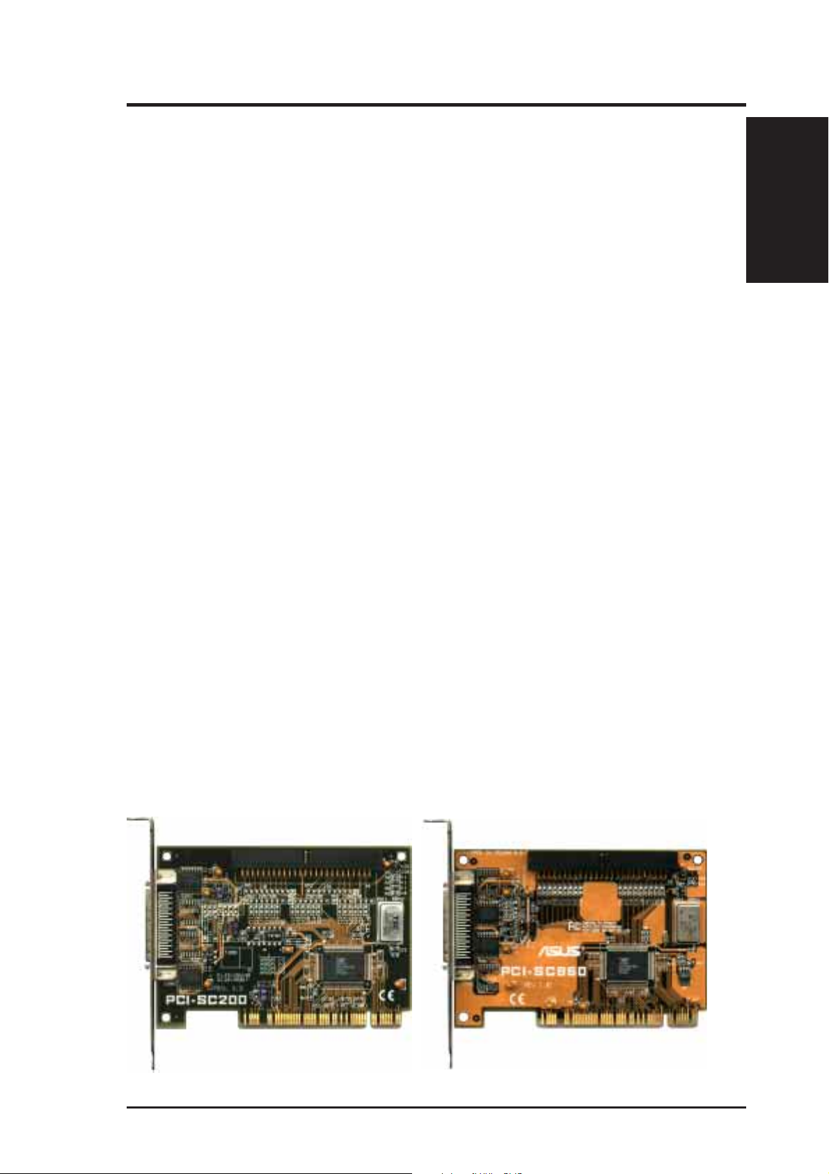
VI. ASUS PCI SCSI Cards
Symbios SCSI BIOS and Drivers
Aside from the system BIOS, the Flash memory chip on the motherboard also contains the Symbios SCSI BIOS. This Symbios SCSI BIOS works in conjunction with
the optional ASUS PCI-SC200 controller card to provide Fast SCSI-2 interface when
using compatible SCSI devices or the ASUS PCI-SC860 SCSI controller cards to
provide Ultra-Fast SCSI-2 interface when using Ultra-Fast SCSI-2 devices.
All SCSI devices you install on your system require driver software to function.
The Symbios SCSI BIOS directly supports SCSI hard disks under the DOS, Windows and OS/2 environments. It also uses device drivers from the DOS floppy disk
included in the ASUS PCI-SC200 and ASUS PCI-SC860 controller card packages
to support hard disks and other SCSI devices working under DOS, Microsoft Windows, Microsoft W indows NT, Novell NetWare and IBM OS/2. These drivers provide higher performance than the direct BIOS support. To use these drivers, you
must install them into your system and add them to your system configuration files.
Driver support for SCSI devices used with SCO UNIX is also provided. These
drivers are included in the second SCO UNIX floppy disk. Windows 95 support is
also available using the device drivers included within the Windows software. The
ASUS PCI-SC200 and ASUS PCI-SC860 are Plug and Play adapters that are auto
detected by BIOS and current operating systems that support Plug and Play features.
(SCSI BIOS)
VI. ASUS SCSI Cards
For information about these drivers and their usage, please view the Readme files
included in the driver packages.
ASUS PCI-SC200 & PCI-SC860 SCSI Cards
The ASUS PCI-SC200 or the ASUS PCI-SC860 may be bundled with your mother board or purchased separately . Both cards provide the option of connecting internal
or external SCSI devices for a total of 7 devices on each SCSI card.
ASUS KN97 User’s Manual 59
Page 60
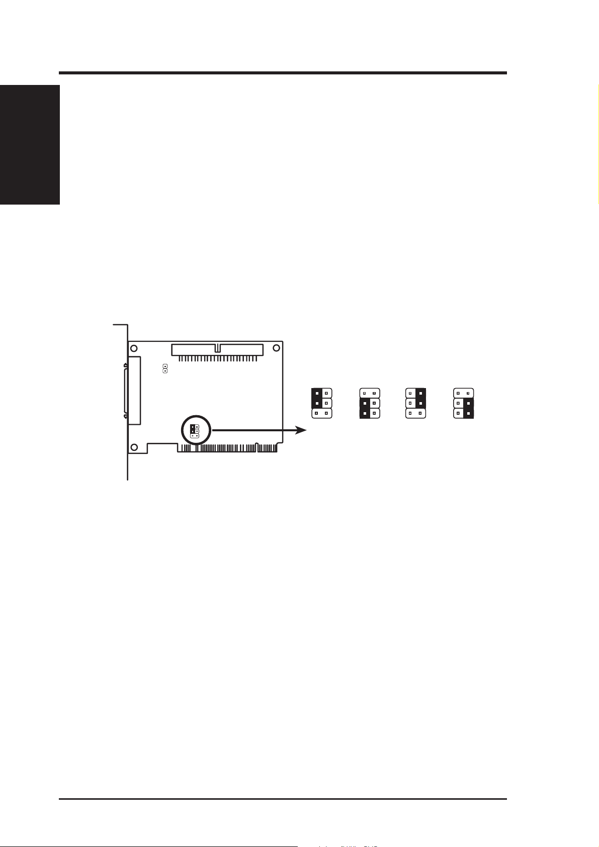
VI. ASUS SCSI Cards
Setting Up the ASUS PCI-SC200 & PCI-SC860
VI. ASUS PCI SCSI Cards
(Setup)
There are two jumper settings you may need to make on the ASUS PCI-SC200 to set
it up. One setting assigns the PCI INT interrupt, the other sets the card’ s termination.
The ASUS PCI-SC860 has no jumper settings but you should read the “Terminator
Requirements.”
Setting the INT Assignment for the ASUS PCI-SC200
You must use PCI INT A setting in order to properly assign the ASUS PCI-SC200's
interrupt. On the ASUS PCI-SC200, you assign the INT by setting jumper JP1 or
JP2. The default setting for the card already is INT A, so you do not need to change
the setting to use the ASUS PCI-SC200 with this motherboard.
JP 1JP
2
INT A (Def)
JP 1JP
2
1
2
3
INT B
JP 1JP
2
1
2
3
INT C
JP 1JP
1
2
3
2
1
2
3
INT D
Interrupt Settings (A, B, C, or D)
Terminator Requirements for SCSI Devices
SCSI devices are connected together in a “chain” by cables. Internal devices connect to the ASUS PCI-SC200 or ASUS PCI-SC860 with a fifty-pin flat ribbon cable.
External devices connect to the external port with a SCSI-2 cable. If there are more
than one internal or external devices, additional devices are connected with cables
to form a “daisy chain.” T erminating the devices on the ends of the SCSI Bus “chain”
is necessary for SCSI devices to work properly . Termination of the devices between
the ends must be Disabled.
60 ASUS KN97 User’s Manual
Page 61
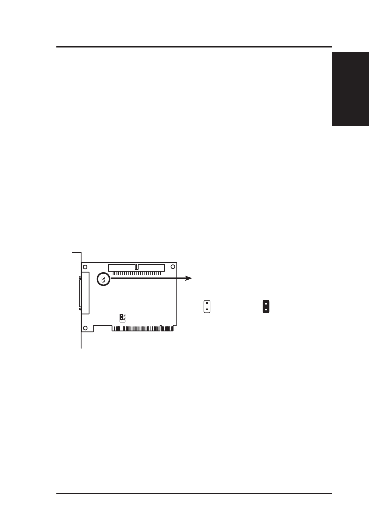
VI. ASUS PCI SCSI Cards
Terminator Settings for the ASUS PCI-SC860
Many SCSI devices including the ASUS PCI-SC860 use a set of onboard active
resistors to terminate the devices at the ends automatically. Automatic termination
requires that the SCSI devices be connected in a straight linear connection or “chain.”
Connect SCSI devices to one or two of the SCSI connectors in a linear “chain” for
auto termination of the ASUS PCI-SC860 to be effective. Other formations will
cause your SCSI devices to not mount properly . You must use the end of the ribbon
cable when using the internal connector(s) to keep a linear path.
Additional Note: The Symbios Logic SCSI Configuration Utility is a powerful
tool. If, while using it, you somehow disable all your controllers or cannot enter
the configuration utility, pressing “Ctrl-A” after memory count during r eboot
allows you to recover and reconfigure.
Terminator Settings for the ASUS PCI-SC200
The ASUS PCI-SC200, on the other hand, has “active” termination that you must
set using jumper JP5. There are two settings, "terminated" and "not terminated," as
shown below.
(Jumpers)
VI. ASUS SCSI Cards
JP
5
Terminated (Default) Not Terminated
Terminator Setting (Terminated / Not Terminated)
JP
5
Decide whether or not you need to terminate the ASUS PCI-SC200 based on its
position in the SCSI chain. Only the devices at each end of the chain need to be
terminated. If you have only internal or only external devices connected to the
ASUS PCI-SC200, then you must terminate the ASUS PCI-SC200. If you have
both internal and external devices connected, you must not terminate the card. See
the following example which illustrates this concept.
ASUS KN97 User’s Manual 61
Page 62
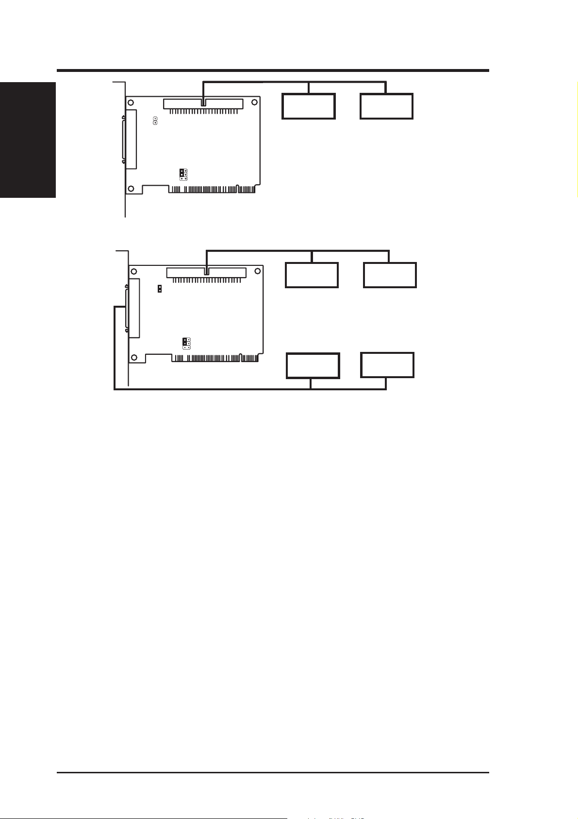
VI. ASUS SCSI Cards
(SCSI ID Numbers)
VI. ASUS PCI SCSI Cards
SCSI Device 1
SCSI Device 2
Termination Required
(JP5 Open)
No Termination Required
(JP5 Short)
SCSI Device 3
SCSI Device 2
Termination Required
(End Device)
SCSI Device 4
Termination Required
(End Device)
Termination Required
(End Device)
SCSI Device 1
SCSI ID Numbers for SCSI Devices
All SCSI devices, including the ASUS PCI-SC200 and ASUS PCI-SC860 interface
card must have a SCSI identification number that is not in use by any other SCSI
device. There are eight possible ID numbers, 0 through 7. The ASUS PCI-SC200 and
ASUS PCI-SC860 cards have fixed SCSI IDs of 7. The SCSI ID serves two purposes:
• It uniquely defines each SCSI device on the bus.
• It determines which device controls the bus when two or more devices try to use
it at the same time.
SCSI IDs on one channel do not interfere with the IDs on another channel. This applies to two SCSI host adapters that implement different buses as well as dual channels
on a single host adapter. You can connect up to seven SCSI devices to the interface
card. You must set a SCSI ID number (ID 0 to ID 6) for each device. SCSI devices
vary in how they set the ID number. Some use jumpers, others have some kind of
selector switch. Refer to the manual for any device you install for details on how to set
its ID number.
SCSI ID Priority
The ASUS PCI-SC200 and ASUS PCI-SC860 are 8bit single-channel SCSI cards.
SCSI ID 7 has the highest priority, and SCSI ID 0 has the lowest priority.
62 ASUS KN97 User’s Manual
Page 63
VII. ASUS I-A16C Audio Card
NOTE: The ASUS I-A16C 16-bit ISA audio card comes with certain motherboard bundles only and is not for sale separately.
ASUS I-A16C Audio Features
• Creative Labs ViBRA 16C PnP Audio Chip
• Full Duplex Supports
• 16/8-bit PCM 5KHz to 44.1KHz
• W ave Table Upgradeable
• Software Includes:
DOS and Window 3.1 Drivers
Windows 95 Driver
Wave Editor
Wave OLE
Quick CD
Mixer Control
Quick Player
VII. ASUS I-A16C
(Features/Precautions)
Unpacking and Handling Precautions
WARNING! Keep the ASUS I-A16C stored in its anti-static bag until you are ready
to install it in your system. The ASUS I-A16C is easily damaged by static electricity.
Observe the following precautions while unpacking and handling the board:
• Before handling the board, discharge static electricity from your body by touch-
ing an unpainted area of the system's metal chassis. While installing the board,
ground yourself frequently to discharge any static electricity that may accumulate in your body.
• After removing the board form the anti-static bag, place it on a grounded sur-
face with the components facing up.
• Check the board for damage. If any socketed component appears loose, press
firmly but carefully to seat the chip in its socket. Otherwise, avoid touching
the components on the board. Always handle the board by the edges.
ASUS KN97 User’s Manual 63
Page 64
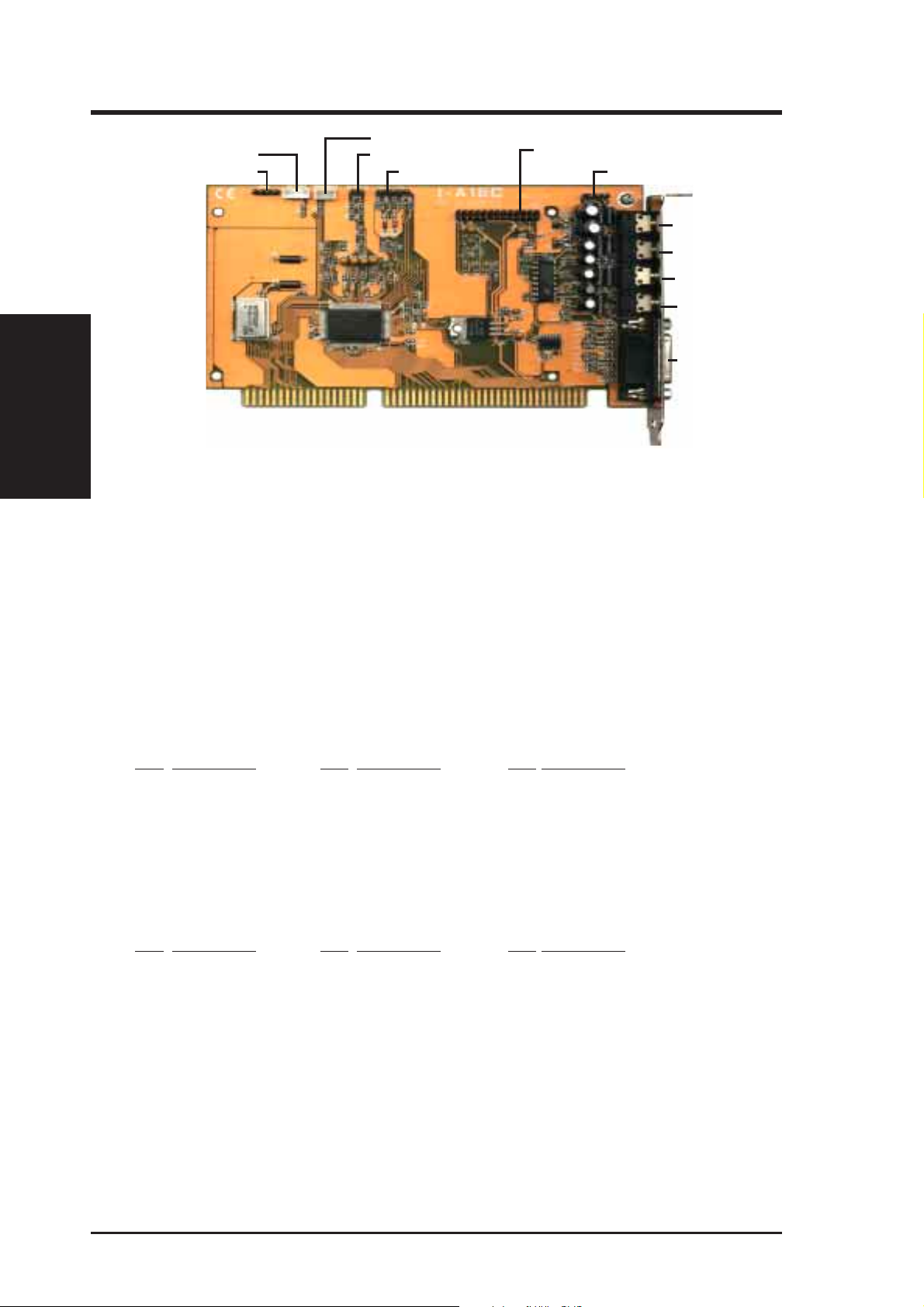
VII. ASUS I-A16C Audio Card
Mitsumi Audio In
Sony Audio In
(Layout / Connectors)
VII. ASUS I-A16C
Connectors
The audio input connectors are used when you wish to control software mixer settings (e.g., bass, treble, volume) for CDs that are played with your CD-ROM drive.
If the “Audio Out” from the CD-ROM drive is not connected to the “Audio In” on
the card, you can only use the direct output located in the front panel of the CDROM drive and adjust volume level by the knob.
Panasonic Audio In
PC Speaker In
Volume Control
Wave Table Upgrade
PC Speaker Out
Speaker Out
Line Out
Line In
Microphone
MIDI/Game
CD-Audio Connector Pin Definitions
Sony Audio In Mitsumi Audio In Panasonic Audio In
Pin Definition Pin Definition Pin Definition
l Right Signal 1 Ground 1 Left Signal
2 Ground 2 Left Signal 2 Ground
3 Ground 3 Ground 3 Right Signal
4 Left Signal 4 Right Signal -- ----
PC Speaker In PC Speaker Out Volume Control
Pin Definition Pin Definition Pin Definition
1 Mono Signal 1 Right Signal 1 Ground
2 Ground 2 Ground 2 Volume Up
-- ---- 3 Left Signal 3 Ground
-- ---- 4 Ground 4 Volume Down
-- ---- -- ---- 5 Ground
64 ASUS KN97 User’s Manual
 Loading...