

ASIX AX88875AP Datasheet

AX88875AP
ASIX
10/100BASE Dual Speed Bripeater Controller
ASIX AX88875AP
10/100BASE 5-Port
Dual Speed “Bripeater” Controller
Data Sheets (10/16/’00)
Always contact ASIX for possible updates
before starting a design.
DOCUMENT NO. : AX875A-06.DOC
This data sheets contain new products information. ASIX ELECTRONICS reserves the rights to modify the products
specification without notice. No liability is assumed as a result of the use of this product. No rights under any patent
accompany the sale of the product.
ASIX ELECTRONICS CORPORATION
2F, NO.13, Industry East Rd. II, Science-based Industrial Park, Hsin-Chu City, Taiwan, R.O.C.
TEL: 886-3-579-9500 FAX: 886-3-579-9558 http://www.asix.com.tw

AX88875AP Bripeater
CONTENTS
1.0 AX88875A OVERVIEW..................................................................................................................................... 3
1.1 GENERAL DESCRIPTION...................................................................................................................................... 3
1.2 FEATURES.......................................................................................................................................................... 4
1.3 BLOCK DIAGRAM............................................................................................................................................... 5
1.4 PIN CONNECTION DIAGRAM (MODE 0)................................................................................................................ 6
1.5 PIN CONNECTION DIAGRAM (MODE 1)................................................................................................................ 7
2.0 PIN DESCRIPTION........................................................................................................................................... 8
2.1 MII INTERFACES................................................................................................................................................ 8
2.2 LED DISPLAY.................................................................................................................................................... 9
2.3 BUFFER MEMORY PINS GROUP ........................................................................................................................... 10
2.4 MISCELLANEOUS.............................................................................................................................................. 11
2.5 POWER ON CONFIGURATION SETUP SIGNALS CROSS REFERENCE TABLE ................................................................ 12
3.0 FUNCTIONAL DESCRIPTION..................................................................................................................... 13
3.1 REPEATER STATE MACHINE.............................................................................................................................. 13
3.2 RXE /TXE CONTROL................................................................................................................................... 13
3.3 JABBER STATE MACHINE.................................................................................................................................. 14
3.4 PARTITION STATE MACHINE............................................................................................................................. 14
3.5 LED DISPLAY INTERFACE................................................................................................................................ 14
4.0 INTERNAL REGISTERS................................................................................................................................ 16
4.1 CONFIGURATION REGISTER (CONFIG)............................................................................................................. 16
5.0 ELECTRICAL SPECIFICATION AND TIMING.......................................................................................... 17
5.1 ABSOLUTE MAXIMUM RATINGS........................................................................................................................ 17
5.2 GENERAL OPERATION CONDITIONS................................................................................................................... 17
5.3 DC CHARACTERISTICS..................................................................................................................................... 17
5.4 AC SPECIFICATIONS......................................................................................................................................... 18
5.4.1 MII Interface Timing Tx & Rx.................................................................................................................. 18
5.4.2 SRAM read cycle and write cycle............................................................................................................. 19
5.4.3 LED DISPLAY ......................................................................................................................................... 20
5.4.4 LED Display After Reset.......................................................................................................................... 20
6.0 PACKAGE INFORMATION........................................................................................................................... 21
APPENDIX A: APPLICATIONS.......................................................................................................................... 22
A.1 STAND-ALONG 5-PORTS 10/100MBPS HUB APPLICATION................................................................................. 22
A.2 STAND-ALONG 4-PORTS 10/100MBPS HUB WITH ONE MAC APPLICATION........................................................ 22
APPENDIX B: USING MII I/F CONNECTS TO MAC...................................................................................... 23
FIGURES
FIG - 1 CHIP BLOCK DIAGRAM ..................................................................................................................................... 5
FIG - 2 PIN CONNECTION DIAGRAM (MODE 0) .............................................................................................................. 6
FIG - 3 PIN CONNECTION DIAGRAM (MODE 1) .............................................................................................................. 7
FIG - 4 APPLICATION FOR LED DISPLAY..................................................................................................................... 15
FIG - 5 STAND-ALONG 5-PORTS 10/100MBPS HUB APPLICATION ................................................................................ 22
FIG - 6 STAND-ALONG 4-PORTS 10/100MBPS HUB WITH ONE MAC APPLICATION ....................................................... 22
2
ASIX ELECTRONICS CORPORATION

AX88875AP Bripeater
1.0 AX88875A Overview
The AX88875A 10/100Mbps Dual Speed “Bripeater” Controller is “a dual speed
repeater with build in bridge function” It is design for low cost dumb HUB application. The
AX88875A directly supports up-to five 10/100Mbps automatic links MII interfaces specially for
SOHO market. The AX88875A is designed base on IEEE 802.3u clause 27 “ Repeater for
100Mb/s base-band networks” It is fully compatible with IEEE 802.3u standard.
1.1 General Description
The AX88875A Repeater Controller is a subset of a repeater set containing all the
repeater-specific components and functions, exclusive of PHY components and functions. The
AX88875A has five Media Independent Interfaces (MII) to connect to PHY or MAC devices.
The AX88875A supports 5 MII interfaces ports, a bridge packet buffer SRAM interface
and LED display interface. AX88875A without support expansion port to cascade to other
AX88850 and AX88860 pure 100Mbps repeater chips..
The AX88875A supports stand along 10/100Mbps dual speed repeater applications with
two LED display mode.
The AX88871A has two LED display mode.
Mode 0 Direct LED display mode.
Mode 1 Rich LED display mode.
3
ASIX ELECTRONICS CORPORATION

AX88875AP Bripeater
1.2 Features
• IEEE 802.3u repeater compatible
• Supports per port 10/100Mbps alternative with auto detected
• Build in 10/100Mbps bridge engine with following features
1. Minimum 32K bytes, maximum 128K bytes SRAM to buffer packets
2. Seamless buffer management without waste any space of buffer memory
3. Simple asynchronous 8-bit SRAM interface to reduce system cost
4. 256 or 1024 entries is supported
5. Auto learning and filtering
6. Two forwarding modes are supported : Store-n-Forward and fragment-free
7. Flow-control is supported optionally.
8. Buffer RAM auto testing
9. Routing and Learning at wire speed (148810 packets/sec at 100Mbps)
• Supports 5 10/100Mbps network connections
• 5 dedicated MII interfaces can support 100BASE-TX/T4/FX PHY interfaces
• 5th Port can connect to bridge, switch or MAC type device optionally.
• Low latency design supports Class II repeater implementation
• All ports can be separately isolated or partitioned in response to fault condition
• Separate jabber and partition state machines for each port
• Per-port LED display for Jabber, Partition, Activity. Global partition, RAM test fail and
collision, utilization (%) for 10/100Mbps presentation
• Power on LED diagnosis. All the LED display will follow the “ON-OFF-ON-OFF-Normal”
operation procedure during/after power on reset
• 160-pin PQFP
4
ASIX ELECTRONICS CORPORATION
AX88875AP Bripeater
MEM I/F
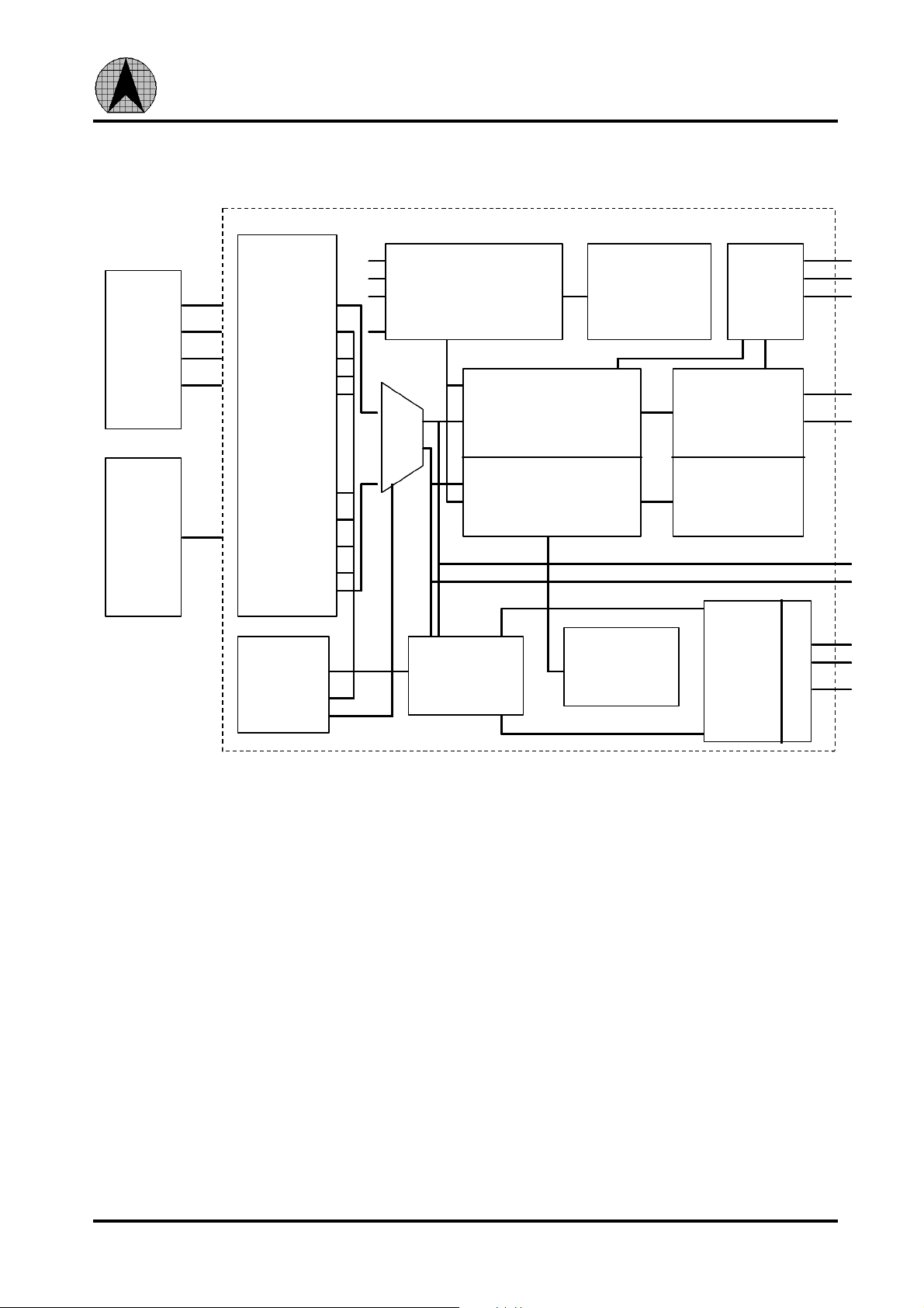
1.3 Block Diagram
MII
10/100
Q-PHY
I/F
MII
interface
Re-conciliation
Sub-layer
Per port Jabber ctl,
auto-partition SM &
Per port Collision ,
Partition counters.
........
MUX
Registers
Repeater State
Machine of 100Mbps
MIB I/F
(Reserved)
Cascade
Arbitration Logic
of 100Mbps
(Reserved)
10/100
PHY
or
MAC
MII
I/F
(Port 0 Port 4 )
Speed
Detection
circuit
Repeater State
Machine of 10Mbps
Elasticity Buffer
for 100Mbps
and 10Mbps
Fig - 1 Chip Block Diagram
Collision
Handling Logic
for 100Mbps
and10Mbps
(Reserved)
100Mbps
to
10Mbps
Bridge
5
ASIX ELECTRONICS CORPORATION

AX88875AP Bripeater
COL[2]
COL[1]
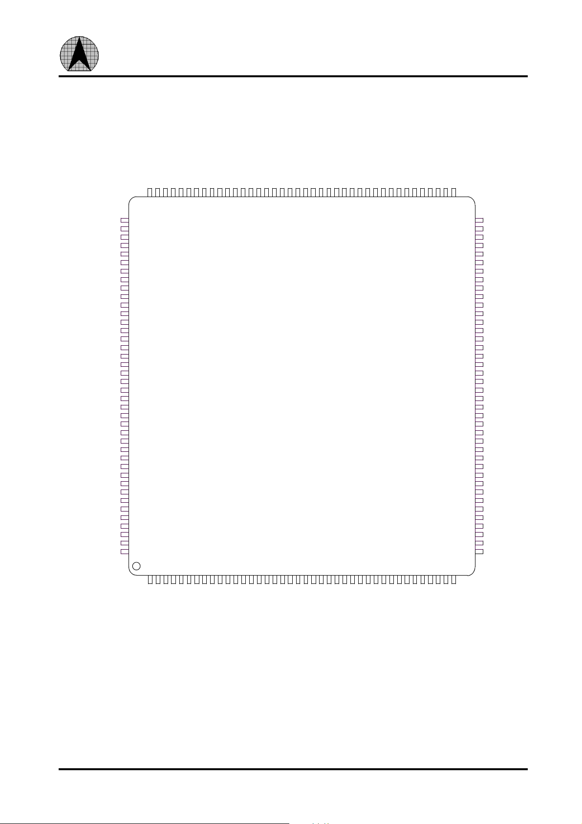
1.4 Pin Connection Diagram (Mode 0)
BMA[6]
BMA[7]
BMA[4]
VSS1
VDD1
109
108
13
12
107
14
106
BMA[5]
105
104
17
16
15
COL[0]
/LACT[4]
NC
/LACT[2]
/LACT[3]
VDD
NC
/LACT[0]
/LACT[1]
NC
TEST1
/RST
VSS
LCLK
/HALF10
VDD
PULL_DN
PULL_DN
VDD1
VSS1
RXER[0]
RXDV[0]
CRS[0]
RXCLK[0]
RXD[0][0]
RXD[0][1]
RXD[0][2]
RXD[0][3]
VSS
TXEN[0]
TXD[0][0]
TXD[0][1]
TXD[0][2]
TXD[0][3]
TXER[0]
RXER[1]
RXDV[1]
CRS[1]
RXCLK[1]
RXD[1][0]
RXD[1][1]
121
122
123
124
125
126
127
128
129
130
131
132
133
134
135
136
137
138
139
140
141
142
143
144
145
146
147
148
149
150
151
152
153
154
155
156
157
158
159
160
/LPART[4]
VSS
/LPART[3]
120
118
117
119
2
3
1
/LUTI[4]
/LPART[2]
/LPART[0]
/TEST2
/LPART[1]
115
116
113
114
4
5
8
6
7
/LCOL10
/LSEL10
/LUTI[5]
110
112
111
AX88875AP
( Mode 0 )
9
11
10
BMA[3]
VDD
102
103
19
18
BMA[2]
BMA[0]
BMA[1]
99
101
100
22
20
21
BMD[7]
VSS
96
97
98
24
23
BMD[4]
BMD[5]
BMD[6]
95
94
25
26
27
BMD[2]
BMD[1]
BMD[3]
93
91
92
29
28
30
BMD[0]
BMA[16]
VSS
88
90
89
31
32
33
BMA[12]
BMA[15]
BMA[14]
BMA[13]
84
86
85
87
35
37
34
36
BMA[10]
BMA[11]
VDD
81
83
82
80
79
78
77
76
75
74
73
72
71
70
69
68
67
66
65
64
63
62
61
60
59
58
57
56
55
54
53
52
51
50
49
48
47
46
45
44
43
42
41
38
39
40
BMA[9]
BMA[8]
/BMWR
/LUTI[3]
/LUTI[2]
/LUTI[1]
/LUTI[0]
/BMA[15]
MCLK
MDO
MDC
/LCOL100
VSS
COL_O[4]
TXER[4]
TXD[4][3]
TXD[4][2]
TXD[4][1]
TXD[4][0]
TXEN[4]
RXD[4][3]
RXD[4][2]
RXD[4][1]
RXD[4][0]
RXCLK[4]
VDD1
VSS1
CRS[4]
RXDV[4]
RXER[4]
VDD
SET2
SET1
SET0
PULL_DN
VSS
TXER[3]
TXD[3][3]
TXD[3][2]
TXD[3][1]
COL[4]
COL[3]
VDD
RXD[1][2]
RXD[1][3]
TXEN[1]
TXD[1][2]
TXD[1][1]
TXD[1][0]
VSS
TXER[1]
PULL_DN
TXD[1][3]
VSS1
VDD1
RXER[2]
PULL_DN
CRS[2]
RXDV[2]
RXD[2][0]
RXCLK[2]
TXEN[2]
RXD[2][1]
RXD[2][2]
RXD[2][3]
TXD[2][1]
TXD[2][0]
VSS
TXER[2]
TXD[2][3]
TXD[2][2]
CRS[3]
RXER[3]
RXDV[3]
RXCLK[3]
Fig - 2 Pin Connection Diagram (Mode 0)
Note : Power on configuration setup signals refer section 2.5 cross referance table
6
ASIX ELECTRONICS CORPORATION
RXD[3][0]
RXD[3][1]
RXD[3][3]
RXD[3][2]
VDD
TXEN[3]
TXD[3][0]
AX88875AP Bripeater
COL[2]
COL[1]
1.5 Pin Connection Diagram (Mode 1)
COL[0]
NC
NC
NC
NC
VDD
NC
NC
NC
NC
TEST1
/RST
VSS
LCLK
/HALF10
VDD
PULL_DN
PULL_DN
VDD1
VSS1
RXER[0]
RXDV[0]
CRS[0]
RXCLK[0]
RXD[0][0]
RXD[0][1]
RXD[0][2]
RXD[0][3]
VSS
TXEN[0]
TXD[0][0]
TXD[0][1]
TXD[0][2]
TXD[0][3]
TXER[0]
RXER[1]
RXDV[1]
CRS[1]
RXCLK[1]
RXD[1][0]
RXD[1][1]
121
122
123
124
125
126
127
128
129
130
131
132
133
134
135
136
137
138
139
140
141
142
143
144
145
146
147
148
149
150
151
152
153
154
155
156
157
158
159
160
VSS
120
1
NC
119
2
NC
118
3
NCNCNC
NC
/TEST2
117
115
116
114
4
5
7
6
BMA[1]
BMA[2]
BMA[3]
102
101
BMA[0]
99
100
NC
NC
/LCOL10
111
112
110
113
VSS1
VDD1
109
108
BMA[7]
BMA[5]
BMA[6]
105
107
106
BMA[4]
VDD
103
104
AX88875AP
( Mode 1 )
8
9
12
10
13
11
14
15
16
17
18
19
20
21
VSS
98
22
BMD[6]
BMD[7]
96
97
24
23
BMD[5]
BMD[4]
94
95
26
25
BMD[3]
93
27
28
BMD[2]
BMD[0]
BMD[1]
90
91
92
30
29
31
BMA[15]
BMA[16]
VSS
87
88
89
33
34
32
BMA[12]
BMA[14]
BMA[13]
BMA[11]
83
84
86
85
37
35
36
38
BMA[10]
VDD
81
82
80
79
78
77
76
75
74
73
72
71
70
69
68
67
66
65
64
63
62
61
60
59
58
57
56
55
54
53
52
51
50
49
48
47
46
45
44
43
42
41
40
39
BMA[9]
BMA[8]
/BMWR
LED_CK
LED[2]
LED[1]
LED[0]
/BMA[15]
MCLK
MDO
MDC
/LCOL100
VSS
COL_O[4]
TXER[4]
TXD[4][3]
TXD[4][2]
TXD[4][1]
TXD[4][0]
TXEN[4]
RXD[4][3]
RXD[4][2]
RXD[4][1]
RXD[4][0]
RXCLK[4]
VDD1
VSS1
CRS[4]
RXDV[4]
RXER[4]
VDD
SET2
SET1
SET0
PULL_DN
VSS
TXER[3]
TXD[3][3]
TXD[3][2]
TXD[3][1]
COL[4]
COL[3]
VDD
RXD[1][3]
RXD[1][2]
TXEN[1]
TXD[1][2]
TXD[1][0]
TXD[1][1]
VSS
TXER[1]
TXD[1][3]
PULL_DN
VSS1
VDD1
RXER[2]
PULL_DN
CRS[2]
RXDV[2]
RXCLK[2]
RXD[2][0]
TXEN[2]
RXD[2][3]
RXD[2][2]
RXD[2][1]
TXD[2][1]
TXD[2][0]
VSS
TXER[2]
TXD[2][2]
TXD[2][3]
RXER[3]
RXDV[3]
Fig - 3 Pin Connection Diagram (Mode 1)
Note : Power on configuration setup signals refer section 2.5 cross referance table
7
ASIX ELECTRONICS CORPORATION
CRS[3]
RXCLK[3]
RXD[3][0]
RXD[3][1]
VDD
TXEN[3]
RXD[3][2]
RXD[3][3]
TXD[3][0]
 Loading...