

ASIX AX88873P Datasheet
10/100BASE Dual Speed Repeater Controller
Features
100Mbps horizontal cascade
10Mbps and 100Mbps Vertical cascade upto 4 stacks
10Mbps horizontal cascade
2 Quad RMII PHY
2 Quad RMII PHY
2 Quad RMII PHY
PHY for Up-link
PHY for Down-link or Server
AX88873P
10/100BASE Dual Speed 8-Port Repeater
Ver. 1.1
• IEEE 802.3u repeater compatible
• Supports 8 10/100Mbps RMII I/F repeater ports
• Accompany with AX88872 to build a low cost dual
speed repeater solution
• Up-to 4 repeaters can be cascaded for vertical
expansion
• Up-to 3 chips can be cascaded locally for horizontal
expansion
• All ports can be separately isolated or partitioned in
response to fault condition
• Separate jabber and partition state machines for
each port
• Per-port LED display for Jabber, Partition, Activity
and global collision, utilization (%) for
10/100Mbps presentation
• Power on LED diagnosis. All the LED display will
follow the “ON-OFF-ON-OFF-Normal” operation
procedure during/after power on reset
• 50MHz Operation, 3.3volt and 128-pin PQFP
Product description
The AX88873 10/100Mbps Dual Speed repeater Controller is a counterpart of AX88872 without built in 4-ports
switch. It is design for low cost dual speed dumb HUB application.
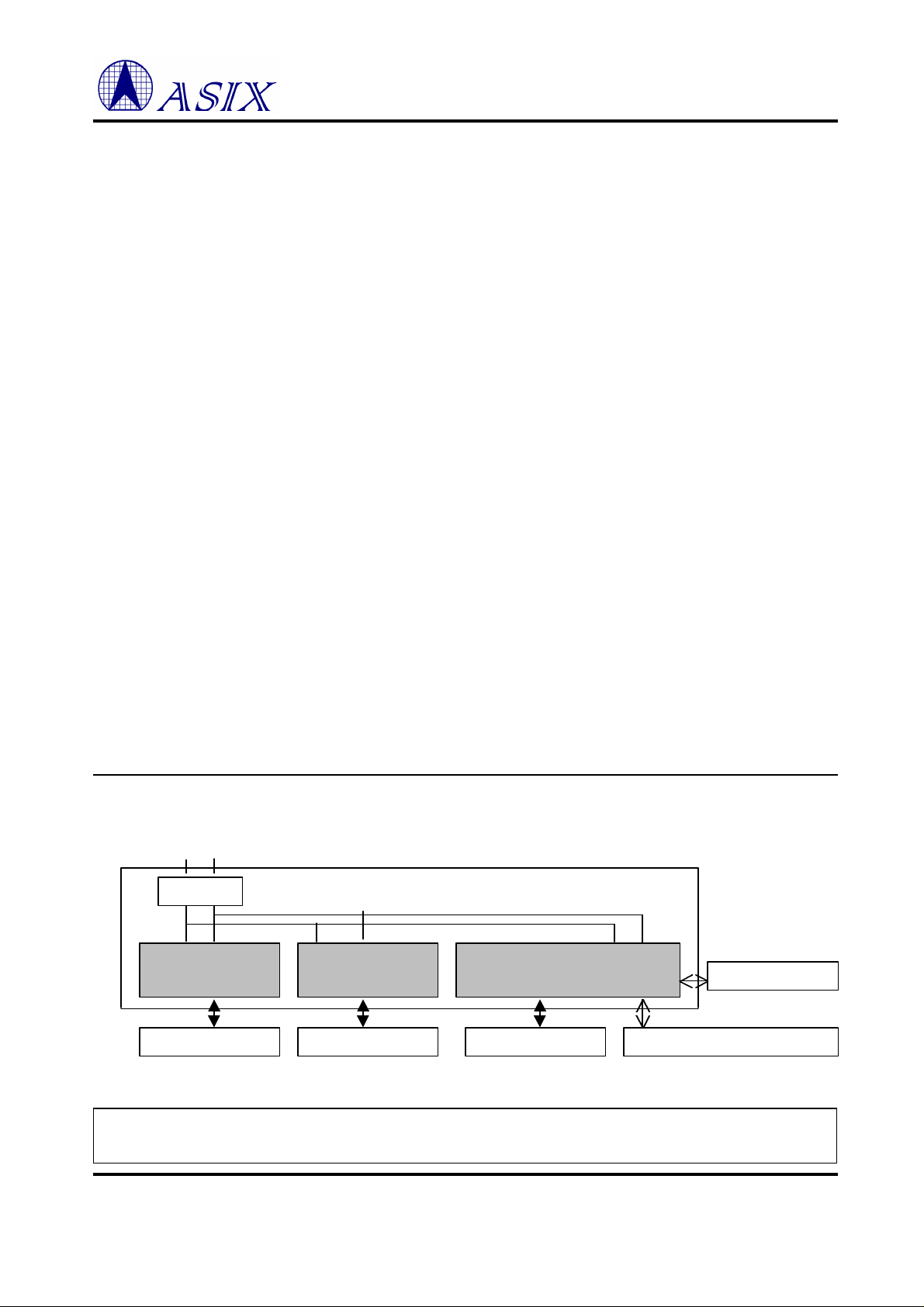
The AX88873 directly supports up-to eight 10/100Mbps automatic links RMII interfaces. Maximum up-to 96
repeater ports can be constructed by stacking 1 AX88872 and 2 AX88873 chips horizontally and then cascading 4
horizontal boards vertically.
With using 128-pin low cost package, accompany with AX88872 to build up low cost dual speed repeater application.
Not only perform the repeater function but gain additional 2 switch ports. The 2 dual speed switch ports are connected
to external MII or RMII interfaces PHY for various applications. For example, one port is use for down link and the
other is used for up link to extend the network topology. The other case is one port for up link and the other port for
server.
The AX88873 is designed base on IEEE 802.3u clause 27 “ Repeater for 100Mb/s base-band networks” It is fully
compatible with IEEE 802.3u standard. Please refer Ax872-11.doc to get more information about AX88872.
System Block Diagram
Buffer
AX88873 #1
Repeater Controller
Always contact ASIX for possible updates before starting a design.
This data sheet contains new products information. ASIX ELECTRONICS reserves the rights to modify product specification without notice. No liability
is assumed as a result of the use of this product. No rights under any patent accompany the sale of the product.
AX88873 #0
Repeater Controller
AX88872 #0
Swipeater Controller
ASIX ELECTRONICS CORPORATION Doc. No. AX873-11.DOC Date : APR/26/1999
2F, NO.13, Industry East Rd. II, Science-based Industrial Park, Hsin-Chu City, Taiwan, R.O.C.
TEL: 886-3-579-9500 FAX: 886-3-579-9558 http://www.asix.com.tw

CONFIDENTIAL
AX88873P 10/100Mb Repeater Controller PRELIMINARY
CONTENTS
1.0 AX88873 OVERVIEW....................................................................................................................................... 4
1.1 GENERAL DESCRIPTION...................................................................................................................................... 4
1.2 AX88873 BLOCK DIAGRAM:.............................................................................................................................. 4
1.3 PIN CONNECTION DIAGRAM ............................................................................................................................... 5
2.0 PIN DESCRIPTION........................................................................................................................................... 6
2.1 RMII INTERFACE FOR REPEATER PORTS............................................................................................................... 6
2.1.1 Repeater Port 0 .......................................................................................................................................... 6
2.1.2 Repeater Port 1 .......................................................................................................................................... 6
2.1.3 Repeater Port 2 .......................................................................................................................................... 7
2.1.4 Repeater Port 3 .......................................................................................................................................... 7
2.1.5 Repeater Port 4 .......................................................................................................................................... 7
2.1.6 Repeater Port 5 .......................................................................................................................................... 7
2.1.7 Repeater Port 6 .......................................................................................................................................... 8
2.1.8 Repeater Port 7 .......................................................................................................................................... 8
2.2 EXPANSION BUS INTERFACE FOR 100 MBPS......................................................................................................... 8
2.3 EXPANSION BUS INTERFACE FOR 10 MBPS........................................................................................................... 9
2.4 LED DISPLAY.................................................................................................................................................. 10
2.5 MISCELLANEOUS.............................................................................................................................................. 10
2.6 POWER ON CONFIGURATION SETUP SIGNALS CROSS REFERENCE TABLE ................................................................ 11
3.0 FUNCTIONAL DESCRIPTION..................................................................................................................... 12
3.1 REPEATER STATE MACHINE.............................................................................................................................. 12
3.2 RXE /TXE CONTROL...................................................................................................................................... 12
3.3 JABBER STATE MACHINE.................................................................................................................................. 12
3.4 PARTITION STATE MACHINE............................................................................................................................. 12
3.5 LED DISPLAY INTERFACE................................................................................................................................ 13
4.0 INTERNAL REGISTERS................................................................................................................................ 14
5.0 ELECTRICAL SPECIFICATION AND TIMING.......................................................................................... 15
5.1 ABSOLUTE MAXIMUM RATINGS........................................................................................................................ 15
5.2 GENERAL OPERATION CONDITIONS................................................................................................................... 15
5.3 DC CHARACTERISTICS..................................................................................................................................... 15
5.4 AC SPECIFICATIONS......................................................................................................................................... 16
5.4.1 RMII Interface Timing TX & RX............................................................................................................... 16
5.4.2 MII Interface Timing TX & RX................................................................................................................. 17
5.4.3 LED DISPLAY ......................................................................................................................................... 18
5.4.4 LED Display after Reset........................................................................................................................... 18
6.0 PACKAGE INFORMATION........................................................................................................................... 19
APPENDIX A: APPLICATIONS.......................................................................................................................... 20
A.1 16-PORT (24-PORT) REPEATER WITH 2-PORT SWITCH......................................................................................... 20
A.2 16-PORT REPEATER WITH UPTO 4 STACKS ......................................................................................................... 20
A.3 16-PORT REPEATER WITH UPTO 4 STACKS UP-LINK TO EXTERNAL SWITCH........................................................... 21
2
ASIX ELECTRONICS CORPORATION

CONFIDENTIAL
AX88873P 10/100Mb Repeater Controller PRELIMINARY
FIGURES
FIG - 1 AX88873 BLOCK DIAGRAM ............................................................................................................................. 4
FIG - 2 PIN CONNECTION DIAGRAM..............................................................................................................................5
FIG - 3 APPLICATION FOR LED DISPLAY..................................................................................................................... 13
3
ASIX ELECTRONICS CORPORATION
CONFIDENTIAL
AX88873P 10/100Mb Repeater Controller PRELIMINARY
1.0 AX88873 Overview
1.1 General Description
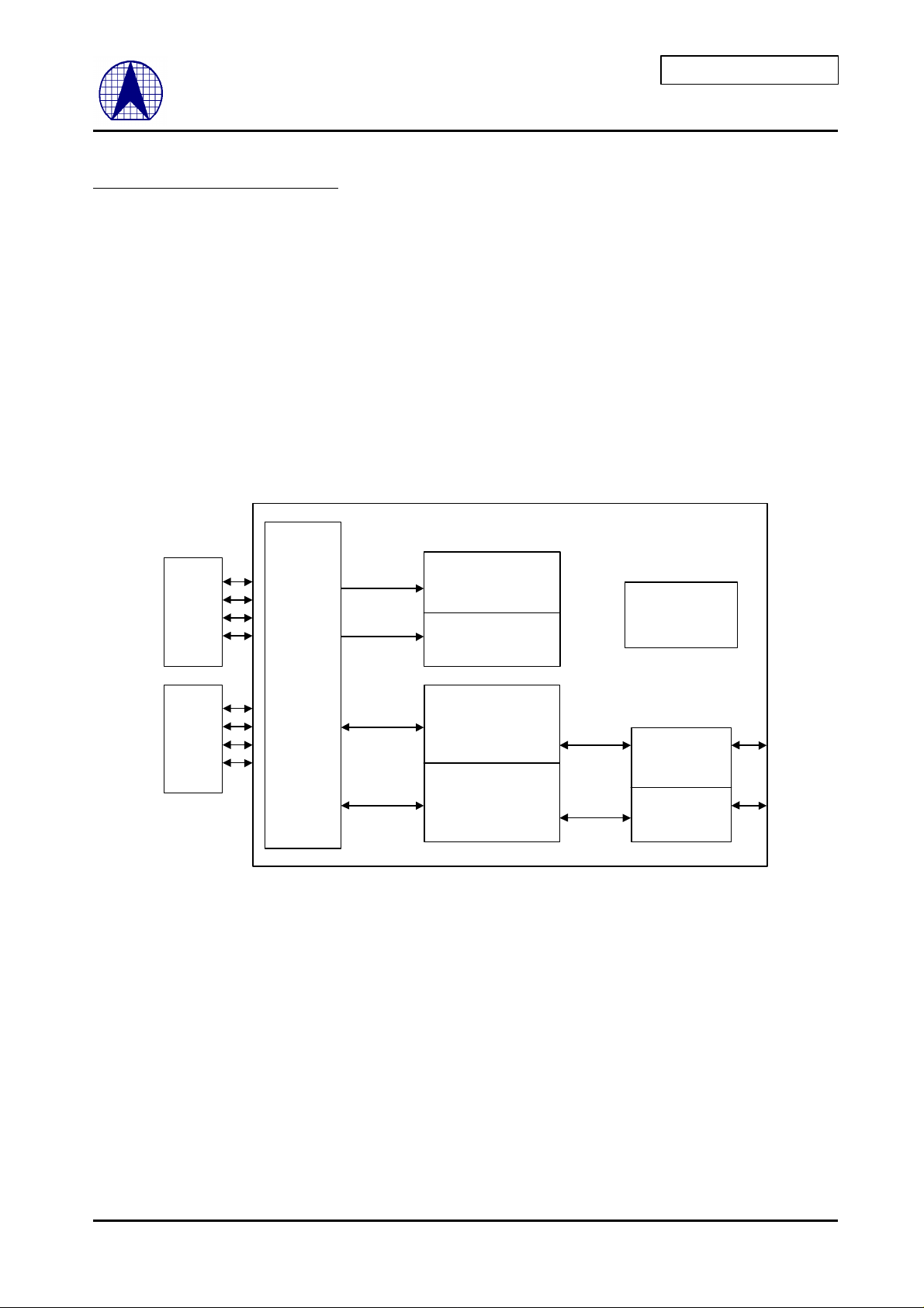
The AX88873 is a simple dual speed repeater that provides two expansion buses for 10M and 100M
segments respectively. Accompany with AX88872 (build-in a 4-port switch) can construct high port
count (16 ports or 24 ports) application and gain 2 additional switch ports. Additional two switch
ports are also useful for up-link or connection of server.
The pin count of chip is reduced to 128 when design uses RMII I/F instead of MII. It is not only
simplify the design but also user can choose low cost RMII Quad PHY.
1.2 AX88873 Block Diagram:
RMII
I/F
10/100
Q-PHY
RMII /MII
translation
for Repeater
Port 0 -7
10/100
Q-PHY
Per Port Jabber
Detection
Per Port Partition
Detection
Repeater State
Machine of 100Mbps
Repeater State
Machine of 10Mbps
Led Interface
Cascade
Arbitration Logic
of 100Mbps
Cascade
Arbitration Logic
of 10Mbps
Fig - 1 AX88873 Block Diagram
4
ASIX ELECTRONICS CORPORATION
CONFIDENTIAL
AX88873P 10/100Mb Repeater Controller PRELIMINARY
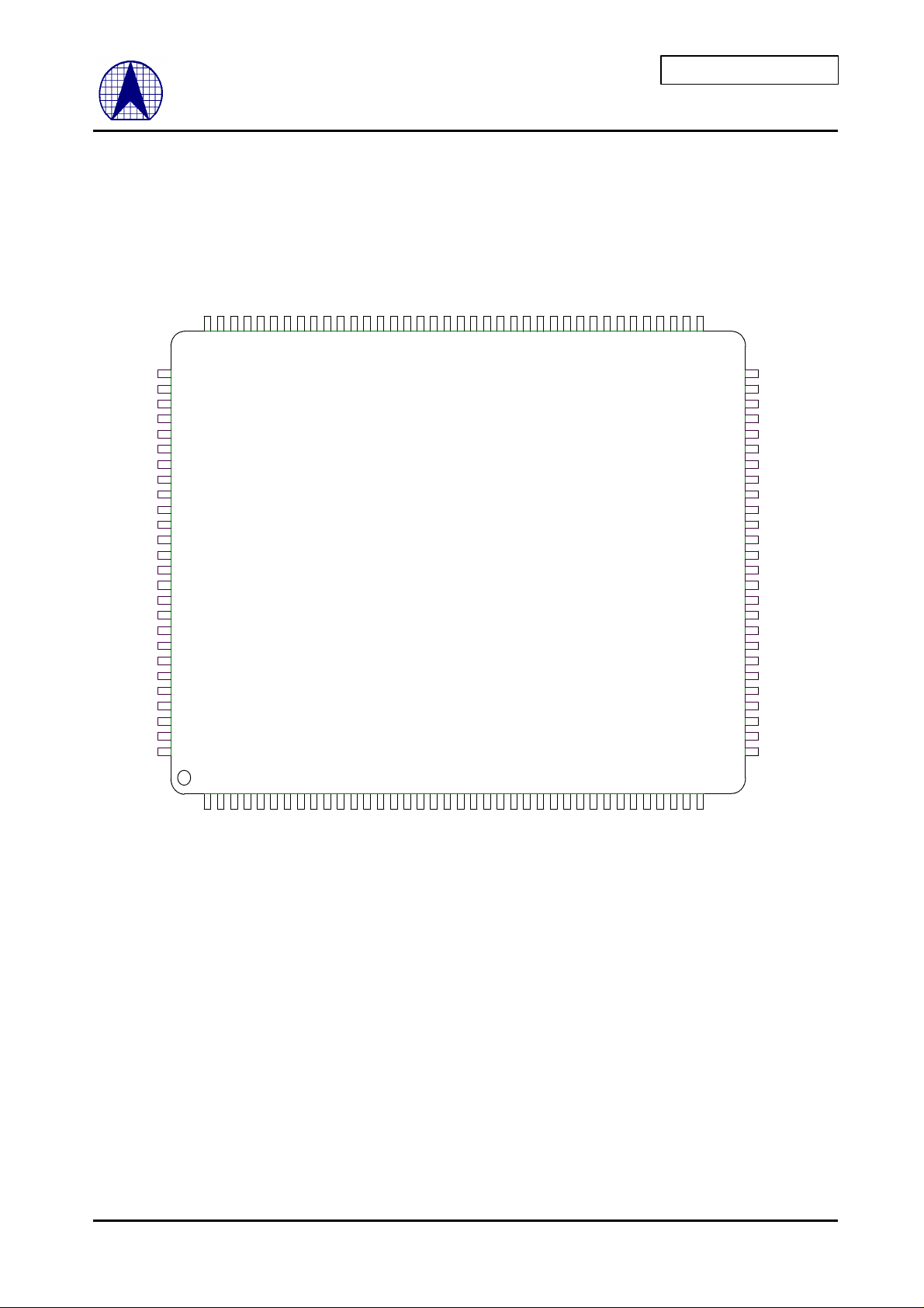
1.3 Pin Connection Diagram
VSS
TXD5[1]
RXD5[1]
TXD5[0]
TXEN5
CRS_DV5
RXD5[0]
CRS_DV6
RXD6[1]
RXD6[0]
TXD6[0]
TXD6[1]
TXEN6
CRS_DV7
RXD7[1]
RXD7[0]
NC
NC
VDD
SPEED5
SPEED6
SPEED7
VSS
SPEED4
RXD4[1]
TXEN4
TXD4[0]
TXD4[1]
RXD4[0]
CRS_DV4
TXD3[1]
TXD3[0]
TXEN3
RXD3[1]
CRS_DV3
RXD3[0]
VDD
SPEED3
HIRD[2]
HIRD[3]
NC
/HIRD_V
HIRD[0]
HIRD[1]
/HIR_ACTO[3]
HIRD_CK
HIRD_ODIR
VSS
/HIR_ACTI[3]
NC
/HIR_ACTO[0]
/HIR_ACTO[1]
/HIR_ACTO[2]
/HIR_ACTI[2]
VDD
/HIR_ACTI[0]
/HIR_ACTI[1]
/LHIR_ACT[2]
/LHIR_ACT[0]
/LHIR_ACT[1]
VSS
/TIR_ACTI[2]
/TIR_ACTO[1]
/TIR_ACTI[3]
/TIR_ACTO[0]
/TIR_ACTO[2]
/TIR_ACTO[3]
VDD
VSS
/TIR_ACTI[0]
/TIR_ACTI[1]
/LTIR_ACT[1]
/LTIR_ACT[2]
VSS
/LTIR_ACT[0]
TIRD[3]
SPEED0
CRS_DV0
RXD0[0]
RXD0[1]
VDD
TXEN0
TXD0[0]
TXD0[1]
SPEED1
VSS
CRS_DV1
RXD1[0]
RXD1[1]
TXEN1
VSS
TXD1[0]
TXD1[1]
VDD
SPEED2
CRS_DV2
RXD2[0]
RXD2[1]
TXEN2
TXD2[0]
TXD2[1]
VSS
103
104
105
106
107
108
109
110
111
112
113
114
115
116
117
118
119
120
121
122
123
124
125
126
127
128
102
1
101
2
100
3
78
75
77
797480
84
829181
93
94
95
96
989799
90
86
87
8892858983
76
AX88873
8
7
4
6
5
9
10
11
12
13
14
15
16
17
18
19
20
21
22
23
24
25
26
27
28
29
73
30
72
31
71
32
70
33
69
34
68
35
67
36
66
37
65
38
64
63
62
61
60
59
58
57
56
55
54
53
52
51
50
49
48
47
46
45
44
43
42
41
40
39
TIRD[2]
TIRD[1]
TIRD[0]
VSS
/TIRD_V
TIRD_CK
TIRD_ODIR
VDD
LED_CK
LED<1>
LED<0>
VSS
DAISY_OUT
DAISY_IN
VSS
NC
VDD
REF_CLK
VSS
/RST
/TEST
MDO
MDC
TXD7[1]
TXD7[0]
TXEN7
Fig - 2 Pin Connection Diagram
5
ASIX ELECTRONICS CORPORATION
CONFIDENTIAL
AX88873P 10/100Mb Repeater Controller PRELIMINARY
2.0 Pin Description
The following terms describe the AX88873 pin out:
All pin names with the “/” suffix are asserted low.
I = Input
O = Output
I/O = Input /Output
2.1 RMII interface for repeater ports
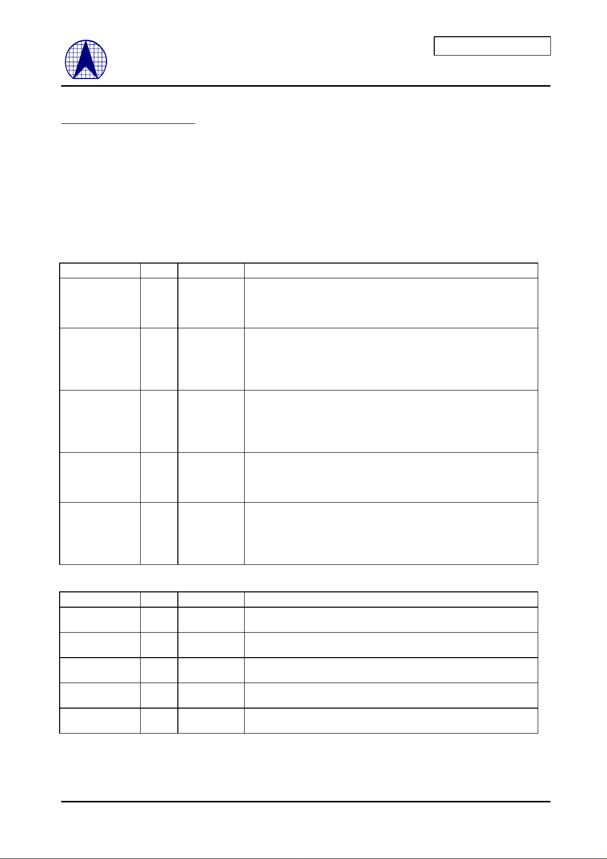
2.1.1 Repeater Port 0
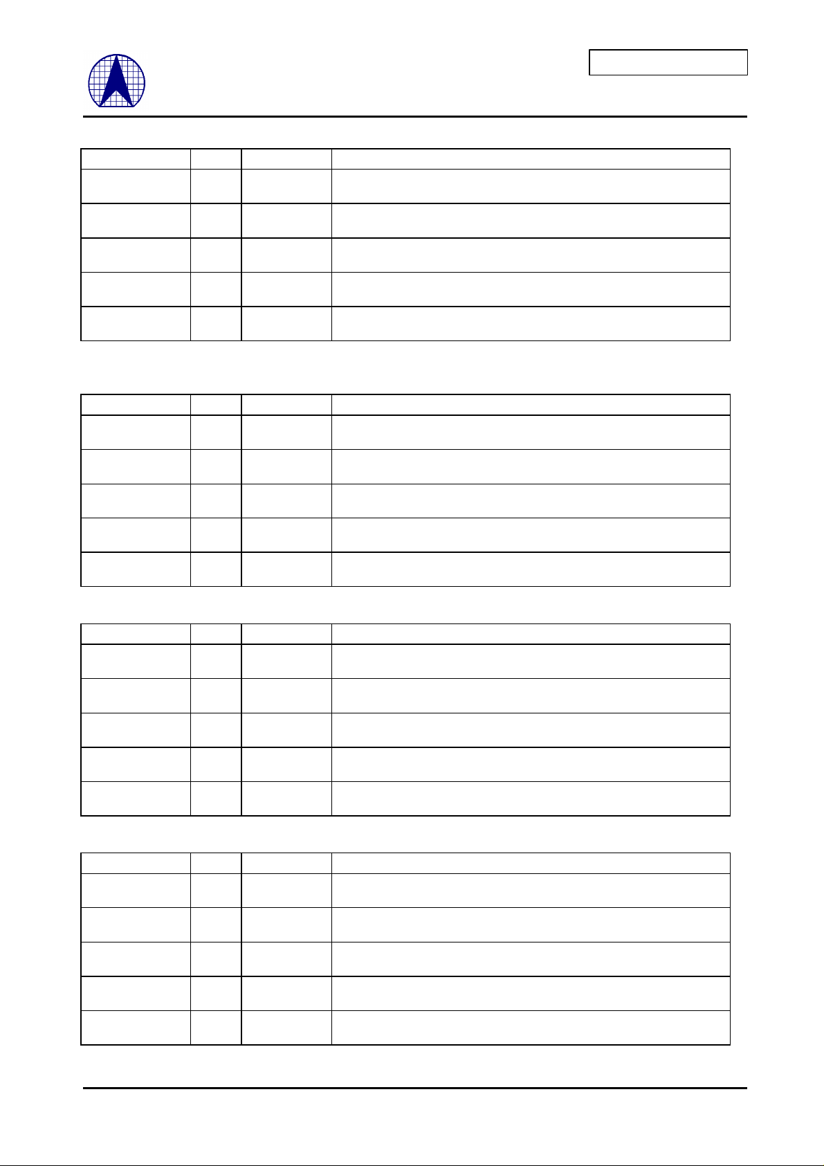
Signal Name Type Pin No. Description
SPEED0 I 103
CRS_DV0 I 104
RXD0[1:0] I 106,105
TXEN0 O 108
TXD0[1:0] O 110,109
Speed Select : SPEED0 is not standard RMII signal. This signal is
sourced from PHY to inform repeater whether 10M or 100M speed is
auto-negociated. Active for 10Mbps speed is selected depending on
power on configuration.
Carrier Sense/Receive Data Valid : CRS_DV is asserted
asynchronously on detection of carrier. CRS_DV is asserted by the PHY
when receive medium is non-idle. Loss of carrier shall result in the
desertion of CRS_DV synchronous to the cycle of REF_CLK, which
presents the first DI-bit of a nibble on to RXD0[1:0].
Receive Data : RXD0[1:0] is synchronous to REF_CLK
RXD0[1:0] shall be “00” to indicate idle when CRS_DV is disserted.
Value other than “00” are reserved for out-of-band signaling shall be
ignored by MAC Upon assertion of CRS_DV, PHY shall ensure that
RXD[1:0] = “00” until proper receive decoding takes place
Transmit Enable : TXEN0 is synchronous to REF_CLK.
TXEN0 indicates that MAC is presenting DI-bits on TXD[1:0] for
transmission. TXEN0 shall be negated prior to the 1st REF_CLK rising
edge following the final DI-bit of a frame
Transmit Data : TXD0[1:0] shall transition synchronously to
REF_CLK. TXD0[1:0] shall be “00” to indicate idle when TX_EN is
disserted. Value other than “00” are reserved for out-of-band signaling
shall be ignored by PHY. When TX_EN is asserted, TXD[1:0] are
accepted for transmission by PHY
2.1.2 Repeater Port 1
Signal Name Type Pin No. Description
SPEED1 I 111
CRS_DV1 I 113
RXD1[1:0] I 115,114
TXEN1 O 116
TXD1[1:0] O 119,118
Speed Select : Please references section 2.1.1 PORT0 description.
Carrier Sense/Receive Data Valid : Please references section 2.1.1
PORT0 description.
Receive Data : Please references section 2.1.1 PORT0 description.
Transmit Enable : Please references section 2.1.1 PORT0 description.
Transmit Data : Please references section 2.1.1 PORT0 description.
6
ASIX ELECTRONICS CORPORATION
CONFIDENTIAL
AX88873P 10/100Mb Repeater Controller PRELIMINARY
2.1.3 Repeater Port 2
Signal Name Type Pin No. Description
SPEED2 I 121
Speed Select : Please references section 2.1.1 PORT0 description.
CRS_DV2 I 122
RXD2[1:0] I 124,123 Receive Data : Please references section 2.1.1 PORT0 description.
TXEN2 O 125
TXD2[1:0] O 127,126
Carrier Sense/Receive Data Valid : Please references section 2.1.1
PORT0 description.
Transmit Enable : Please references section 2.1.1 PORT0 description.
Transmit Data : Please references section 2.1.1 PORT0 description.
2.1.4 Repeater Port 3
Signal Name Type Pin No. Description
SPEED3 I 1
CRS_DV3 I 2
RXD3[1:0] I 4,3
TXEN3 O 5
TXD3[1:0] O 7,6
Speed Select : Please references section 2.1.1 PORT0 description.
Carrier Sense/Receive Data Valid : Please references section 2.1.1
PORT0 description.
Receive Data : Please references section 2.1.1 PORT0 description.
Transmit Enable : Please references section 2.1.1 PORT0 description.
Transmit Data : Please references section 2.1.1 PORT0 description.
2.1.5 Repeater Port 4
Signal Name Type Pin No. Description
SPEED4 I 9
CRS_DV4 I 10
RXD4[1:0] I 12,11
TXEN4 O 13
TXD4[1:0] O 15,14
Speed Select : Please references section 2.1.1 PORT0 description.
Carrier Sense/Receive Data Valid : Please references section 2.1.1
PORT0 description.
Receive Data : Please references section 2.1.1 PORT0 description.
Transmit Enable : Please references section 2.1.1 PORT0 description.
Transmit Data : Please references section 2.1.1 PORT0 description.
2.1.6 Repeater Port 5
Signal Name Type Pin No. Description
SPEED5 I 19
CRS_DV5 I 20
RXD5[1:0] I 23,22
TXEN5 O 24
Speed Select : Please references section 2.1.1 PORT0 description.
Carrier Sense/Receive Data Valid : Please references section 2.1.1
PORT0 description.
Receive Data : Please references section 2.1.1 PORT0 description.
Transmit Enable : Please references section 2.1.1 PORT0 description.
TXD5[1:0] O 26,25
Transmit Data : Please references section 2.1.1 PORT0 description.
7
ASIX ELECTRONICS CORPORATION
 Loading...