

ASIX AX88190AL Datasheet
Features
DAA
MAGNETIC
EEPROM
MAGNETIC
RJ11 or BNC
AX88190AL
PCMCIA Fast Ethernet MAC Controller
10/100BASE PCMCIA Fast Ethernet MAC Controller
Document No.: AX190A-13 / V1.3 / June. 27 ’00
• IEEE 802.3u 100BASE-T, TX, and T4 Compatible
• Single chip PCMCIA bus 10/100Mbps Fast
Ethernet MAC Controller
• Embedded 8K * 16 bit SRAM
• NE2000 register level compatible instruction
• Compliant with 16 bit PC Card Standard - February
1995
• Support both 10Mbps and 100Mbps data rate
• Support both full-duplex or half-duplex operation
• Provides a MII port for both 10/100Mbps operation
• Provides SNI I/F for Home LAN PHY or 10M
transceiver option
• Support 128/256 bytes EEPROM (used for saving
CIS)
• Support automatic loading of Ethernet ID, CIS and
Adapter Configuration from EEPROM on power-on
initialization
• External and internal loop-back capability
• Support 8 General Purpose I/O ports
• 128-pin LQFP low profile package
• 20MHz to 25MHz Operation, Dual 5V and 3.3V
CMOS process with 5V I/O tolerance. Or pure 3.3V
operation
*IEEE is a registered trademark of the Institute of
Electrical and Electronic Engineers, Inc.
*All other trademarks and registered trademark are the
property of their respective holders.
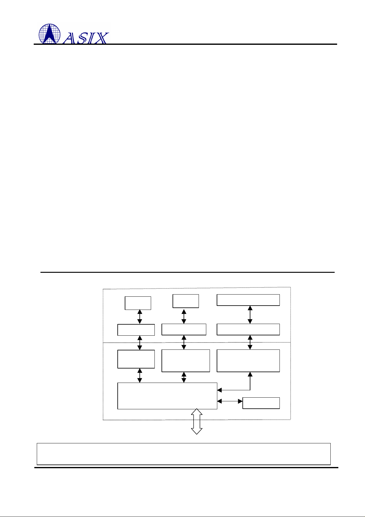
Product description
The AX88190A Fast Ethernet Controller is a high performance and highly integrated PCMCIA bus Ethernet Controller
with embedded 8K*16 bit SRAM. The AX88190A contains a 16 bit PCMCIA interfaces to host CPU and compliant with
PC Card Standard – February 1995. The AX88190A implements both 10Mbps and 100Mbps Ethernet function based on
IEEE802.3 / IEEE802.3u LAN standard. The AX88190A supports 10Mbps/100Mbps media-independent interface (MII)
and legacy pure 10Mbps SNI interface to simplify the design. Using Serial Network Interface (SNI) transceiver, Home
LAN PHY or 10BASE-2 BNC type media can be supported. The AX88190A is built in interface to connect
FAX/MODEM chipset with parallel bus interface.
System Block Diagram
RJ11
MODEM
AX88190A
RJ45
10/100
PHY/TxRx
Home LAN PHY or
10M PHY/TxRx
PCMCIA I/F
This data sheet contains new products information. ASIX ELECTRONICS reserves the rights to modify product specification without notice. No liability
is assumed as a result of the use of this product. No rights under any patent accompany the sale of the product.
Always contact ASIX for possible updates before starting a design.
ASIX ELECTRONICS CORPORATION Frist Released Date : Dec/13/1999
2F, NO.13, Industry East Rd. II, Science-based Industrial Park, Hsin-Chu City, Taiwan, R.O.C.
TEL: 886-3-579-9500 FAX: 886-3-579-9558 http://www.asix.com.tw

AX88190A PCMCIA Fast Ethernet MAC Controller
CONTENTS
1.0 INTRODUCTION...............................................................................................................................................5
1.1 GENERAL DESCRIPTION: ..................................................................................................................................... 5
1.2 AX88190A BLOCK DIAGRAM:............................................................................................................................5
1.3 AX88190A PIN CONNECTION DIAGRAM ............................................................................................................. 6
2.0 SIGNAL DESCRIPTION.................................................................................................................................... 7
2.1 PCMCIA BUS INTERFACE SIGNALS GROUP .........................................................................................................7
2.2 EEPROM SIGNALS GROUP.................................................................................................................................8
2.3 MII INTERFACE SIGNALS GROUP ..........................................................................................................................8
2.4 SNI INTERFACE PINS GROUP................................................................................................................................9
2.5 MODEM INTERFACE PINS GROUP .......................................................................................................................... 9
2.6 GENERAL PURPOSE I/O PINS GROUP.....................................................................................................................9
2.7 MISCELLANEOUS PINS GROUP ............................................................................................................................ 10
2.8 POWER ON CONFIGURATION SETUP SIGNALS CROSS REFERENCE TABLE.................................................................11
3.0 MEMORY AND I/O MAPPING ......................................................................................................................12
3.1 EEPROM MEMORY MAPPING ..........................................................................................................................12
3.2 ATTRIBUTE MEMORY MAPPING......................................................................................................................... 12
3.3 I/O MAPPING....................................................................................................................................................13
3.4 SRAM MEMORY MAPPING...............................................................................................................................13
4.0 REGISTERS OPERATION ..............................................................................................................................14
4.1 PCMCIA FUNCTION CONFIGURATION REGISTER SET OF LAN............................................................................14
4.1.1 Configuration Option Register of LAN (LCOR) Offset 3C0H (Read/Write)...............................................15
4.1.2 Configuration and Status Register of LAN (LCSR) Offset 3C2H (Read/Write)..........................................16
4.1.3 I/O Base Register 0/1 of LAN (LIOBASE0/1) Offset 3CAH/3CCH (Read/Write).......................................16
4.2 PCMCIA FUNCTION CONFIGURATION REGISTER SET OF MODEM.....................................................................17
4.2.1 Configuration Option Register of MODEM (MCOR) Offset 3E0H (Read/Write)....................................... 17
4.2.2 Configuration and Status Register of MODEM (MCSR) Offset 3E2H (Read/Write).................................. 18
4.2.3 I/O Base Register 0/1 of MODEM (MIOBASE0/1) Offset 3EAH/3ECH (Read/Write)...............................18
4.3 MAC CORE REGISTERS .................................................................................................................................... 19
4.3.1 Command Register (CR) Offset 00H (Read/Write) ....................................................................................21
4.3.2 Interrupt Status Register (ISR) Offset 07H (Read/Write)........................................................................... 21
4.3.3 Interrupt mask register (IMR) Offset 0FH (Write) ....................................................................................22
4.3.4 Data Configuration Register (DCR) Offset 0EH (Write)...........................................................................22
4.3.5 Transmit Configuration Register (TCR) Offset 0DH (Write).....................................................................22
4.3.6 Transmit Status Register (TSR) Offset 04H (Read) ...................................................................................23
4.3.7 Receive Configuration (RCR) Offset 0CH (Write) ....................................................................................23
4.3.8 Receive Status Register (RSR) Offset 0CH (Read)....................................................................................23
4.3.9 Inter-frame gap (IFG) Offset 16H (Read/Write)........................................................................................23
4.3.10 Inter-frame gap Segment 1(IFGS1) Offset 12H (Read/Write)..................................................................24
4.3.11 Inter-frame gap Segment 2(IFGS2) Offset 13H (Read/Write)..................................................................24
4.3.12 MII/EEPROM Management Register (MEMR) Offset 14H (Read/Write) ................................................. 24
4.3.13 Test Register (TR) Offset 15H (Write)..................................................................................................... 24
4.3.14 General Purpose Input Register (GPI) Offset 18H (Read) ......................................................................24
4.3.15 General Purpose I/O Register (GPIO) Offset 1AH (Read/Write).............................................................25
5.0 PCMCIA DEVICE ACCESS FUNCTIONS....................................................................................................26
5.1 ATTRIBUTE MEMORY ACCESS FUNCTION FUNCTIONS..........................................................................................26
5.2 I/O ACCESS FUNCTION FUNCTIONS..................................................................................................................... 26
2
ASIX ELECTRONICS CORPORATION

AX88190A PCMCIA Fast Ethernet MAC Controller
6.0 ELECTRICAL SPECIFICATION AND TIMINGS .......................................................................................27
6.1 ABSOLUTE MAXIMUM RATINGS.........................................................................................................................27
6.2 GENERAL OPERATION CONDITIONS ................................................................................................................... 27
6.3 DC CHARACTERISTICS...................................................................................................................................... 27
6.4 A.C. TIMING CHARACTERISTICS........................................................................................................................28
6.4.1 XTAL / CLOCK......................................................................................................................................... 28
6.4.2 Reset Timing.............................................................................................................................................28
6.4.3 Attribute Memory Read Timing.................................................................................................................29
6.4.4 Attribute Memory Write Timing ................................................................................................................30
6.4.5 I/O Read Timing ....................................................................................................................................... 31
6.4.6 I/O Write Timing.......................................................................................................................................32
6.4.7 MII Timing................................................................................................................................................33
6.4.8 SNI Timing................................................................................................................................................34
7.0 PACKAGE INFORMATION........................................................................................................................... 35
APPENDIX A: APPLICATION NOTE................................................................................................................. 36
A.1 USING CRYSTAL 25MHZ OR 20MHZ.................................................................................................................36
A.2 USING OSCILLATOR 25MHZ OR 20MHZ............................................................................................................36
A.3 USING 60MHZ OSCILLATOR/CRYSTAL..............................................................................................................36
A.4 DUAL POWER (5V AND 3.3V) APPLICATION.......................................................................................................37
A.5 SINGLE POWER (3.3V) APPLICATION ................................................................................................................. 37
A.6 DUAL POWER (5V AND 3.3V) APPLICATION WITH 3.3V PHY .............................................................................38
APPENDIX B: AX88190 DESIGN CHANGES TO AX88190A ...........................................................................39
ERRATA OF AX88190A VERSION ED2..............................................................................................................40
DEMONSTRATION CIRCUIT : AX88190A + ETHERNET PHY + HOMEPNA 1M8 PHY ...........................41
REFERENCE BILL OF MATERIALS..................................................................................................................47
SPONSORS OF COMPONENTS ...........................................................................................................................48
SPONSORS OF COMPONENTS (CHINESE)......................................................................................................49
3
ASIX ELECTRONICS CORPORATION

AX88190A PCMCIA Fast Ethernet MAC Controller
FIGURES
FIG - 1 AX88190A BLOCK DIAGRAM ...........................................................................................................................5
FIG - 2 AX88190A PIN CONNECTION DIAGRAM............................................................................................................6
TABLES
TAB - 1 PCMCIA BUS INTERFACE SIGNALS GROUP ........................................................................................................7
TAB - 2 EEPROM BUS INTERFACE SIGNALS GROUP........................................................................................................8
TAB - 3 MII INTERFACE SIGNALS GROUP........................................................................................................................8
TAB - 4 SERIAL NETWORK INTERFACE PINS GROUP ........................................................................................................9
TAB - 5 MODEM INTERFACE SIGNALS GROUP..................................................................................................................9
TAB - 6 GENERAL PURSOSE I/O PINS GROUP ................................................................................................................ 10
TAB - 7 MISCELLANEOUS PINS GROUP..........................................................................................................................10
TAB - 8 POWER ON CONFIGURATION SETUP TABLE...................................................................................................... 11
TAB - 9 EEPROM MEMORY MAPPING........................................................................................................................ 12
TAB - 10 ATTRIBUTE MEMORY MAPPING.................................................................................................................... 12
TAB - 11 I/O ADDRESS MAPPING................................................................................................................................ 13
TAB - 12 LOCAL MEMORY MAPPING........................................................................................................................... 13
TAB - 13 PCMCIA FUNCTION CONFIGURATION REGISTER MAPPING OF LAN............................................................... 14
TAB - 14 PCMCIA FUNCTION CONFIGURATION REGISTER MAPPING OF MODEM........................................................17
TAB - 15 PAGE 0 OF MAC CORE REGISTERS MAPPING.................................................................................................19
TAB - 16 PAGE 1 OF MAC CORE REGISTERS MAPPING.................................................................................................20
4
ASIX ELECTRONICS CORPORATION
AX88190A PCMCIA Fast Ethernet MAC Controller
Registers
LOADER I/F
SD[15:0]
SA[9:0]
Ctl BUS
MII I/F
SMDIO
EEDO
SNI I/F
1.0 Introduction
1.1 General Description:
The AX88190A provides industrial standard NE2000 registers level compatable instruction set. Various drivers
are easy acquired, maintenance and usage with no pain and tears
The AX88190A Fast Ethernet Controller is a high performance and highly integrated PCMCIA bus Ethernet
Controller with embedded 8K*16 bit SRAM. The AX88190A contains a 16 bit PCMCIA interfaces to host CPU
and compliant with PC Card Standard – February 1995. The AX88190A implements both 10Mbps and
100Mbps Ethernet function based on IEEE802.3 / IEEE802.3u LAN standard. The AX88190A support
10Mbps/100Mbps media-independent interface (MII) and legacy pure 10Mbps SNI interface to simplify the
design. Using Serial Network Interface (SNI) transceiver, Home LAN PHY or 10BASE-2 BNC type media can be
supported. The AX88190A is built in interface to connect FAX/MODEM chipset with parallel bus interface.
The main difference between AX88190A and AX88190 are : 1) Replace memory I/F with SNI I/F. 2) Fix OE#
signal synchronous problem 3) Fix interrupt status can’t always clean up problem of AX88190. 4) Add 8 general
Purpose I/O ports. 5) Change MPD_SET (pin 74 -> pin 68) and PPD_SET (pin 76 -> pin 70) power on setup
pins location.
AX88190A use 128-pin LQFP low profile package, typical 25MHz operation, dual 5V and 3.3V CMOS process
with 5V I/O tolerance or pure 3.3V operation.
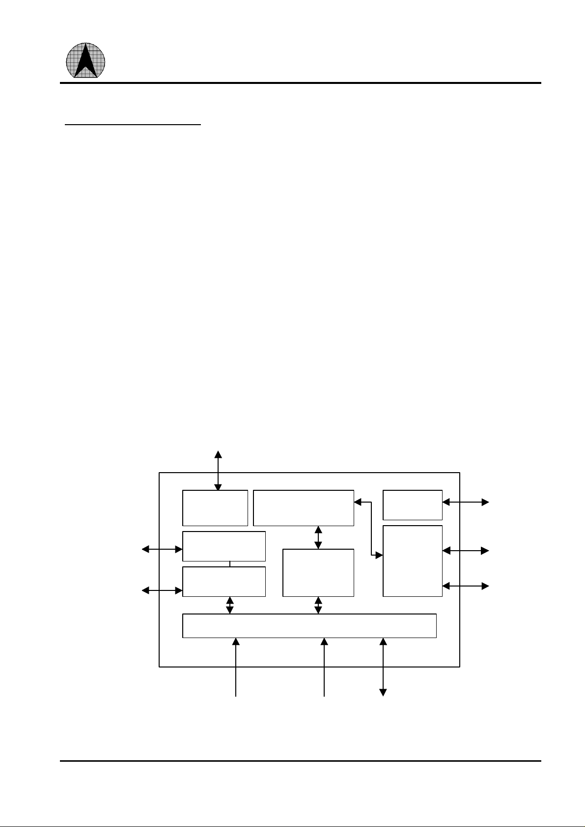
1.2 AX88190A Block Diagram:
SMDC
EECS
EECK
EEDI
GPI/O
MODEM
I/F
SEEPROM
NE2000/GPIO
8K* 16 SRAM
and Memory Arbiter
Remote
DMA
FIFOs
PCMCIA Interface
STA
MAC
Core
Fig - 1 AX88190A Block Diagram
5
ASIX ELECTRONICS CORPORATION
AX88190A PCMCIA Fast Ethernet MAC Controller
SA[1]
HVDD
HVDD
SA[0]
SA[3]
SA[2]
SA[5]
SA[4]
SA[6]
SA[7]
SA[9]
SA[8]
IREQ#
IORD#
IOWR#
SD[15]
SD[14]
SD[13]
SD[12]
SD[11]
SD[10]
SD[9]
SD[8]
SD[6]
SD[5]
SD[7]
CE2#
CE1#
GPIO1#
GPIO0#
1.3 AX88190A Pin Connection Diagram
The AX88190A is housed in the 128-pin plastic light quad flat pack. See Fig - 2 AX88190A Pin
Connection Diagram.
TXD[1]
TXD[2]
TXD[3]
LVDD
CLKO
VSS
LCLK/XTALIN
XTALOUT
VSS
EECS
EECK
EEDI
EEDO
LVDD
MDCS#
MINT
MAUDIO
PPWDN
MRIN#
MPWDN
MRESET#
MRDY
VSS
IOIS16#
STSCHG#
SPKR#
REG#
INPACK#
WAIT#
LVDD
RESET
LVDD
97
98
99
100
101
102
103
104
105
106
107
108
109
110
111
112
113
114
115
116
117
118
119
120
121
122
123
124
125
126
127
128
TX_EN
TXD[0]
TX_CLK
94
95
96
3
1
2
MDC
VSS
93
928589
MDIO
RXD[3]
RXD[2]
90
RXD[1]
88
RXD[0]
RX_CLK
CRS
86
87
COL
RX_DV
84
83
RX_ER
VSS
SCRS
829181
SRXD
SRXC
78
797480
TEST
SCOL
77
76
SLINK#
NC
HVDD
EEPROM_SIZE
75
72
73
NC
71
AX88190A
PCMCIA
10/100BASE MAC
CONTROLLER
8
7
4
6
5
9
10
11
12
13
14
15
16
17
18
19
20
21
22
23
24
25
26
VSS
STXE
70
69
28
27
NC
STXC
CLK_DIV3#
STXD
66
65
68
67
32
31
29
30
64
63
62
61
60
59
58
57
56
55
54
53
52
51
50
49
48
47
46
45
44
43
42
41
40
39
38
37
36
35
34
33
HVDD
NC
NC
GPI0
GPI1
VSS
GPI2
GPI3
NC
NC
LVDD
NC
NC
NC
NC
VSS
NC
NC
NC
LVDD
GPIO2
GPIO3
VSS
VSS
SD[0]
SD[1]
SD[2]
SD[3]
VSS
SD[4]
Fig - 2 AX88190A Pin Connection Diagram
VSS
WE#
OE#
6
VSS
ASIX ELECTRONICS CORPORATION

AX88190A PCMCIA Fast Ethernet MAC Controller
2.0 Signal Description
The following terms describe the AX88190A pin-out:
All pin names with the “#” suffix are asserted low.
The following abbreviations are used in following Tables.
I Input PU Pull Up
O Output PD Pull Down
I/O Input/Output P Power Pin
OD Open Drain
2.1 PCMCIA Bus Interface Signals Group
SIGNAL TYPE PIN NO. DESCRIPTION
SA[9:0] I 10 – 1 System Address : Signals SA[9:0] are address bus input lines which
enable direct address of up to 64K memory and I/O spaces on card.
SD[15:0] I/O 20 – 23,
25 – 38,
30 – 33,
35 – 38
IREQ# O 12 Interrupt Request : IREQ# is asserted to indicate the host system that
WAIT# O 125 Wait : This signal is set low to insert wait states during Remote DMA
REG# I 123 Attribute Memory and I/O Space Select : When the REG# signal is
IORD# I 15 I/O Read : The host asserts IORD# to read data from AX88190A I/O
IOWR# I 14 I/O Write : The host asserts IOWR# to write data into AX88190A I/O
OE# I 16 Output Enable : The OE# line is used to gate Memory Read data from
WE# I 13 Write Enable : The WE# signal is used for strobing Memory Write
IOIS16# O 120 I/O is 16 Bit Port : The IOIS16# is asserted when the address at the
INPACK# O 124 Input Port Acknowledge : The signal is asserted when the AX88190A
CE1#-CE2# I 18, 17 Card Enable : The CE1# enables even numbered address bytes and
BVD1_STSCHG# O 121 Battery Voltage Detect 1 / Status Change
BVD2_SPKR# O 122 Battery Voltage Detect 2 / Audio speaker out
System Data Bus : Signals SD[15:0] constitute the bi-directional data
bus.
the PC Card device requires host software service.
transfer.
asserted, access is limited to Attribute Memory and to the I/O space.
space.
space.
memory on PC Card
data into the memory on PC Card.
socket corresponds to an I/O address to which the card responds, and
the I/O port addressed is capable of 16-bit access.
is selected and can respond to and I/O read cycle at the address on the
address bus.
CE2# enables odd numbered address bytes
Tab - 1 PCMCIA bus interface signals group
7
ASIX ELECTRONICS CORPORATION

AX88190A PCMCIA Fast Ethernet MAC Controller
2.2 EEPROM Signals Group
SIGNAL TYPE PIN NO. DESCRIPTION
EECS O 106 EEPROM Chip Select : EEPROM chip select signal.
EECK O 107 EEPROM Clock : Signal connected to EEPROM clock pin.
EEDI O 108 EEPROM Data In : Signal connected to EEPROM data input pin.
EEDO I/PU 109 EEPROM Data Out : Signal connected to EEPROM data output pin.
Tab - 2 EEPROM bus interface signals group
2.3 MII interface signals group
SIGNAL TYPE PIN NO. DESCRIPTION
RXD[3:0] I 90 – 87 Receive Data : RXD[3:0] is driven by the PHY synchronously with
respect to RX_CLK.
CRS I 85 Carrier Sense : Asynchronous signal CRS is asserted by the PHY
when either the transmit or receive medium is non-idle.
RX_DV I 83 Receive Data Valid : RX_DV is driven by the PHY synchronously
with respect to RX_CLK. Asserted high when valid data is present on
RXD [3:0].
RX_ER I 82 Receive Error : RX_ER ,is driven by PHY and synchronous to
RX_CLK, is asserted for one or more RX_CLK periods to indicate to
the port that an error has detected.
RX_CLK I 86 Receive Clock : RX_CLK is a continuous clock that provides the
timing reference for the transfer of the RX_DV,RXD[3:0] and
RX_ER signals from the PHY to the MII port of the repeater.
COL I 84 Collision : this signal is driven by PHY when collision is detected.
TX_EN O 95 Transmit Enable : TX_EN is transition synchronously with respect to
the rising edge of TX_CLK. TX_EN indicates that the port is
presenting nibbles on TXD [3:0] for transmission.
TXD[3:0] O 99 – 96 Transmit Data : TXD[3:0] is transition synchronously with respect to
the rising edge of TX_CLK. For each TX_CLK period in which
TX_EN is asserted, TXD[3:0] are accepted for transmission by the
PHY.
TX_CLK I 94 Transmit Clock : TX_CLK is a continuous clock from PHY. It
provides the timing reference for the transfer of the TX_EN and
TXD[3:0] signals from the MII port to the PHY.
MDC O 92 Station Management Data Clock : The timing reference for MDIO.
All data transfers on MDIO are synchronized to the rising edge of this
clock. MDC is a 2.5MHz frequency clock output.
MDIO I/O/PU 91 Station Management Data Input / Output : Serial data input/output
transfers from/to the PHYs . The transfer protocol conforms to the
IEEE 802.3u MII specification.
Tab - 3 MII interface signals group
8
ASIX ELECTRONICS CORPORATION

AX88190A PCMCIA Fast Ethernet MAC Controller
2.4 SNI Interface pins group
SIGNAL TYPE PIN NO. DESCRIPTION
STXC I 66 Transmit Clock : this signal is driven by PHY with 20MHz clock.
STXD O 68 Transmit Data : STXD is transition synchronously with respect to the
rising edge of STXC. For each STXC period in which STXE is
asserted, STXD is accepted for transmission by the PHY.
STXE O 70 Transmit Enable : STXE is transition synchronously with respect to
the rising edge of STXC. STXE indicates that the port is presenting
data on STXD for transmission.
SCOL I 76 Collision : this signal is driven by PHY when collision is detected.
SRXC I 78 Receive Clock : SRXC is driven by PHY for received data
synchronization.
SRXD I 79 Receive Data : SRXD is driven by the PHY synchronously with respect
to SRXC.
SCRS I 80 Carrier Sense : Asynchronous signal SCRS is asserted by the PHY
when either the transmit or receive medium is non-idle.
SLINK# I/PU 74 Link indicator : Active low indicate the SNI interface is link to
network. When SNI is not used must keep the pin no connection or
pull high the signal.
Tab - 4 Serial Network Interface pins group
2.5 Modem interface pins group
Signal Name Type Pin No. Description
MRDY I/PU 118 Modem Ready : MRDY low indicates that modem is initializing the
modem after reset signal asserted or the modem is at SLEEP/STOP
mode.
MRESET# O 117 Modem Reset :This signal asserts low to reset the modem chipset.
MDCS# O 111 Modem Chip Select : This signal connected to modem chip select pin.
MPWDN O 116 Modem Power Down : Rockwell modem chipset, this signal asserts
low to let modem chipset into power down mode. AT&T modem
chipset, this signal asserts high to let modem chipset into power down
mode.
MINT I/PD 112 Modem Interrupt : This signal driven by modem chipset to active
interrupt.
MRIN# I/PU 115 Ring Input :This signal is driven by DAA’s ring detect circuit. When
a telephone ringing signal is being received.
MAUDIO I/PD 113 Modem Audio : This signal is passed to PCMCIA interface via SPKR.
Tab - 5 Modem interface signals group
2.6 General Purpose I/O pins group
Signal Name Type Pin No. Description
GPI[3] I 57 Read register offset 18h bit 3 value reflects this input value.
GPI[2] I 58 Read register offset 18h bit 2 value reflects this input value.
GPI[1] I 60 Read register offset 18h bit 1 value reflects this input value.
GPI[0] I 61 Read register offset 18h bit 0 value reflects this input value.
9
ASIX ELECTRONICS CORPORATION

AX88190A PCMCIA Fast Ethernet MAC Controller
GPIO3# I/O 41 Default “1”. The pin reflects register offset 1Ah bit 3 inverted value.
GPIO2 I/O 42 Default “0”. The pin reflects register offset 1Ah bit 2 value.
GPIO1# I/O 43 Default “1”. The pin reflects register offset 1Ah bit 1 inverted value.
GPIO0# I/O 45 Default “1”. The pin reflects register offset 1Ah bit 0 inverted value.
Tab - 6 General Pursose I/O pins group
2.7 Miscellaneous pins group
SIGNAL TYPE PIN NO. DESCRIPTION
LCLK/XTALIN I 103 CMOS Local Clock : Typical a 25Mhz clock, +/- 100 ppm, 40%-60%
duty cycle. ( See application note also )
Crystal Oscillator Input : Typical a 25Mhz crystal, +/- 25 ppm can be
connected across XTALIN and XTALOUT.
XTALOUT O 104 Crystal Oscillator Output : Typical a 25Mhz crystal, +/- 25 ppm can be
connected across XTALIN and XTALOUT. If a single-ended external
clock (LCLK) is connected to XTALIN, the crystal output pin should
be left floating.
CLKO O 101 Clock Output : This clock is source from LCLK/XTALIN.
CLK_DIV3# I/PU 67 Clock Devide 3 Enable : Active low to enable the devided 3 circuit.
That internally devides LCLK/XTALIN input frequeny by 3 and then
feed into internal circuit for system clock used.
Default value set to logic high, this function is disabled.
PPWDN O 114 Phy Power Down : This pin connects to PHY chip power down mode
control input.
RESET I/PD 127 Reset
Reset is active high then place AX88190A into reset mode
immediately. During Falling edge the AX88190A loads the EEPROM
data.
TEST# I/PU 77
EEPROM SIZE I/PU 73 EEPROM SIZE = 0 : 93C46 128 byte type EEPROM is used.
NC N/A 46–48, 50–
53, 55-56,
LVDD P 44, 54,
100, 110,
126, 128
HVDD P 19, 29, 64,75Power Supply : +5V DC.
VSS P 11, 24, 34,
39, 40, 49,
59, 69, 81,
93, 102, 105,
119
Test Pin : Active LOW
The pin is just for test mode setting purpose only. Must be pull high
when normal operation.
EEPROM SIZE = 1 : 93C56 256 byte type EEPROM is used.
No Connection : for manufacturing test only.
Power Supply : +3.3V DC.
Note : for pure 3.3V single power solution, all the HVDD pin can
connect to +3.3V. Care should be taken that HVDD input power must
be greater or equal ( > = ) than LVDD.
Power Supply : +0V DC or Ground Power.
Tab - 7 Miscellaneous pins group
10
ASIX ELECTRONICS CORPORATION

AX88190A PCMCIA Fast Ethernet MAC Controller
2.8 Power on configuration setup signals cross reference table
Signal Name Share with Description
MPD_SET STXD MPD_SET = 0 : MPWDN pin active high.
MPD_SET = 1 : MPWDN pin active low.
PPD_SET STXE PPD_SET = 0 : PPWDN pin active high.
PPD_SET = 1 : PPWDN pin active low.
All of the above signals are pull-up for default values.
Tab - 8 Power on Configuration Setup Table
11
ASIX ELECTRONICS CORPORATION

AX88190A PCMCIA Fast Ethernet MAC Controller
3.0 Memory and I/O Mapping
There are four memory or I/O mapping used in AX88190A.
1. EEPROM Memory Mapping
2. Attribute Memory Mapping
3. I/O Mapping
4. Local Memory Mapping
3.1 EEPROM Memory Mapping
EEPROM OFFSET HIGH BYTE LOW BYTE
00H RESERVED WORD COUNT
01H CFH CFL
02H NODE-ID1 NODE ID 0
03H NODE ID 3 NODE ID 2
04H NODE ID 5 NODE ID 4
05H CHECKSUM RESERVED
06H – 10H RESERVED RESERVED
10H – FFH CIS CIS
Tab - 9 EEPROM Memory Mapping
Note : bit 3 register of LCOR in AX88190 is replaced by bit 0 of CFL in AX88190A
Bit 0 of CFL : Enable Power Down mode
this bit is set to 1, the LAN will go into power down mode. At power down mode AX88190A will disable MAC
transmitting and receiving operation. But the host interface will not be affected.
3.2 Attribute Memory Mapping
ATTRIBUTE MEMORY
OFFSET
0000H
03BFH
03C0H LCOR
03C2H LCCSR
03C4H 03C6H -
03CAH LIOBASE0
03CCH LIOBASE1
03CEH
03DFH
03E0H MCOR
03E2H MCCSR
03E4H 03E6H -
03EAH MIOBASE0
03ECH MIOBASE1
03EEH
03FFH
CONTENTS
CIS
RESERVED
RESERVED
Tab - 10 Attribute Memory Mapping
12
ASIX ELECTRONICS CORPORATION

AX88190A PCMCIA Fast Ethernet MAC Controller
3.3 I/O Mapping
SYSTEM I/O OFFSET FUNCTION
0000H
001FH
Tab - 11 I/O Address Mapping
3.4 SRAM Memory Mapping
OFFSET FUNCTION
0000H
03BFH
03C0H LCOR *1
03C2H LCCSR *1
03C4H 03C6H -
03CAH LIOBASE0 *1
03CCH LIOBASE1 *1
03CEH
03DFH
03E0H MCOR *1
03E2H MCCSR *1
03E4H 03E6H -
03EAH MIOBASE0 *1
03ECH MIOBASE1 *1
03EEH
03FFH
0400H NODE ID 0
0401H NODE ID 1
0402H NODE ID 2
0403H NODE ID 3
0404H NODE ID 4
0405H NODE ID 5
0406H
07FFH
4000H
7FFFH
MAC CORE REGISTER
CIS *1
RESERVED
RESERVED
RESERVED
8K X 16
SRAM BUFFER
Tab - 12 Local Memory Mapping
13
ASIX ELECTRONICS CORPORATION

AX88190A PCMCIA Fast Ethernet MAC Controller
4.0 Registers Operation
There are three register sets in AX88190A :
The PCMCIA function configuration registers of LAN.
The PCMCIA function configuration registers of MODEM.
The MAC core register.
4.1 PCMCIA Function Configuration Register Set of LAN
REGISTER NAME OFFSET
LCOR CONFIGURATION OPTION REGISTER 3C0H
LCSR CONFIGURATION AND STATUS REGISTER 3C2H
LIOBASE0 I/O BASED REGISTER 0 3CAH
LIOBASE1 I/O BASED REGISTER 1 3CCH
Tab - 13 PCMCIA Function Configuration Register Mapping of LAN
14
ASIX ELECTRONICS CORPORATION

AX88190A PCMCIA Fast Ethernet MAC Controller
4.1.1 Configuration Option Register of LAN (LCOR) Offset 3C0H (Read/Write)
FIELD R/W/C DESCRIPTION
7 R/W Software Reset
Assert this bit will reset the LAN function of AX88190A. Return a 0 to this bit will leave
the LAN function of AX88190A in a post-reset state as same as that following a hardware
reset. The value of this bit is 0 at power-on.
6 R/W Level IRQ
This bit should be set to 1, the AX88190A always generates Level Mode Interrupt.
5:0 R/W Function Configuration Index
These six bits are used to indicate entry of the card configuration table locate in the CIS.
The default value is 0
.
On multifunction PC Card,
Bit 5, Bit 4, Bit 3 : MODEM I/O base registers
Bit 5 Bit 4 Bit 3 LAN I/O base MODEM I/O base
0 0 0 300H Decided by MIOBASE registers
0 0 1 320H 2f8H
0 1 0 340H 3e8H
0 1 1 360H 2e8H
1 0 0 380H Decided by MIOBASE registers
1 0 1 200H 2f8H
1 1 0 220H 3e8H
1 1 1 240H 2e8H
Bit 2 : Enable IREQ# Routing
If bit 0 of LCOR is set to 0, this bit is ignored.
If bit 0 of LCOR is set to 1 and this bit is set to 1, the LAN will generate interrupt request
via IREQ# signal. If this bit is set to 0, the LAN will not generate interrupt request via
IREQ# line.
Bit 1 : Enable Base and Limit Registers
If bit 0 of LCOR is set to 0, this bit is ignored.
If bit 0 of LCOR is set to 1 and this bit is set to 1,only I/O addresses that are qualified by
the Base and Limit registers are passed to LAN function. If this bit is set to 0,all I/O
addresses are passed to LAN function.
Bit 0 : Enable Function
If this bit is set to 0, the LAN function is disabled.
If this bit is set to 1, the LAN function is enabled.
15
ASIX ELECTRONICS CORPORATION
 Loading...