

Page 1

LCD
LCD
LCD
LCD TV
TV
TV
TV
SERVICE
SERVICE
SERVICE
SERVICE MANUAL
CHASSIS : AS-MST6M182VG-LE2
MODEL :LED2295
CAUTION
BEFORE SERVICING THE CHASSIS,
READ THE SAFETY PRECAUTIONS IN THIS MANUAL.
MANUAL
MANUAL
MANUAL
Page 2

CONTENTS
C ontents .............................................................................................. 2
P roduct safety .................................................................................. 3
S pecification ........................................................................................ 7
Software upgrade ........................................................................................ 10
S vc.sheet ............................................................................................... 17
Page 3

SAFETY
SAFETY
SAFETY
SAFETY PRECAUTIONS
PRECAUTIONS
PRECAUTIONS
PRECAUTIONS
IMPORTANT
IMPORTANT
IMPORTANT
IMPORTANT SAFETY
Many electrical and mechanical parts in this chassis have special safety-related characteristics. These parts are identified by
in the Schematic Diagram and Replacement Parts List.
It is essential that these special safety parts should be replaced with the same components as recommended in this manual to
prevent Shock, Fire, or other Hazards.
Do not modify the original design without permission of manufacturer.
General
General
General
General Guidance
AC power line. Use a transformer of adequate power rating as this protects the technician from accidents resulting in personal
injury from electrical shocks.
inadvertently introduced during the service operation.
If any fuse (or Fusible Resistor) in this TV receiver is blown,replace it with the specified.
Before returning the receiver to the customer, always perform an AC leakage current check on the exposed metallic parts of the
cabinet, such as antennas, terminals, etc., to be sure the set is safe to operate without damage of electrical shock.
Guidance
Guidance
Guidance
An isolation Transformer should always be used during the servicing of a receiver whose chassis is not isolated from the
It will also protect the receiver and it's components from being damaged by accidental shorts of the circuitry that may be
When replacing a high wattage resistor (Oxide Metal Film Resistor, over 1W), keep the resistor 10mm away from PCB.
Keep wires away from high voltage or high temperature parts.
SAFETY
SAFETY
SAFETY NOTICE
NOTICE
NOTICE
NOTICE
Leakage
Leakage
Leakage
Leakage Current
With the instrument AC plug removed from AC source, connect an electrical jumper across the two AC plug prongs. Place the
AC switch in the on position, connect one lead of ohm-meter to the AC plug prongs tied together and touch other ohm-meter lead
in turn to each exposed metallic parts such as antenna terminals, phone jacks, etc.
If the exposed metallic part has a return path to the chassis, the measured resistance should be between 1M Ω and 5.2M Ω .
When the exposed metal has no return path to the chassis the reading must be infinite.
An other abnormality exists that must be corrected before the receiver is returned to the customer.
Leakage
Leakage
Plug the AC cord directly into the AC outlet.
capacitor between a known good earth ground (Water Pipe, Conduit, etc.) and the exposed metallic parts.
voltage measured must not exceed 0.75 volt RMS which is corresponds to 0.5mA.
In case any measurement is out of the limits specified, there is possibility of shock hazard and the set must be checked and
repaired before it is returned to the customer.
Current
Current
Current Cold
Leakage
Leakage Current
Do not use a line Isolation Transformer during this check. Connect 1.5K/10watt resistor in parallel with a 0.15uF
Measure the AC voltage across the resistor using AC voltmeter with 1000 ohms/volt or more sensitivity.
Reverse plug the AC cord into the AC outlet and repeat AC voltage measurements for each exposed metallic part. Any
Cold
Cold
Cold Check(Antenna
Current
Current
Current Hot
Hot
Hot
Hot Check
Check(Antenna
Check(Antenna
Check(Antenna Cold
Check
Check
Check (See
(See
(See
(See below
Cold
Cold
Cold Check
below
below
below Figure)
Check
Check
Check
Figure)
Figure)
Figure)
Page 4
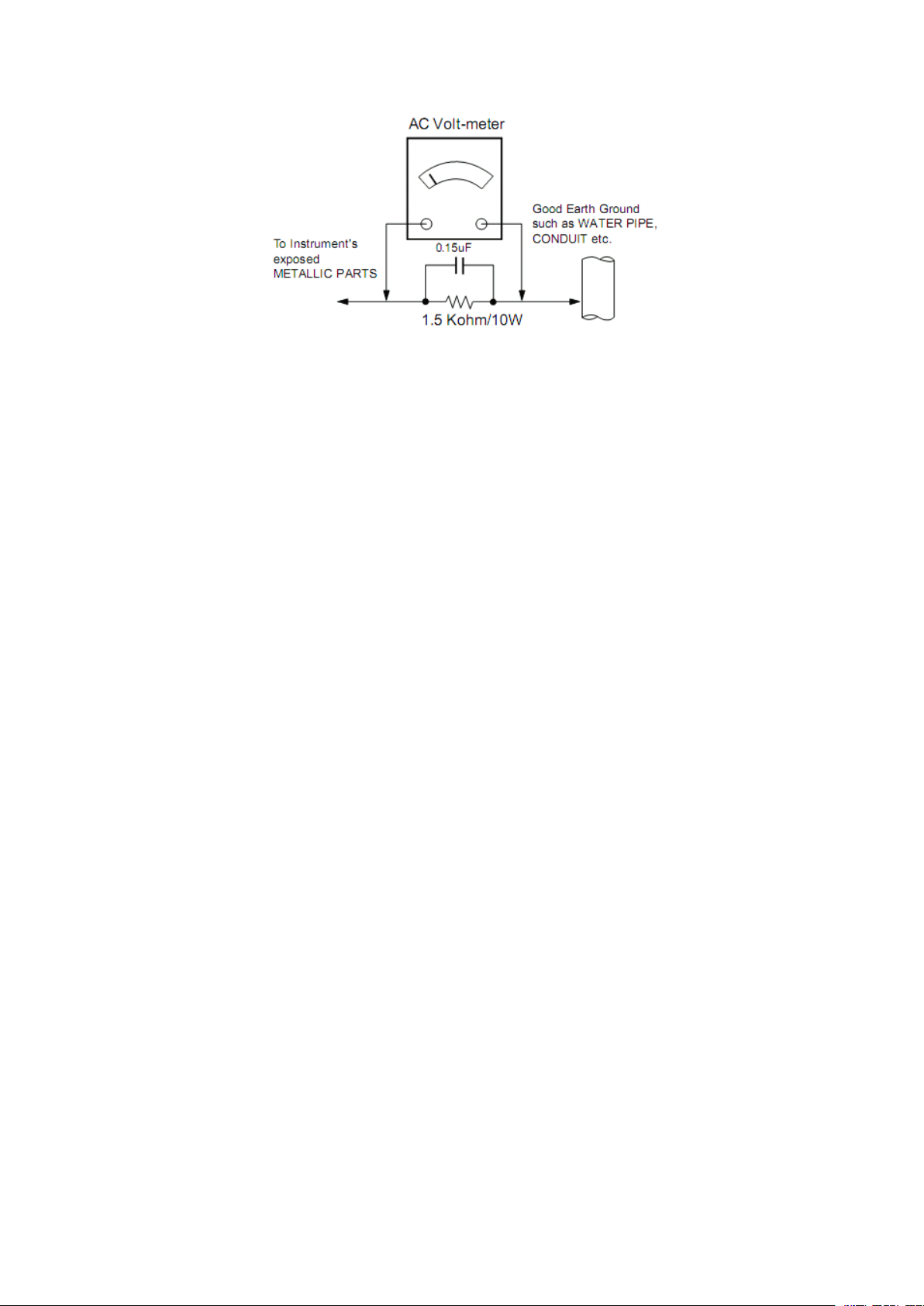
Leakage
Leakage
Leakage
Leakage Current
Current
Current
Current Hot
Hot
Check
Hot
Check
Hot Check
Check circuit
circuit
circuit
circuit
SERVICING
SERVICING
SERVICING
SERVICING PRECAUTIONS
CAUTION
CAUTION
CAUTION
CAUTION : Before servicing receivers covered by this service manual and its supplements and addenda, read and follow
SAFETY PRECAUTIONS on page 3 of this publication.
NOTE:
NOTE:
NOTE:
NOTE: If unforeseen circumstances create conflict between the following servicing precautions and any of the safety
precautions on page 3 of this publication, always follow the safety precautions. Remember: Safety First.
General
General
General
General Servicing
1. Always unplug the receiver AC power cord from the AC power source before;
a. Removing or reinstalling any component, circuit board module or any other receiver assembly.
b. Disconnecting or reconnecting any receiver electrical plug or other electrical connection.
c. Connecting a test substitute in parallel with an electrolytic capacitor in the receiver.
CAUTION
CAUTION
CAUTION
CAUTION : A wrong part substitution or incorrect polarity installation of electrolytic capacitors may result in an
explosion hazard.
2. Test high voltage only by measuring it with an appropriate high voltage meter or other voltage measuring device (DVM,
FETVOM , etc) equipped with a suitable high voltage probe. Do not test high voltage by "drawing an arc".
3. Do not spray chemicals on or near this receiver or any of its assemblies.
4. Unless specified otherwise in this service manual, clean electrical contacts only by applying the following mixture to the
contacts with a pipe cleaner, cotton-tipped stick or comparable non-abrasive applicator; 10% (by volume) Acetone and 90%
(by volume) isopropyl alcohol (90%-99% strength)
CAUTION
CAUTION
CAUTION
CAUTION : This is a flammable mixture.
Unless specified otherwise in this service manual, lubrication of contacts in not required.
5. Do not defeat any plug/socket B+ voltage interlocks with which receivers covered by this service manual might be
equipped.
6. Do not apply AC power to this instrument and/or any of its electrical assemblies unless all solid-state device heat sinks ar
correctly installed.
7. Always connect the test receiver ground lead to the receiver chassis ground before connecting the test receiver positive
lead.
Always remove the test receiver ground lead last.
8. Use with this receiver only the test fixtures specified in this service manual.
CAUTION:
CAUTION:
CAUTION:
CAUTION: Do not connect the test fixture ground strap to any heat sink in this receiver.
Servicing
Servicing
Servicing Precautions
Precautions
Precautions
Precautions
PRECAUTIONS
PRECAUTIONS
PRECAUTIONS
Electrostatically Sensitive (ES) Devices
Some semiconductor (solid-state) devices can be damaged easily by static electricity. Such components commonly are called
Electrostatically Sensitive (ES) Devices. Examples of typical ES devices are integrated circuits and some field-effect
transistors and semiconductor "chip" components. The following techniques should be used to help reduce the incidence of
component damage caused by static by static electricity.
Page 5

1. Immediately before handling any semiconductor component or semiconductor-equipped assembly, drain off any
electrostatic charge on your body by touching a known earth ground. Alternatively, obtain and wear a commercially available
discharging wrist strap device, which should be removed to prevent potential shock reasons prior to applying power to the unit
under test.
2. After removing an electrical assembly equipped with ES devices, place the assembly on a conductive surface such as
aluminum foil, to prevent electrostatic charge buildup or exposure of the assembly
3. Use only a grounded-tip soldering iron to solder or unsolder ES devices.
4. Use only an anti-static type solder removal device. Some solder removal devices not classified as "anti-static" can
generate electrical charges sufficient to damage ES devices.
5. Do not use freon-propelled chemicals. These can generate electrical charges sufficient to damage ES devices.
6. Do not remove a replacement ES device from its protective package until immediately before you are ready to install it.
(Most replacement ES devices are packaged with leads electrically shorted together by conductive foam, aluminum foil or
comparable conductive material).
7. Immediately before removing the protective material from the leads of a replacement ES device, touch the protective
material to the chassis or circuit assembly into which the device will be installed.
CAUTION
CAUTION
CAUTION
CAUTION : Be sure no power is applied to the chassis or circuit, and observe all other safety precautions.
8. Minimize bodily motions when handling unpackaged replacement ES devices. (Otherwise harmless motion such as the
brushing together of your clothes fabric or the lifting of your foot from a carpeted floor can generate static electricity sufficient
to damage an ES device.)
General
General
General
General Soldering
1. Use a grounded-tip, low-wattage soldering iron and appropriate tip size and shape that will maintain tip temperature within
the range or 500 ° F to 600 °
2. Use an appropriate gauge of RMA resin-core solder composed of 60 parts tin/40 parts lead.
3. Keep the soldering iron tip clean and well tinned.
4. Thoroughly clean the surfaces to be soldered. Use a mall wire-bristle (0.5 inch, or 1.25cm) brush with a metal handle.
Do not use freon-propelled spray-on cleaners.
5. Use the following unsoldering technique
a. Allow the soldering iron tip to reach normal temperature. (500 ° F to 600 ° F)
b. Heat the component lead until the solder melts.
c. Quickly draw the melted solder with an anti-static, suction-type solder removal device or with solder braid.
CAUTION
CAUTION
CAUTION
CAUTION : Work quickly to avoid overheating the circuit board printed foil.
6. Use the following soldering technique.
a. Allow the soldering iron tip to reach a normal temperature (500 ° F to 600 ° F)
b. First, hold the soldering iron tip and solder the strand against the component lead until the solder melts.
c. Quickly move the soldering iron tip to the junction of the component lead and the printed circuit foil, and hold it there only
until the solder flows onto and around both the component lead and the foil.
CAUTION
CAUTION
CAUTION
CAUTION : Work quickly to avoid overheating the circuit board printed foil.
d. Closely inspect the solder area and remove any excess or splashed solder with a small wire-bristle brush.
Soldering
Soldering
Soldering Guidelines
Guidelines
Guidelines
Guidelines
F.
IC
Remove/Replacement
IC
Remove/Replacement
IC
IC Remove/Replacement
Remove/Replacement
Some chassis circuit boards have slotted holes (oblong) through which the IC leads are inserted and then bent flat against the
circuit foil. When holes are the slotted type, the following technique should be used to remove and replace the IC. When working
with boards using the familiar round hole, use the standard technique as outlined in paragraphs 5 and 6 above.
Removal
Removal
Removal
Removal
1. Desolder and straighten each IC lead in one operation by gently prying up on the lead with the soldering iron tip as the solder
melts.
2. Draw away the melted solder with an anti-static suction-type solder removal device (or with solder braid) before removing the
IC.
Page 6

Replacement
Replacement
Replacement
Replacement
1. Carefully insert the replacement IC in the circuit board.
2. Carefully bend each IC lead against the circuit foil pad and solder it.
3. Clean the soldered areas with a small wire-bristle brush. (It is not necessary to reapply acrylic coating to the areas).
"Small-Signal" Discrete Transistor
Removal/Replacement
Removal/Replacement
Removal/Replacement
Removal/Replacement
1. Remove the defective transistor by clipping its leads as close as possible to the component body.
2. Bend into a "U" shape the end of each of three leads remaining on the circuit board.
3. Bend into a "U" shape the replacement transistor leads.
4. Connect the replacement transistor leads to the corresponding leads extending from the circuit board and crimp the "U" with
long nose pliers to insure metal to metal contact then solder each connection.
Power
Power
Power
Power Output,
Removal/Replacement
Removal/Replacement
Removal/Replacement
Removal/Replacement
1. Heat and remove all solder from around the transistor leads.
2. Remove the heat sink mounting screw (if so equipped).
3. Carefully remove the transistor from the heat sink of the circuit board.
4. Insert new transistor in the circuit board.
5. Solder each transistor lead, and clip off excess lead.
6. Replace heat sink.
Diode
Diode
Diode
Diode Removal/Replacement
1. Remove defective diode by clipping its leads as close as possible to diode body.
2. Bend the two remaining leads perpendicular y to the circuit board.
3. Observing diode polarity, wrap each lead of the new diode around the corresponding lead on the circuit board.
4. Securely crimp each connection and solder it.
5. Inspect (on the circuit board copper side) the solder joints of the two "original" leads. If they are not shiny, reheat them and if
necessary, apply additional solder.
Fuse
Fuse
Fuse
Fuse and
Removal/Replacement
Removal/Replacement
Removal/Replacement
Removal/Replacement
1. Clip each fuse or resistor lead at top of the circuit board hollow stake.
2. Securely crimp the leads of replacement component around notch at stake top.
3. Solder the connections.
CAUTION:
CAUTION:
CAUTION:
CAUTION: Maintain original spacing between the replaced component and adjacent components and the circuit board to
prevent excessive component temperatures.
Output,
Output,
Output, T ransistor
Removal/Replacement
Removal/Replacement
Removal/Replacement
and
and
and Conventional
Transistor
Transistor
Transistor Device
Conventional
Conventional
Conventional Resistor
Device
Device
Device
Resistor
Resistor
Resistor
Circuit
Circuit
Circuit
Circuit Board
Excessive heat applied to the copper foil of any printed circuit board will weaken the adhesive that bonds the foil to the circuit
board causing the foil to separate from or "lift-off" the board. The following guidelines and procedures should be followed
whenever this condition is encountered.
At
At
At
At IC
To repair a defective copper pattern at IC connections use the following procedure to install a jumper wire on the copper pattern
side of the circuit board. (Use this technique only on IC connections).
1. Carefully remove the damaged copper pattern with a sharp knife. (Remove only as much copper as absolutely necessary).
2. carefully scratch away the solder resist and acrylic coating (if used) from the end of the remaining copper pattern.
3. Bend a small "U" in one end of a small gauge jumper wire and carefully crimp it around the IC pin. Solder the IC connection.
4. Route the jumper wire along the path of the out-away copper pattern and let it overlap the previously scraped end of the good
Board
Board
Board Foil
IC
Connections
IC
Connections
IC Connections
Connections
Foil
Foil
Foil Repair
Repair
Repair
Repair
Page 7
copper pattern. Solder the overlapped area and clip off any excess jumper wire.
At
Other
At
At
At Other
Use the following technique to repair the defective copper patternat connections other than IC Pins. This technique involves the
nstallation of a jumper wire on the component side of the circuit board.
1. Remove the defective copper pattern with a sharp knife. Remove at least 1/4 inch of copper, to ensure that a hazardous
condition will not exist if the jumper wire opens.
2. Trace along the copper pattern from both sides of the pattern break and locate the nearest component that is directly
connected to the affected copper pattern.
3. Connect insulated 20-gauge jumper wire from the lead of the nearest component on one side of the pattern break to the lead
of the nearest component on the other side. Carefully crimp and solder the connections.
CAUTION
CAUTION
CAUTION
CAUTION : Be sure the insulated jumper wire is dressed so the it does not touch components or sharp edges.
NOTE
NOTE
NOTE
NOTE : Specifications and others are subject to change without notice for improvement.
1. Application range
This specification is applied to the LED TV used AS-MST6M182VG-LE2 chassis.
2. Requirement for Test
Each part is tested as below without special appointment.
1) Temperature : 25 ± 5 º C (77 ± 9 º F), CST : 40 ± 5 º C
2) Relative Humidity : 65 ± 10%
3) Power Voltage : Standard input voltage(100-240V~, 50/60Hz)
* Standard Voltage of each products is marked by models.
4) Specification and performance of each parts are followed each drawing and specification by part number in accordance with
BOM.
5) The receiver must be operated for about 20 minutes prior to the adjustment.
3. Test method
1) Performance: LGE TV test method followed
2) Demanded other specification
- Safety: CB specification
- EMC: CISPR 13 specification
4.
4.
4.
4. General
Connections
Other
Connections
Other Connections
Connections
General
General
General specification
specification
specification
specification
SPECIFICATION
SPECIFICATION
SPECIFICATION
SPECIFICATION
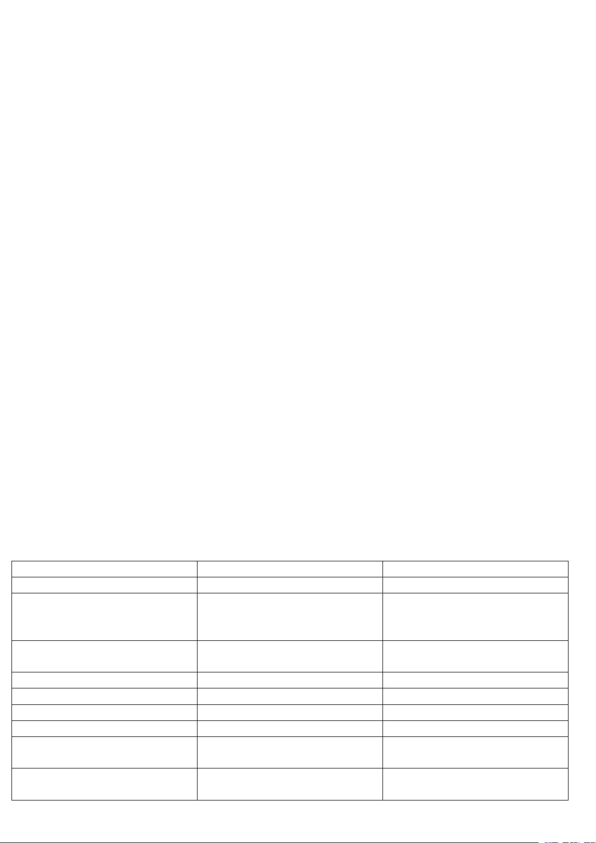
Item Specification Remark
Broadcasting system PAL-BG
1) VHF : 00 ~ 12
Available Channel
Tuner IF
Input Voltage 100 - 240V~, 50/60Hz Mark : 240V, 50Hz
Screen Size 21.6 inch Wide (1366 x 768) LC216EXN-SCA1
Aspect Ratio 16:9
Module LC216EXN-SCA1 LC216EXN-SCA1
Operating Environment
Storage Environment
2) UHF : 20 ~ 75
3) CATV : 02 ~ 44
1)
PAL
: 38.90MHz(Picture)
34.40MHz(Sound)
1) Temp : 0 ~ 40 deg
2) Humidity : ~ 80 %
1) Temp : -20 ~ 60 deg
2) Humidity : ~ 85 %
LGE Spec
Page 8
5.
Chrominance
5.
Chrominance
5.
5. Chrominance
Chrominance &
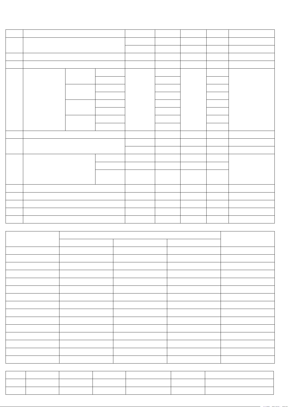
No Item Min Typ Max Unit Remark
1
White peak brightness
2 Contrast ratio cd/m2 N/A
3 Brightness uniformity 72 % Full white
4 Color coordinate
5 Color coordinate uniformity N/A
6 Contrast ratio
7 Color Temperature
8 Color Distortion, DG 10.0 %
9 Color Distortion, DP 10.0 deg
10 Color S/N, AM/FM 43 dB
11 Color Killer Sensitivity -80 dBm
&
Luminance
&
Luminance
& Luminance
Luminance Specification
RED
GREEN
BLUE
WHITE
Specification
Specification
Specification
200 250 cd/m2 LC216EXN-SCA1
X
Y 0.344
X 0.338
Y 0.618
X 0.152
Y 0.045
X 0.279
Y 0.292
Cool 8500 <Test Condition>
Medium 7500
Warm 6000
Typ..
-0.03
0.622
Typ..
+0.03
1000 LC216EXN-SCA1
LC216EXN-SCA1
HDMI input,
85% Full white
pattern
6.
Component
6.
Component
6.
6. Component
Component Video
7.
RGB
7.
RGB
7.
7. RGB
RGB PC
No Resolution H-freq(kHz) V-freq.(Hz) Pixel clock(MHz) Proposed Remark
1 720*400 31.468 70.08 28.321
2 640*480 31.469 59.94 25.17 VESA Input 848*480 60Hz,
Video
Input
(Y,
PB,
Video
Input
Input
(Y,
(Y,
(Y,
Video Input
No
1 720x480 15.73 59.94 SDTV ,DVD 480i
2 720x480 15.75 60 SDTV, DVD 480i
3 720x480 31.47 59.94 SDTV 480p
4 720X480 31.5 60 SDTV 480p
5 720x576 15.625 50 SDTV, DVD 576i
6 720x576 31.25 50 SDTV 576p
7 1280x720 44.96 59.94 HDTV 720p
8 1280x720 45 60.36 HDTV 720p
9 1280x720 37.5 50 HDTV 720p
10 1920x1080 28.125 50 HDTV 1080i
11 1920x1080 33.75 60 HDTV 1080i
12 1920x1080 33.72 59.94 HDTV 1080i
13 1920x1080 56.25 50 HDTV 1080p
14 1920x1080 67.433 59.94 HDTV 1080p
15 1920x1080 67.5 60 HDTV 1080p
PC
INPUT
PC
INPUT
PC INPUT
INPUT Mode
Mode
Mode
Mode
PR)
PB,
PR)
PB,
PB, PR)
PR)
Specification
Resolution H-freq(kHz) V-freq(Hz)
Remark
Page 9
852*480 37.684 75.00 31.50 --> 640*480 60Hz Display
3
4 1024*768
5 1280*768 47.78 59.87 79.5 WXGA
6 1360*768 47.72 59.8 84.75 WXGA
7 1366*768 47.56 59.6 84.75 WXGA
8.
HDMI
8.
HDMI
8.
8. HDMI
HDMI Input
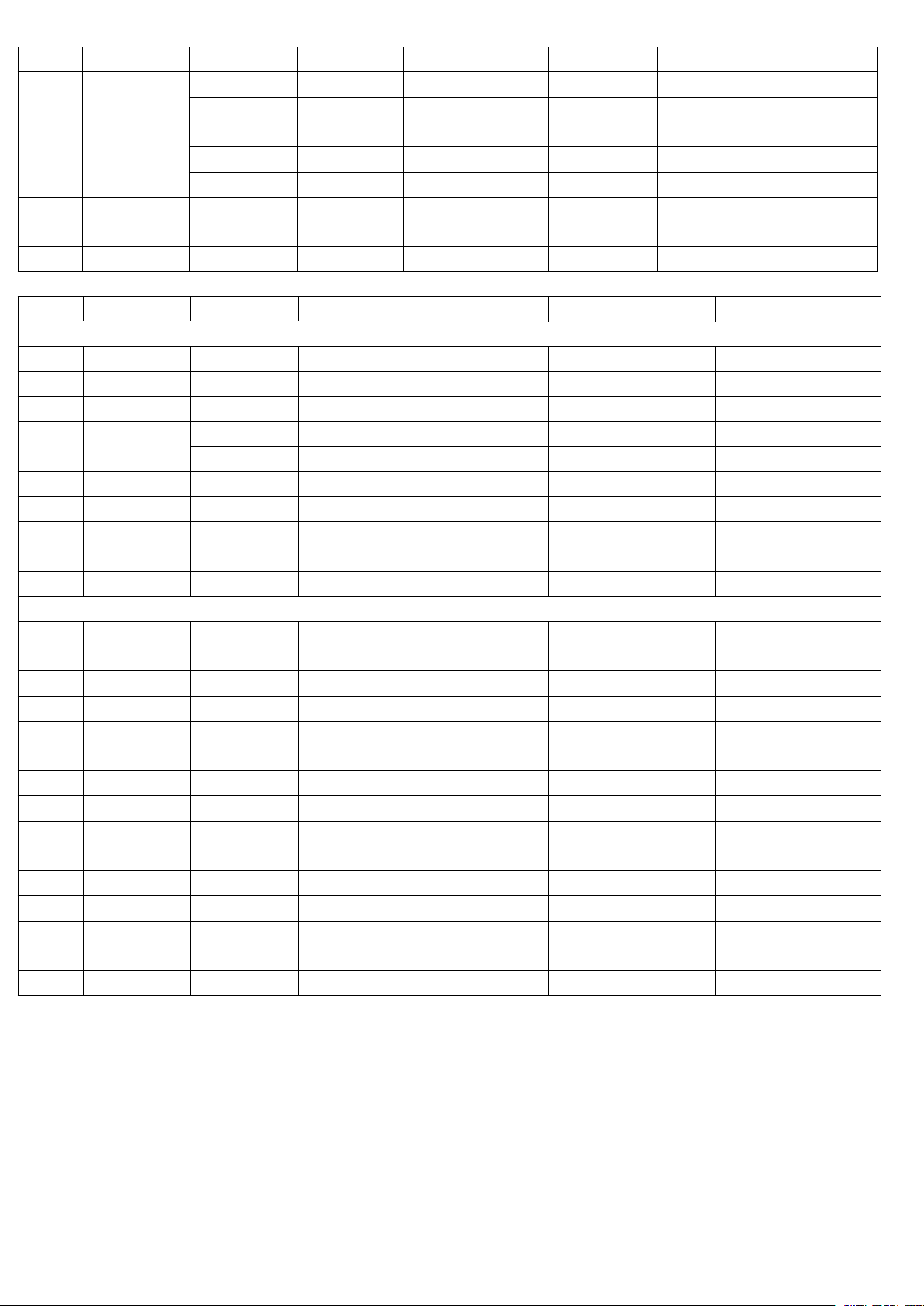
No Resolution H-freq(kHz) V -freq.(Hz) Pixel clock(MHz) Proposed Remark
PC
PC
PC
PC
1 720*400 31.468 70.08 28.321 HDCP
2 640*480 31.469 59.94 25.17 VESA HDCP
3 800*600 37.879 60.31 40.00 VESA HDCP
4 1024*768
5 1280*768 47.78 59.87 79.5 WXGA HDCP
6 1360*768 47.72 59.8 84.75 WXGA HDCP
7 1366*768 47.56 59.6 84.75 WXGA HDCP
8 1280*1024 63.595 60.0 108.875 SXGA
9 1920*1080 66.647 59.988 138.625 WUXGA
DTV
DTV
DTV
DTV
10 720*480 31.47 59.94 27.00 SDTV 480P(4:3)
11 720*480 31.50 60 27.027 SDTV 480P(4:3)
12 720*480 31.47 59.94 27.000 SDTV 480P(16:9)
13 720*480 31.50 60.00 27.027 SDTV 480P(16:9)
14 720*576 31.25 50.00 27.000 SDTV 576P
15 1280*720 37.50 50.00 74.176 HDTV 720P HDCP
16 1280*720 44.96 59.94 74.176 HDTV 720P HDCP
17 1280*720 45.00 60.00 74.250 HDTV 720P
18 1920*1080 33.72 59.94 74.176 HDTV 1080I HDCP
19 1920*1080 33.75 60.00 74.250 HDTV 1080I HDCP
20 1920*1080 28.125 50.00 74.250 HDTV 1080I 50Hz HDCP
21 1920*1080 27.000 24.00 74.250 HDTV 1080P 24Hz HDCP
22 1920*1080 56.250 50 148.500 HDTV 1080P 50Hz HDCP
23 1920*1080 67.433 59.94 148.352 HDTV 1080P HDCP
24 1920*1080 67.500 60 148.500 HDTV 1080P HDCP
800*600
Input
(PC/DTV)
Input
(PC/DTV)
Input (PC/DTV)
(PC/DTV)
37.879 60.31 40.00 VESA
46.875 75.00 49.50
48.363 60.00 65.00 VESA(XGA)
56.470 70.00 75.00
60.123 75.029 78.75
48.363 60.00 65.00 VESA(XGA) HDCP
56.470 70.00 75.00
Software
Software
Software
Software upgrade
1.
Application
1.
Application
1.
1. Application
Application Range
This specification sheet is applied to all of the LCD TV with AS-MST6M182VG-LE2 chassis.
2.
Designation
2.
Designation
2.
2. Designation
Designation
1) The adjustment is according to the order which is designated and which must be followed, according to the plan which can be
changed only on agreeing.
2) Power Adjustment: Free V oltage
Range
Range
Range
upgrade
upgrade
upgrade
Page 10
3) Magnetic Field Condition: Nil.
4) Input signal Unit: Product Specification Standard
5) Reserve after operation: Above 5 Minutes (Heat Run)
Temperature : at 25 ± 5 º C
Relative humidity : 65 ± 10%
Input voltage : 220V , 60Hz
* Download
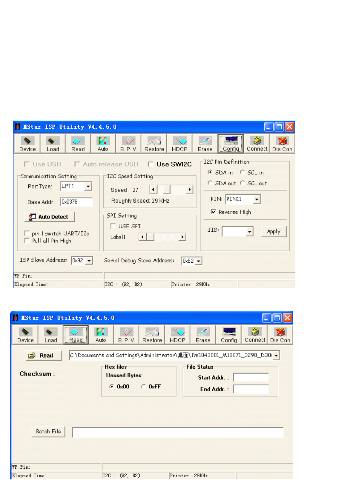
1) Execute ISP program “ Mstar ISP Utility ” and then click “ Config ” tab.
2) Set as below, and then click “ Auto Detect ” and check “ OK ” message. If display “ Error ” , Check connect computer, jig,
and set.
3) Click “ Connect ” tab. If display “ Can ’ t ” , Check connect computer, jig, and set.
4) Click “ Read ” tab, and then load download file(XXXX.bin) by clicking “ Read ” .
Page 11
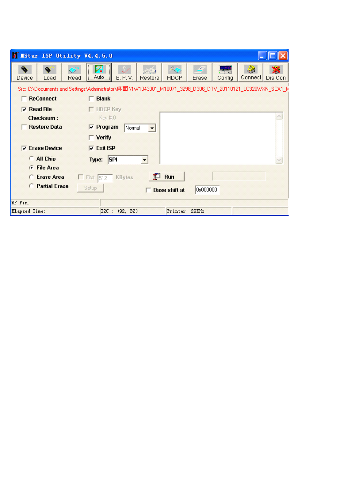
5. Click “ Auto ” tab and set as below
6. Click “ Run ” .
7. After downloading, check “ OK ” message.
Page 12
1.
TV/CATV
1.
TV/CATV
1.
1. TV/CATV
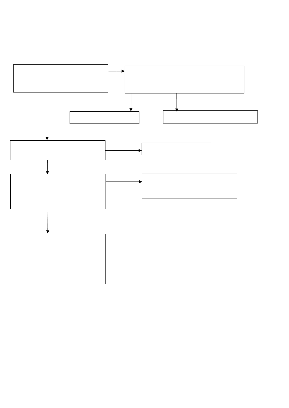
TV/CATV doesn
Check U08 PinR6/T6 (V IF ),
Can you see the normal signal?
doesn
doesn
doesn
YES
’
TROUBLESHOOTING
TROUBLESHOOTING
TROUBLESHOOTING
TROUBLESHOOTING
t
display
t
display
t
t display
display
You
should replace TUNER.
NO
Could you measure voltage of U08 & IIC lines?
Are they all normal?
YES NO
You
should check power line & IIC lines.
Check the output of U12 .
Can you see the normal waveform?
YES
Check the output of Main IC( U08 ).
Especially you should check
The VIF and IIC.
Can you see the normal waveform?
YES
This board has big problem because Main
IC( U08 ) have some troubles.
After checking thoroughly all path once
again,
You
should decide to replace Main Board
or not.
NO
NO
You
should replace TUNER.
After checking the Power of Main IC( U08 )
you should decide to replace Main IC or
not.
Page 13
2.
AV
2.
2.
2.
doesn
AV
doesn
AV
AV
doesn
doesn
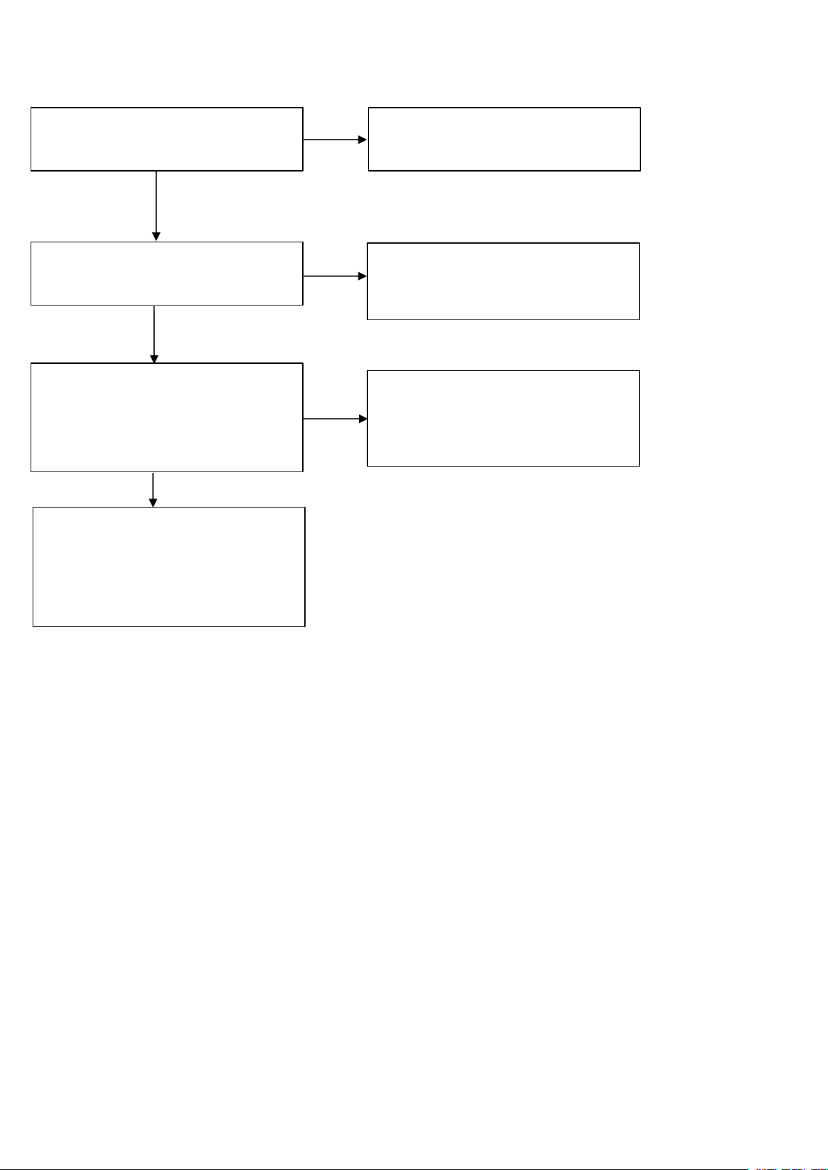
Check CN16,CN28 Can you see the
normal waveform?
t
display
t
display
t
t display
display
’
YES
NO
CN16,CN28 may have problem.
Replace this Jack .
Check the input of Main IC(U08)
Can you see the normal waveform?
YES
Check the output of Main IC(I U08 ).
Especially you should check
The VIF and IIC lines .
Can you see the normal waveform?
YES
This board has big problem because Main
IC( U08 ) have some troubles.
After checking thoroughly all path once
again,
You
should decide to replace Main
Board or not.
NO
NO
After checking the Power of Main
IC(U08)
After checking the Power of Main IC( U08 )
you should decide to replace Main IC or
not.
Page 14
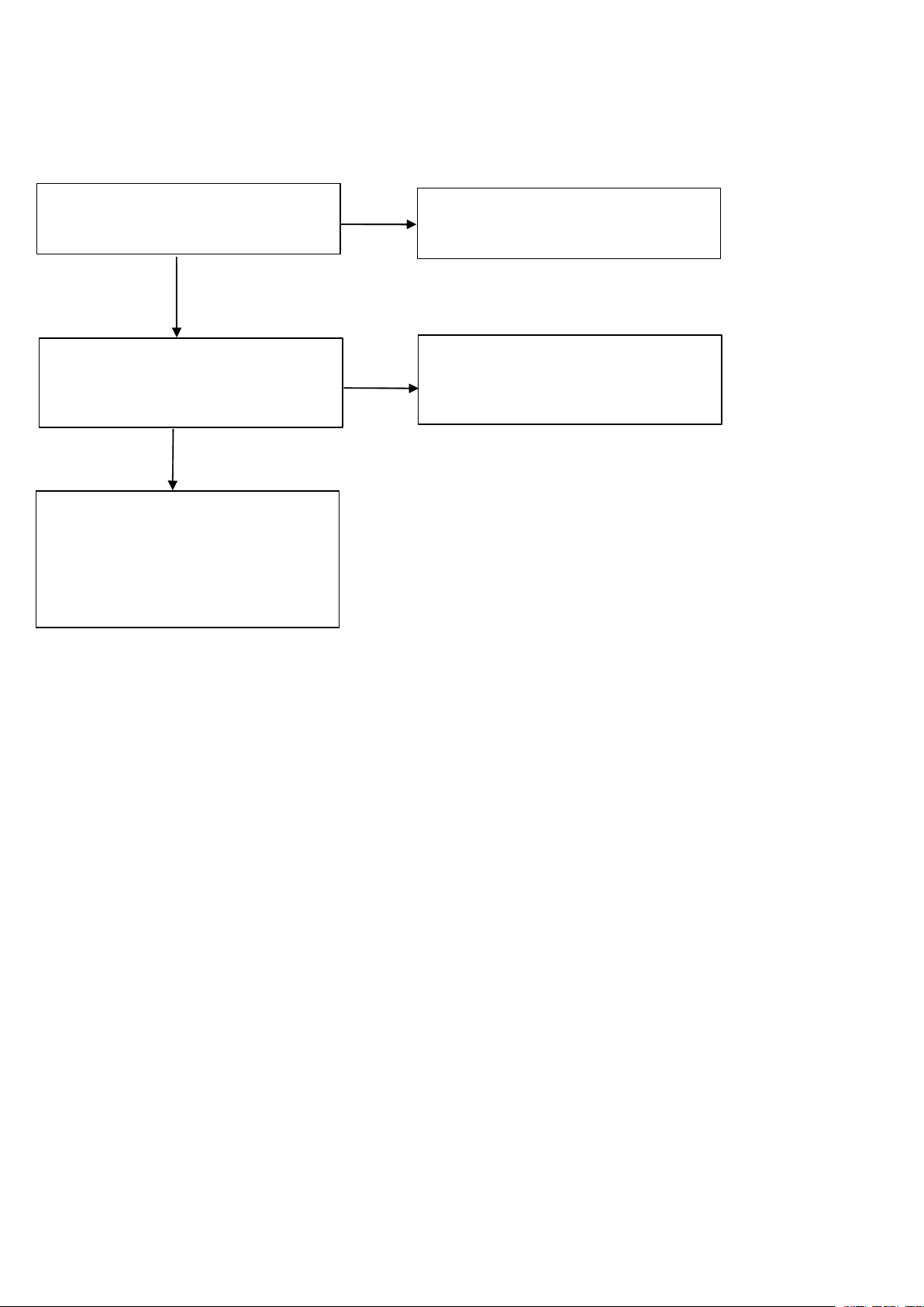
3.
Component
3.
Component
3.
3. Component
Component doesn
doesn
doesn
doesn
t
display
t
display
t
t display
display
’
Check CN24 .
Can you see the normal waveform?
YES
Check U08 an d peripheral devices ?
YES
This board has big problem because Main
IC( U09 ) have some troubles.
After checking thoroughly all path once
again,
You
should decide to replace Main
Board or not.
NO
CN24 may have problem. Replace this
Jack.
Check U08 an d peripheral devices ?
NO
Page 15
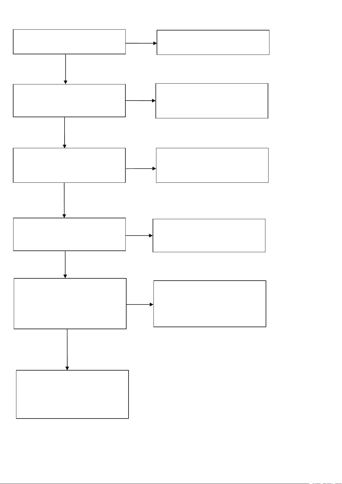
4.
RGB
4.
RGB
4.
4. RGB
RGB PC
PC
doesn
PC
doesn
PC doesn
doesn
t
display
t
display
t
t display
display
’
Check CN10 ,
Can you see the normal waveform?
YES
Check the input of RGB Video
switch( U09 ) ,Can you see the normal
waveform?
YES
Check the input of RGB switch( U09 ) ,Can
you see the normal waveform?
YES
NO
NO
NO
CN10 may have problem. Replace this
Jack.
After checking the Power of RGB Video
switch, you should decide to replace RGB
Video switch or not.
After checking the Power of RGB
switch you should decide to replace RGB
Audio switch or not.
Check the output of RGB
switch( U09 ) ,Can you see the normal
waveform?
YES
Check the output of Main IC( U08 ).
Especially you should check The H,V
sync and clock.
Can you see the normal waveform?
YES
This board has big problem because Main
IC( U08 ) have some troubles.
After checking thoroughly all path once
again,
You
should decide to replace Main
Board or not.
NO
NO
After checking the Power of RGB switch
you should decide to replace RGB Audio
switch or not.
After checking the Power of Main IC( U08 )
you should decide to replace Main IC or
not.
Page 16
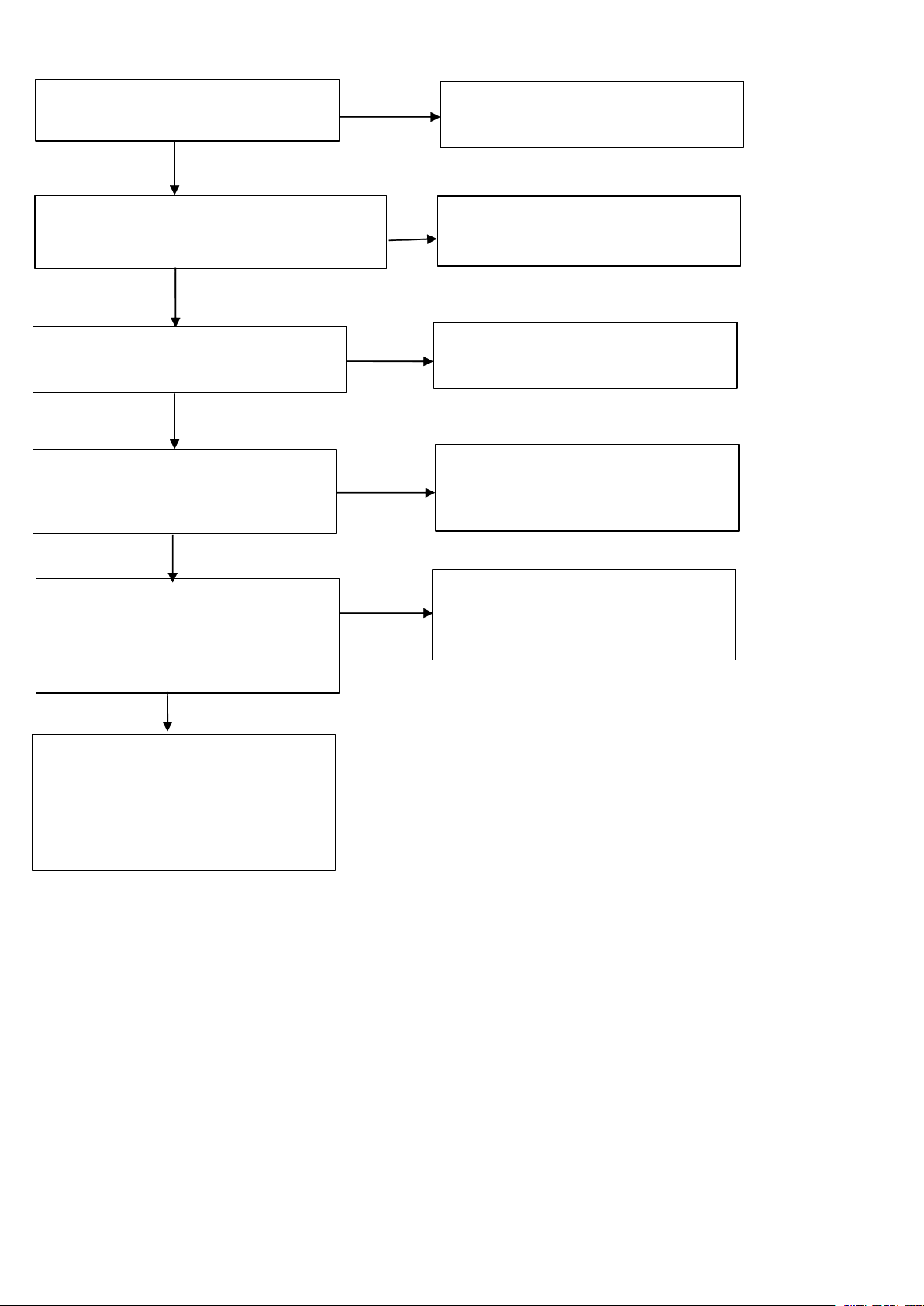
5.
HDMI
5.
HDMI
5.
5. HDMI
HDMI doesn
doesn
doesn
doesn
t
display
t
display
t
t display
display
’
Check input connect CN14 Can you see
the normal waveform?
YES
Check DDC communication
lines( CN14- Pin 15,16 )
YES
Check HDCP communication lines( U10 )
YES
Check the input of HDMI S witch ( U10 )
This signal is TMDS.Can you see the
normal waveform?
NO
NO
NO
NO
CN14 may have problem. Replace this
Jack.
After checking the Power of this chip, you
should decide to replace this or not.
After checking the Power of this chip, you
should decide to replace this or not.
After checking the trace of TMDS lines
and power of HDMI Switch, you should
decide to replace HDMI Switch or not.
YES
Check the output of Main IC( U08 ).
Especially you should check The H,V
sync and clock.Can you see the normal
waveform?
YES
This board has big problem because Main
IC( U08 ) have some troubles.
After checking thoroughly all path once
again,
You
should decide to replace Main
Board or not.
NO
After checking the Power of Main IC( U08 )
you should decide to replace Main IC or
not.
Page 17
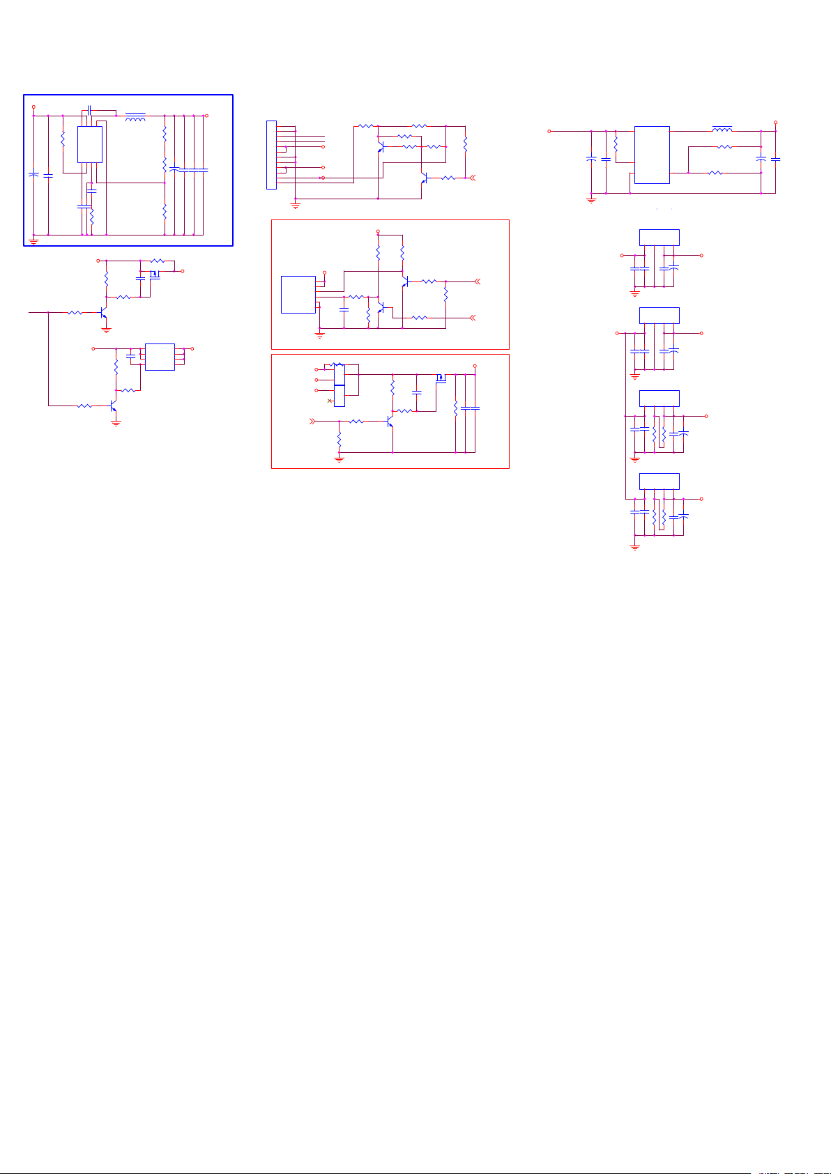
SCHEMATIC
SCHEMATIC
SCHEMATIC
SCHEMATIC DIAGRAM
DIAGRAM
DIAGRAM
DIAGRAM
+12V_PWR
CA47
470uF
STANDBY
C275
0.01uF
L33
18uH/4A
DC TO DC
DC TO DC
DC TO DC
1VI2SW3G4
R245
U4
100K
C201
FR9888
+
8
0.1uF
+12V_PWR
R141
+5V_Standby
R147
1 2
BS
FB5COMP6EN7N/C
NC
C197
C199
C202
0.1uF
R177
NC
NC
R146
R144
100K
1K
1
Q4
3904
2 3
R149
47K
R148
1K
1
Q7
3904
2 3
DC TO DC
R181
36K
R248
12K/1%
R244
10K
R140
NC/0R
Q50
AO3401A
C40.1uF
750K
1
S1
D1
2
C5
S2
D1
3
S3
D2
4
G2
D2
1u
U2
BM9435
100K
CA19
+
470uF/10V
8
7
6
5
C198
C200
0.1uF
0.1uF
+12V_NORMAL
+5V_Normal
+5V_Standby
C196
0.1uF
CN21
12p/2.0
1
2
3
4
5
6
7
8
9
10
11
12
CN02
BRI_ON/OFF
+5V_Normal
+3.3V_Normal
+12V_NORMAL
PANEL_ON/OFF
BRI_ADJ
CON6_2.0
BL-ADJUST
BL-ON/OFF
+12V_PWR
12V
12V
GND
GND
STANDBY
6
5
BL-ON/OFF
4
BL-ADJUST
3
2
1
PANEL_ON/OFF
+12V_PWR
+5V_Normal
+5V_Standby
R26
1
3
1
3
R3
220R
2 3
+5V_Normal
R131KQ3
R17NC/10K
C9
2 3
10uF
0/0603
CN03
2
NC/3*2.5*1
CN4
2
NC/3*2.5*1
R20 4.7K
R21
10K
IO ,
R4
2.7K
R8
NC/1K
Q31
R6
R7
1K
3904
1
Q30
3904
2 3
R42
R10
1K
1K
Q28
1
R12
3904
2 3
3904
1
R16 4.7K
AO3401A
R18
C100.22uF
10K
R19
10K
Q5
1
3904
2 3
4.7K
1
1K
VBL_CTRL
1K
R14NC/10K
BRI_ADJ-PWM0
Q48
PANEL_ON
R2
PM GPIO
VCC-Panel
R28
22K
R1
4.7K
C11
0.1uF
PWR-ON/OFF
VBL_CTRL
BRI_ADJ-PWM0
C15
0.1uF
+5V_Normal
+
CA4
470uF/10V
+5V_Standby
+5V_Normal
U01
FP6161
4
IN
R33
C80.1uF
1
EN
47K
GND2FB
Vout=0.6V*(1+R1/R2)
Vout=0.6V*(1+R1/R2)
Vout=0.6V*(1+R1/R2)
Vout=0.6V*(1+R1/R2)
Vout=0.6V*(1+15/12)
Vout=0.6V*(1+15/12)
Vout=0.6V*(1+15/12)
Vout=0.6V*(1+15/12)
U03 BM1117 -3.3
IN
321
C25
C31
4.7uF
0.1uF
U04 BM1117 -3.3
IN
321
C34
C33
0.1uF
4.7uF
U05
BM1117
IN
321
C17
C16
R24
0.1uF
4.7uF
560R
U06
BM1117
IN
321
C26
C19
R25
4.7uF
0.1uF
100R
SW
ADJ
4
C24
0.1uF
ADJ
4
C32
0.1uF
ADJ
4
R22
560R
ADJ
4
R23
220R
18uH/2A
3
R11 15K_1%
R1
R1
R1
5
R15 12K_1%
OUT
OUT
150mA
+3.3V_Standby
+
CA9
100uF
OUT
OUT
300mA
+3.3V_Normal
+
CA10
470uF/10V
OUT
OUT
300mA
+2.5V_Normal
+
C18
CA5
0.1uF
470uF/10V
OUT
OUT
1.8V
AVDD_DDR
+
CA6
C20
0.1uF
470uF/10V
+1.2V_VDDC
L40
1000mA
12
R2
R2
R2
R2R1
CA3
+
C70.1uF
470uF/10V
Page 18
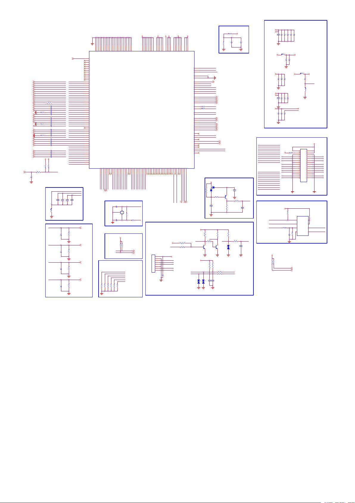
IC MST6M181VG,MST6M182VG ,
BALL D5 BALL B4 NC PIN;
MST6M161LG PIN HDMI INPUT
HDMI_HP1
HDMI_HP1
HDMI1-CLKN
HDMI1-CLKN
HDMI1-CLKP
HDMI1-CLKP
HDMI1-RX0N
HDMI1-RX0N
HDMI1-RX0P
HDMI1-RX0P
HDMI1-RX1N
HDMI1-RX1N
HDMI1-RX1P
HDMI1-RX1P
HDMI1-SDA D DCDA_DA
HDMI1-SDA
HDMI1-RX2N
HDMI1-RX2N
HDMI1-RX2P
HDMI1-RX2P
HDMI1-SCL DDCDA_C K
HDMI1-SCL
VGA_HS
RGB0_Pb+
RGB0_Y-SOG
RGB0_Y+
RGB0_Pr+
VGA_VS
RGB2-HDTV_BIN
RGB2-HDTV_SOGIN
RGB2-HDTV_GIN
RGB2-HDTV_RIN
AV2_in
AV1_in
AV3_in
CVBS_OUT0
AV1_AULin0
AV1_AURin0
VGA-AULin0
VGA-AURin0
AV2_AULin2
AV2_AURin2
AV3_AULin2
AV3_AURin2
TAGC
ARC
ARC
VGA_HS
RGB0_Pb+
RGB0_Y-SOG SOGIN 0
RGB0_Y+
R110 68R
RGB0_Pr+
VGA_VS
RGB2-HDTV_BIN BIN2
RGB2-HDTV_SOGIN
RGB2-HDTV_GIN
R112 68R
RGB2-HDTV_RIN
AV1_in
AV3_in
R114 68R
AV1_AULin0
AV1_AURin0
AV3_AULin2
AV3_AURin2
+5V_Tuner
R135 10K
C1 6922 nF
Close IC
R107 0
C125 47nF
C126 1nF
C127 47nF
C128 47nF
C129 47nF
C130 47nF
C131 1nF
C132 47nF
C133 47nF
C134 47nF
C150 47nF
C151 47nF
C143 47nF
C144 47nF
C145 2.2uF
C147 2.2uF
C152 2.2uF
C156 2.2uF
C171 2.2uF
C170 2.2uF
C179 2.2uF
C195 2.2uF
+3.3V_TU
R1 3410K
HDMI1-ARC
BIN0
GIN0P
GIN0M
RIN0
SOGIN2
GIN2P
GIN2M
RIN2
CVBS2P
CVBS1P
CVBS0P
VCOM0
CVBS_OUT0
AUL2AV2_AULin2
AUR2AV2_AU Rin2
AUL3
AUR3
R1 3910K /NC
AGCTAGC
Audio
C1 5810 uF
C1 590.1 uF
Close to IC
Close to IC
Close to IC
Close to IC
L10 3FB/060 3
with width trace
with width trace
with width trace
with width trace
AV-AUOUTL3 AV_AUOUTL3
C1 64180 pF
AV-AUOUTR3
C1 66180 pF
AMP-AUOUTR0
C1 67180 pF
C1 68180p F
DDR2 VREF
Normal Power 1.2V
Normal Power 1.2V
Normal Power 1.2V
Normal Power 1.2V
VDDC
R1041K_1%
VD DC
K11
A12
F13
G13
N6
GN D
GN D
GN D
GN D
GN D
MST6M181VG
MST6M181VG
MST6M181VG
MST6M181VG
MST6M182VG
MST6M182VG
MST6M182VG
MST6M182VG
MST6M161LG
MST6M161LG
MST6M161LG
MST6M161LG
R_ OD D2 /LVB 2P
G_O DD 3/ LV A0M
G_O DD 4/ LV B4P
G_O DD 5/ LV B4M
G_O DD 6/ LV B3P
G_O DD 7/ LV B3M
G_O DD 2/ LV A0P
G_O DD 1/ LV A1M
R_ OD D0 /LVB CK P
R_ OD D1 /LVB CK M
R_ OD D3 /LVB 2M
T14
T15
P14
P15
P16
N1 4
R1 4
R1 5
R1 6
N1 5
M1 4
RX E0 +
RX O3 -
RX OC +
RX O3 +
RX O2 -
RX O1 +
RX OC -
RX O2 +
RX E0 -
XTALI
R1 201M
XTALO
R131 75
UART-RX
UART-RX
UART-TX
UART-TX
4'h0
4'h0
4'h0
4'h0
4'h3
4'h3
4'h3
4'h3
4'h7
4'h7
4'h7
4'h7
L8
VD DC
VD DCL7VD DCK8VD DCK7VD DCJ8VD DCJ7VD DC
1.26V
1.26V
1.26V
1.26V
GP IO2 1/TC ON 21 /VG H_ OD D_4 9
GP IO2 0/TC ON 20 /VG H_ EVE N _48
GP IO1 9/TC ON 19 /GC LK 6_47
R_ OD D4 /LVB 1P
R_ OD D5 /LVB 1M
R_ OD D6 /LVB 0P
R_ OD D7 /LVB 0M
L15
L16
K14
K16
M1 5
M1 6
RX O0 +
RX O0 -
RX O1 -
H1 1
J10
J11
K10
P7
H1 0
GN DR7GN DT7GN DH9GN D
GN DJ9GN D
GN D
GN D
RF AG CT4B_O D D2 /LV A3P
VIF MR6VIF P
B_O D D5 /LV AC KM
B_O D D0 /LV A4P
B_O D D1 /LV A4M
B_O D D3 /LV A3M
B_O D D4 /LV AC LP
T6
P11
P12
P10
T11
T12
R1 0
R1 1
VIF P
AG C
RX E3 +
RX E3 -
RX EC -
RX E2 +
RX EC +
VIF P
VIF M
System XTAL
C157 33pF
C163 33pF
Debug port
+5V_Standby
BRI_ADJ-PWM0
Tuner_PWM
AUMCK_OUT
AUBCK_OUT
R1 374.7K
R1 504.7K
R1 25NC/4. 7K
R1 234.7K
R1 24NC/4. 7K
GN DK9GN D
B_O D D7 /LV A2M
G_O DD 0/ LV A1P
B_O D D6 /LV A2P
P13
R1 2
R1 3
RX E1 -
RX E2 -
RX E1 +
X0124M Hz
3
1 2
R1 174.7K
R1 184.7K
J14AMP-AUOUTL0
J15
AV_AUOUTL3
AV_AUOUTR3
AMP_AUOUTR0
AMP_AUOUTL 0
GN DG1GN DG2GN DG3GN DP4GN DR4GN DR5GN DT5GN DP6GN D
D6
CEC
D5
HOTPLUGD
C7
RXCKN_D
B7
RXCKP_D
C6
RX0N_D
B6
RX0P_D
A6
RX1N_D
C5
RX1P_D
C4
DDCDD_DA
A5
RX2N_D
B5
RX2P_D
B4
DDCDD_CK
D4
HOTPLUGA
A3
RXCKN_A
A2
RXCKP_A
B3
RX0N_A
B2
RX0P_A
B1
RX1N_A
C3
RX1P_A
D3
DDCDA_DA
C1
RX2N_A
C2
RX2P_A
D1
DDCDA_CK
D2
ARC
E4
HSYNC0
E3
BIN0P
E2
SOGIN0
F3
GIN0P
F2
GIN0M
F1
RIN0P
F4
VSYNC0
H3
BIN1P
H2
SOGIN1
J3
GIN1P
J2
GIN1M
J1
RIN1P
K3
VSYNC1
K1
CVBS2
K2
CVBS1
L1
CVBS0
L2
VCOM
M1
CVBSOUT
M2
AUL0
N1
AUR0
N2
AUL1
P1
AUR1
L3
AUVAG
M4
AUREFM
P2
AUL2
R1
AUR2
M3
AUL3
N3
AUR3
N4
AUOUTL1
P3
AUOUTR1
R2
AUOUTL0
T2
AUOUTR0
XINT3XO UT
PG A-C OM
MST6M161LG
P5
R3
VIF M
XT ALI
XT ALO
AV SS _P GA
{I2S_OUT_BCK,I2S_OUT _MCK,PWM1,PWM0}
{I2S_OUT_BCK,I2S_OUT _MCK,PWM1,PWM0}
{I2S_OUT_BCK,I2S_OUT _MCK,PWM1,PWM0}
{I2S_OUT_BCK,I2S_OUT _MCK,PWM1,PWM0}
B51_no_EJ
B51_no_EJ
B51_no_EJ
B51_no_EJ
B51_Secure_no_scramb le
B51_Secure_no_scramb le
B51_Secure_no_scramb le
B51_Secure_no_scramb le
B51_Secure_scramble
B51_Secure_scramble
B51_Secure_scramble
B51_Secure_scramble
R1 224.7K
HDMI-CEC
HDMI-CEC
HDMI_HP1
HDMI1-CLKN
HDMI1-CLKP
HDMI1-RX0N
HDMI1-RX0P
HDMI1-RX1N
HDMI1-RX1P
DDCDA_DA
HDMI1-RX2N
HDMI1-RX2P
DDCDA_CK
HDMI1-ARC
VGA_HS
BIN0
SOGIN0
GIN0P
GIN0M
RIN0
VGA_VS
BIN2
SOGIN2
GIN2P
GIN2M
RIN2
CVBS2P
CVBS1P
CVBS0P
VCOM0
CVBS_OUT0
AUL0
AUR0
AUL1
AUR1
AUVAG
AUVRM
AUL2
AUR2
AUL3
AUR3
AV-AUOUTL3
AV-AUOUTR3
AMP-AUOUTL0
AMP-AUOUTR0
AUVRM
AUVRP
AUVAG
C1 6210 uF
C1 600.1 uF
R1 21100 K
AV_AUOUTR3
R1 2610 0K
AMP_AUOUTR0
R1 27100 K
AMP_AUOUTL 0
R1 33100 K
AD C2 P5
+2.5 V_ PG A
AV DD _D DR
N5
H6
M5
K6
H8
H7
E13
M1 1
M1 0
J6
G8
AV DD _2 5
AV DD _1 P2
AV DD _P GA
AV DD _R EF
AV DD _D DRD9AV DD _D DR
AV DD _D DR
AV DD _D DR
AV DD _D DR
AV DD _A U2 5
DDR1 2.5V
2.5V
DDR1 2.5V
2.5V
DDR1 2.5V
DDR1 2.5V
2.5V
2.5V 3.3V
DDR2 1.8V
DDR2 1.8V
DDR2 1.8V
DDR2 1.8V
GPIO define
GPIO define
GPIO define
GPIO define
MST6M161LG/MST6M181VG
MST6M161LG/MST6M181VG
MST6M161LG/MST6M181VG
MST6M161LG/MST6M181VG
MST6M182VG
MST6M182VG
MST6M182VG
MST6M182VG
GP IO1 1/TC ON 11 /HC ON _39
GP IO1 0/TC ON 10 /OP T_N _3 8
GP IO9 /TC ON 9/O PT _P_ 37
GP IO8 /TC ON 8/FL K3 _36
GP IO1 8/TC ON 18 /GC LK 5_46
GP IO1 7/TC ON 17 /GC LK 4_45
GP IO1 6/TC ON 16 /WPW M _44
GP IO1 3/TC ON 13 /LED O N_41
GP IO1 5/TC ON 15 /SCA N_ BL K1_ 43
GP IO1 4/TC ON 14 /SCA N_ BL K_4 2
GP IO1 2/TC ON 12 /DPM _4 0
GP IO6 /TC ON 6/FL K_ 34
GP IO7 /TC ON 7/FL K2 _35
GP IO5 /TC ON 5/S OE_ 33
J16
L14
J15
F16
K15
F15
F14
E14
D1 5
G15
H1 6
G16
D1 4
D1 6
H1 5
J15
IR&Key_Pad
+5V_Normal
KEYBOARD
8P/2.0
+5V_Standby
8
7
6
5
4
3
2
1
CN05
+5V_Standby
IR-in
LED_R
LED-G
K1
K0
C1 650 .1u
AV DD _3 3
J5
L5
L6
AV DD _P LL
AV DD _M OD
AV DD _M ODK5AV DD _M ODM6AV DD _M OD
AV DD _A U3 3
3.3V
3.3V
3.3V
SAR2_GPIO13 /GPIO73
SAR1_GPIO12 /GPIO74
SAR0_GPIO11 /GPIO75
PWM0_GPIO20/ GPIO26
PWM1_GPIO21/ GPIO25
PMGPIO_G PIO10/GPIO66
PM1_GPIO 6/GPIO67
PM4_GPIO 7/GPIO68
PM5_GPIO 8/GPIO69
PM6_GPIO 9/GPIO70
SAR3_GPIO14 /INT_GPIO65
DDCR_CK/GPI O63
DDCR_DA/GPI O64
GP IO3 /TC ON 3/G CL K2_ 31
GP IO2 /TC ON 2/G CL K1_ 30
GP IO4 /TC ON 4/G CL K3_ 32
GP IO1 /TC ON 1/V ST_ 29
GP IO0 /TC ON 0/P OL_ 28
GP IO3 0/LC K_7 4
J14
E16
E15
H1 4
N1 0
N1 1
J14
LED
HD _S W
R732 2.7K
LED
R151 100
AV DD _3 3_P M
H4
J4
K4
AV DD _3 3
AV DD _D VI
AV DD _D MP LL
DVDD_NODIE
GND_EFUS E
HWRESET
NC/GPIO6 2
GPIO26/G PIO61
GPIO27/G PIO60
NC/GPIO5 9
GPIO23/G PIO58
GPIO25/G PIO57
GPIO24/G PIO56
GPIO22/G PIO55
GP IO2 9/LD E_7 5
GP IO2 8/LH SY NC
GP IO2 7/LVS Y NC
N1 2
N1 3
DV D_ IR
DV D_ ON /OF F
MDDR_VREF
K13
MVREF
DVDD_NODIE_ 1.2V
D7
AUVRP
L4
VRP
D13
C13
TESTPIN
LED_G
C10
KEY0-SAR1
C11
KEY0-SAR0
B11
B15
SCZ
SPI-SDO SPI _Flash-SDO
B16
SDO
SPI-SDI SPI _Flash-SDI
C16
SDI
SPI-SCK SPI_Flash-SCK
C15
SCK
B13
USB1_DP
A13
USB1_DM
A14
USB0_DP
A15
USB0_DM
R108 68R
D11
DDCA_DA
R109 68R
D10
DDCA_CK
B9
IRIN
A9
BRI_ADJ-PWM0
B12
Tuner_PWM
C12
SPI_WP0N
D12
PANEL_ON/OF F
A11
PWR-ON/OFF
A10
VBL_CTRL
B10
AMP-MUTE
C9
G14
TUNER_SCL
B14
TUNER_SDA
C14
N9
USB_ON1
P9
SPDIF_OUT
T9
N8
P8
AUBCK_OUT AU BCK_I2S_OUT
R9
AUMCK_OUT AUMCK_I2S_OUT
R8
T8
IC M ST6M181VG,MST6M182VG ,
BALL N8 BALL N9 NC PIN.
U08
RESET CIRCUIT
+5V_Standby
R1 362.7K
LED_R
R142 1K
1
2 3
+3.3V_Standby
K0
K1
D1 03N C
D1 02N C
1 2
1 2
IC MST6M181VG,MST6M182VG ,
R104,R106,C114 ;
IC MST6M161LG ,
R104,R106,C114 .
SC_FS
SPI_CS0N
USB2_DP
USB2_D+
USB2_DM
USB2_D-
USB0_DP
USB1_D+
USB0_DM
USB1_D-
UART-TX
UART-RX
IRIN
System-RST
BRI_ADJ-PWM0
Tuner_PWM
PANEL_ON/OF F
PWR-ON/OFF
VBL_CTRL
AMP-MUTE
+5V_Standby
RESET
3
2
D100
BAV99
R1 011M
R102 4.7K
1
C1 114. 7uF
R1 432.7K
LED-G
Q102
1
Q100
3904
3904
2 3
R1 2810K
R1 15710K
R129 100
R1158 100
C1 000. 1u
C9 210. 1u
MDDR_VREF
C1 130.1 uF
R1 061K_ 1%
USB_ON1
SPDIF_OUT
C1 012.2 uF
Q101
1
3906
R103 1K
3 2
R1 0522K
R1 1610K
IR-in IRIN
R119 68R
D1 01NC
1 2
KEY0-SAR0
KEY0-SAR1
AVDD_DDR
C1 141nF
System-RST
C1 121n F
C1 6133p F
Chip Config
+1.2V_VDDC
C1 022.2 uF
C1 040.1 uF
C1 030.1 uF
Normal Power 2.5V
Normal Power 2.5V
Normal Power 2.5V
Normal Power 2.5V
L101 FB/0603
+2.5V_Normal
250mA
C1 150.1 uF
DDR power
DDR power
DDR power
DDR power
AVDD_DDR
C1 2410u F
C1 220.1 uF
C1 230.1 uF
Normal Power 3.3V
Normal Power 3.3V
Normal Power 3.3V
Normal Power 3.3V
AVDD_33
+3.3V_Normal
+3.3V_Standby
C1 362.2 uF
Standby Power 3.3V
Standby Power 3.3V
Standby Power 3.3V
Standby Power 3.3V
C1 530.1 uF
R7_RXO0-RXO0R6_RXO0+RXO0+
R5_RXO1-RXO1R4_RXO1+RXO1+
+5V_Normal
R3_RXO2-RXO2R2_RXO2+RXO2+
R1_RXOC-RXOCR0_RXOC+R XOC+
G7_RXO3-RXO 3G6_RXO3+RXO3+
G3_RXE0-R XE0G2_RXE0+RXE0+
G1_RXE1-R XE1G0_RXE1+RXE1+
B7_RXE2-RXE2B6_RXE2+RXE2+
B5_RXEC-RXECB4_RXEC+RXEC+
B3_RXE3-RXE3B2_RXE3+RXE3+
C1 380.1 uF
C1 370.1 uF
C1 552.2 uF
C1 540.1 uF
Connector
R6_RXO0+
R4_RXO1+
R2_RXO2+
G6_RXO3+
G0_RXE1+
B6_RXE2+
B4_RXEC+
B2_RXE3+
SERIAL FLASH
+3.3V_Standby
SPI_CS0N
SPI_Flash-SDO
SPI_WP0N SPI_Flash-SCK
+5V_Tuner
R1 304.7 K
R1131K
R1 324.7 K
TUNER_SDA
TUNER_SCL
C1 060.1 uF
C1 050.1 uF
C1 160.1 uF
C1 350.1 uF
DVDD_NODIE_ 1.2V
R1 114.7K
FLASH_CS0N
FLASH_WP0N
C1 460.1 uF
R1 1510K
TUNER_SDA
TUNER_SCL
C1 070.1 uF
R14547K
ADC2P5
U07
1
2
3
AVDD_33_PM
2
2
4
4
6
6
8
8
10
10
12
12
14
14
16
16
18
18
20
20
22
22
24
24
26
26
28
28
30
30
DIP\30\2X20
CN06
CE#
SO
WP#
VSS4SI
EN25Q32
L100FB/0603
+2.5V_PGA+2.5V_Normal
C1 180.1 uF
AVSS_PGA
L10 2FB /0603
VCC-Panel
1
1
3
3
5
5
R7_RXO0-
7
7
R5_RXO1-
9
9
R3_RXO2-
11
11
13
13
R1_RXOC-R0_RXOC+
15
15
G7_RXO3-
17
17
G3_RXE0-G2_RXE0+
19
19
G1_RXE1-
21
21
B7_RXE2-
23
23
25
25
B5_RXEC-
27
27
B3_RXE3-
29
29
8
VDD
7
HOLD#
6
SCK
SPI_Flash-SDI
5
Page 19
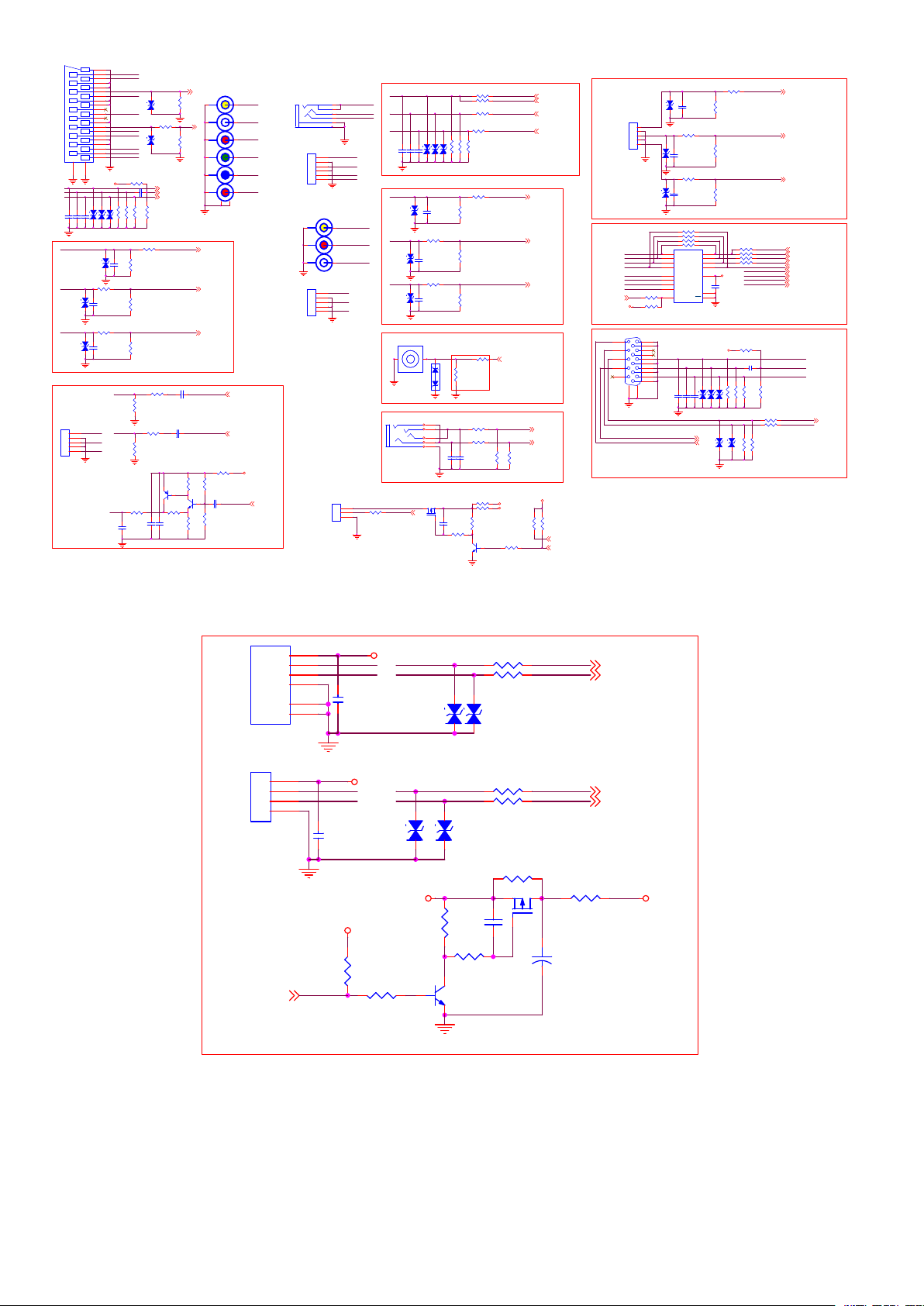
CN23
NC/5p/2.0
CN15
SCART/NG
21
AV2_V
20
AV_VOUT
SCART INPUT
Blanking I/O
SCART-Rin
SCART-G
Switch
SCART-Bin
AV2_L
AV_LOUT
AV2_R
AV_ROUT
R524 100K
R522
R523
D506
1 2
NC
75R
75R
D505
C186
NC
NC
AV_ROUT
AV_LOUT
AV_VOUT
C50433pF
SCART INPUT
SCART INPUT
SCART INPUT
SC_FB
R232
D143
75R
1 2
NC
SC_FS
R230 10K
D127
R231
1 2
NC
2.7K
SCART-Rin
C507 4.7uF
SCART-Gin
SCART-Bin
R533
R534
75R
100K
SCART RGB
AV2_in
R532 33R
R514
75R
AV2-L
R517
12K
AV2-R
R519
AV input 2
12K
C502 2.2u
R516 47R
R500
10K
R520 47R
C503 2.2u
R521
AVOUT
10K
3906
Q501
3904
Q500
R52875R
R52975R
C505
C506
2.2u
0.1u
2 3
SC_FB
AV_AUOUTR3
AV_AUOUTL3
R526330R
R530
75R
SC_FS
10
11
12
AV2_in
AV2_AULi n2
AV2_AURin2
1
1
445
778
10
11
12
R535 10R
R527
47K
R531
33K
CN28 6P RCA INPU T
SCART-G
221
SCART-Bin
5
SCART-Rin
8
AV2_V
3
3
AV2_L
6
6
AV2_R
9
9
131314
14
AV_AUOUTR3
AV_AUOUTL3
CVBS_OUT0
C50010uF
+5V_Normal
CVBS_OUT0
5
1
3
2
6 7
CN24PJ
CN27
HD_Y
1
2
HD_Pb
3
4
HD_Pr
5
SPDIF
6
NC/6P/2.0
CN16
AV1_V
2
552
4
334
1
661
3P RCA INPU T
CN20
AV1_V
1
2
AV1_L
3
4
AV1_R
5
NC/5p/2.0
CN19
CON4_2.0
1
2
3
AV1_L
AV1_R
HD_Pb
HD_Pr
R431 1K
IR
HD_Pb
HD_Pr
R509
R508
D504
D502
D503
C180
C181
C182
1 2
1 2
1 2
NC
NC
NC
NC
NC
NC
AV1_V
D501
NC
AV1_L
1 2
AV1_R
1 2
2 1
2 1
CN09
PJ325
5V
75R
75R
C191
1 2
NC
R507 10K
D511
C189
NC
NC
R512 10K
D512
C190
NC
NC
CN9RCA1
CN08RCA1
Coaxial Output
Coaxial Output
Coaxial Output
Coaxial Output
SPDIF
R158150R
DD31
NC
4
PC-L
2
1
PC-R
PC-R
3
5
C177
NC
Q47 AO 3401A
DVD_IR
C130. 1u
3904
HD_Y
HD_Y
4
RGB2-HDTV _GIN
R502 33R
RGB2-HDTV _SOGIN
R503 33R
RGB2-HDTV _BIN
R505 33R
RGB2-HDTV _RIN
R506 33R
R510
YPbPr
75R
AV1_in
R501 33R
R504
75R
AV1_AULi n0
R511
12K
AV1_AURin0
AV input1
R513
12K
R82330R
SPDIF_OUT
CLOSED TO MST6M181CS
VGA audio input
C178
NC
R396 10K
R397 10K
NC
R43750K
Q29
2 3
VGA-AULin0
VGA-AURin0
R294
R295
12K
12K
R473 30
+3.3V_Normal
R44
+5V_Normal
R27
47K
1
RGB2-HDTV _GIN
RGB2-HDTV _SOGIN
RGB2-HDTV _BIN
RGB2-HDTV _RIN
AV1_in
AV1_AULi n0
AV1_AURin0
VGA-AULin0
VGA-AURin0
+3.3V_Normal
R1162
R1166
4.7K
4.7K
DVD_IR
R491K
DVD_ON/O FF
HD_SW
+3.3V_Normal
15
14
13
12
11
CN-2.0-5P
VGA-G
VGA-Bin
VGA-Rin
VGA_V
SCART-Gin
SCART-Bin
SCART-Rin
SC_FB
16
1 2
CN11
AV3_V
1
2
AV3_L
3
4
AV3_R
5
5p/2.0
D515
1 2
NC
D513
1 2
NC
11
14
10
13
HD_SW
R215 100R
R216 4.7K
CN10
5
10
4
9
3
8
2
7
1
6
VGA
17
VGA-HS
VGA-VS
VGA-SDA
D514
C193
NC
NC
R544 10K
C194
NC
R539 10K
C192
NC
R208
R206
R96
R98
U09 NC/CBT 3257A
2
S1A
5
S1B
S1C
S1D
3
S2A
6
S2B
S2C
S2D
1
IN
VGA RGB
VGA-Bin
VGA-Gin
VGA-Rin
NC
UART-TX
UART-RXVGA-SCL
R543 33R
R541
75R
R540
12K
AV input 3
R542
12K
0
0
0
0
R606 33R
R607 33R
4
DA
7
R605 33R
DB
9
R608 33R
DC
12
DD
16
+5V_Normal
VCC
C141
8
GND
15
EN
0.1u
RGB switch
R34 1 00K
+5V_Normal
D601
D600
D602
R609
R610
C142
C148NCC149
1 2
1 2
1 2
NC
NC
NC
NC
75R
75R
D603
D604
UART-TX
UART-RX
1 2
1 2
NC
NC
SCART-Gin
SCART-Bin
SCART-Rin
SC_FB
C98 4.7uF
R611
75R
R615
10K
AV3_AURin2
R616
10K
AV3_AULi n2
RGB0_Y+
RGB0_Y-SOG
RGB0_Pb+
RGB0_Pr+
VGA_VS
R612100k
R613 68R
R614 68R
AV3_in
AV3_AULi n2
AV3_AURin2
RGB0_Y+
RGB0_Y-SOG
RGB0_Pb+
RGB0_Pr+
VGA_VS
SCART-Gin
SCART-Bin
SCART-Rin
SC_FB
VGA-G
VGA_HS
VGA_HS
VGA_V
AV3_in
19
18
17
16
15
14
13
12
11
10
9
8
7
6
5
4
3
2
1
23
22
+5V_Normal
SCART-G
D507
D508
C183NCC184NCC185
1 2
1 2
NC
NC
NC
AV2_V
1 2
AV2_L
R515 10K
D509
C187
1 2
NC
NC
AV2_R
R518 10K
D510
C188
1 2
NC
NC
AV_VOUT
1
2
AV_LOUT
3
4
AV_ROUT
5
CN12
1 VCC
2 D-
3 D+
4 GND
SHIELD
SHIELD
USB_4P
USB1
CN13
CN-2.0-4PAA
USB2
USB_ON1
1
2
3
4
1
USB1_D1-_in
2
USB1_D1+_in
3
4
5
6
USB2_D1+_in
USB2_D1-_in
C9410uF
USB_ON1
C9710uF
+5V_USB
+3.3V_Normal
R13810K
R31 4.7K
+5V_USB
USB1_D1-_in
USB1_D1+_in
USB2_D1-_in
USB2_D1+_in
D627NC
1 2
1 2
D626NC
1 2
D628NC
R629 5. 1R
R627 5. 1R
D625NC
1 2
R625 5. 1R
R628 5. 1R
USB1_DUSB1_D+
USB2_DUSB2_D+
USB1_DUSB1_D+
USB2_DUSB2_D+
R35 R56/0805
AO3401A
+5V_Normal +5V_USB
R547K
Q49
C120.1u
R32 750K
Q6
1
3904
CA11NC/100uF
+
R36 R22/0805
2 3
Page 20
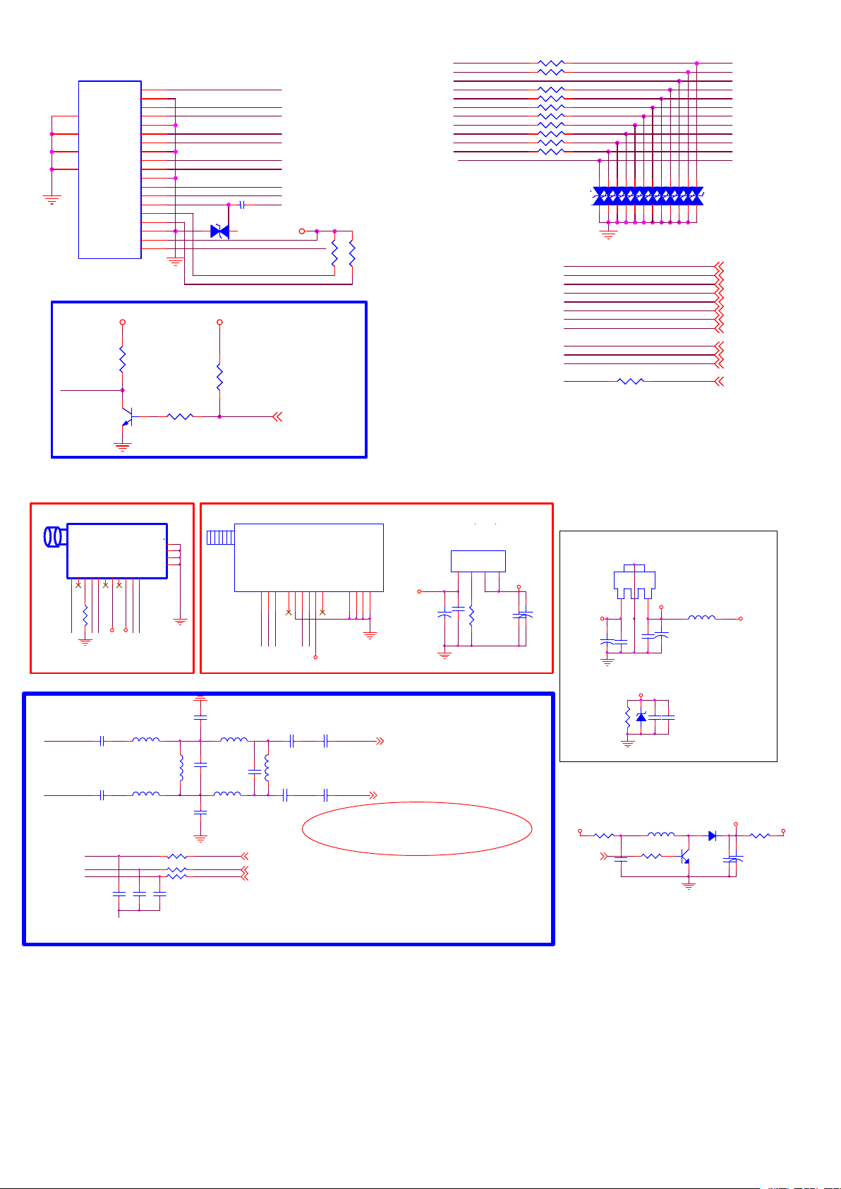
GND1
GND2
GND3
GND4
CN14
DATA2 SHIELD
20
DATA1 SHIELD
21
22
DATA0 SHIELD
23
DDC/CEC GND
HPD_SINK
HDMI2
HDMI2
HDMI2
HDMI2
DATA2+
DATA2-
DATA1+
DAT1A-
DATA0+
DATA0-
CLK SHIELD
+5V POWER
HOT PLUG
HDMI_J
CLK+
CLKCEC
NC
SCL
SDA
HDMI2_5V
R931K
D640NC
1 2
1 2
HDMI1-RX2P
HDMI1-RX2N
HDMI1-RX1P
HDMI1-RX1N
HDMI1-RX0P
HDMI1-RX0N
HDMI1-CLKP
HDMI1-CLKN
HDMI1-SCL
HDMI1-SDA
ARC
R709 220R
SDA2
SCL2
HPD2HPD_SINK
IN2D2+
IN2D2IN2D1+
IN2D1IN2D0+
IN2D0IN2CLK+
IN2CLK-
D629NC
1 2
D630NC
D631NC
D632NC
D633NC
D634NC
D635NC
D636NC
D637NC
D638NC
D639NC
1 2
1 2
1 2
1 2
1 2
1 2
1 2
1 2
1 2
HDMI1-RX2P
HDMI1-RX2N
HDMI1-RX1P
HDMI1-RX1N
HDMI1-RX0P
HDMI1-RX0N
HDMI1-CLKP
HDMI1-CLKN
HDMI1-SCL
HDMI1-SDA
HDMI-CECCEC
ARC
HDMI-CEC
HDMI1-SDA
HDMI1-SCL
C88 1u
D641 NC 12
SCL2
SDA2
+3.3V_Normal
R7410K
HDMI2-RX2+ I N2D2+
HDMI2-RX2- IN2D2-
HDMI2-RX1+ I N2D1+
HDMI2-RX1- IN2D1-
HDMI2-RX0+ I N2D0+
HDMI2-RX0- IN2D0-
HDMI2-RXC+ I N2C LK+
HDMI2-RXC- IN2CLK-
CEC
ARC
HDMI2_5V
HOTPLUG
HOTPLUG
HOTPLUG
HOTPLUG
HPD2
R7910K
R8010K
1
2
3
4
5
6
7
8
9
10
11
12
13
14
15
16
17
18
19
HDMI1-RX2P
HDMI1-RX2N
HDMI1-RX1P
HDMI1-RX1N
HDMI1-RX0P
HDMI1-RX0N
HDMI1-CLKP
HDMI1-CLKN
CEC
R251 5R 1
R249 5R 1
R254 5R 1
R250 5R 1
R253 5R 1
R257 5R 1
R255 5R 1
R256 5R 1
R258 5R 1
R259 5R 1
ET-6N1E-CF101R
AGC1NC12AS3SCL4SDA55VA65VB7NC3833V9NC410IFout
AS
R306
TU_SCL
TUAGC
TU_SDA
68R
IF-IN-
Q10
3904
TU2
C3570.1u
C3650.1u
BPF_IN
BPF_IN
BPF_IN
BPF_IN
IF-IN-
+5V_Tuner
33V
132R76 4. 7K
GND1
GND4
GND2
GND3
11
IF-IN+
TUNER AGC,Close TUNER
TUAGC
TU_SDA
TU_SCL TUNER_SCL
R803 100R
R805 100R
R806 100R
C8060. 1uF
C80733pF
HDMI_HP1
HDMI_HP1
SILICON TUNER
NC/CDT-3NP3I1-00
14
15
13
12
C364NC/56PF
L280R
L26NC/0805
C360NC
L310R
C367NC/56PF
L300R
IF_AGC1DIFP
TUAGC
L290R
C359
180PF/100PF
3.3V
DIFN3CLK_OUT4SDA6GND
2
IF-IN+
IF-IN-
C369 51R
L32
100nH_10%_Q>15
C366 51R
SCL73.3V
5
9
8
TU_SDA
TU_SCL
+3.3V_TU
C358 0.1u
C363 0.1u
TU1
U13 NC/BM1117-3.3
OUT
ADJ
IN
321
+5V_Normal
GND
ANT_DC
GND10GND12GND
11
13
VIFM
VIFM
4
C600.1u/NC
+
R80810/NC
CA103100uF
C359=180P,FOR 38.9MHZ OR 38MHZ( PAL)
C359=100P,FOR 45.75MHZ(NTSC)
VIFPIF-IN+
VIFP
IF USE CDT-3NP3I1-00 SILICON TU NER:
180mA
OUT
+3.3V_TU
+
C580.1u/NC
CA104470uF/10V/NC
C357/C365=0ohm,C355/C361=0ohm,
TAGC
TAGC
TUNER_SDA
TUNER_SDA
TUNER_SCL
C80833pF
C364/C367=NC,C359=NC,L32=NC.
Tuner Power
Tuner Power
Tuner Power
Tuner Power
4
IN
+12V_NORMAL
+
CA22 100uF
C92 0.1uF/NC
R362100K
WARNING !!!
WARNING !!!
WARNING !!!
+12V_NORMAL
Tuner_PWM
WARNING !!!
C140.1uF
R67 4.7K
BM7805
GND
OUT
+5V_Tuner
321
+
C2420.1u
33V
C8260.1uF/50V
D80133V
L115 220uH
U12
L800NC/100uH
+5V_Normal
CA17470uF/10V
C8270.1uF/50V
D31 1N4148R61 10R
Q44
2SC1815
40V
C8280.1uF/50V
R29 1K
+
CA26NC/2.2uF/50V
33V
Page 21
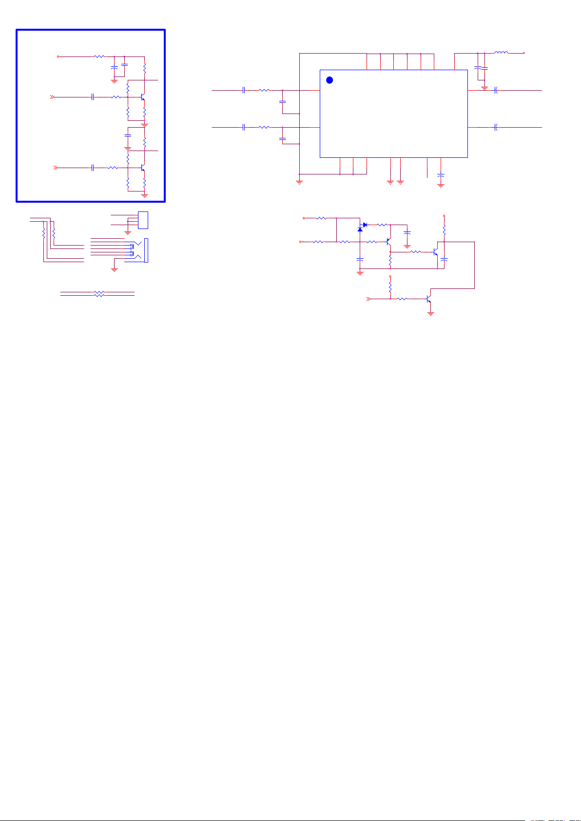
+12V _NO RMAL
AMP _AUO UTR0
AMP _AUO UTR0
AMP _AUO UTL0
AMP _AUO UTL0
R3041K /0603
R3051K/06 03
R-R
1 2
1 2
SP_R +
SP_L +
L-R
PHONE IN =>Specker OFF
PHONE IN =>Specker OFF
PHONE IN =>Specker OFF
PHONE IN =>Specker OFF
SP_L + S P_L
SP_R + S P_R
0/2.2 uF
0/2.2 uF
R90 1 NC/68 R
C90 3
C91 6
SP_R
SP_L +
SP_R +
SP_L
L-R
R-R
R30 7 NC /0 12
R30 8 NC /0 12
For HVDD=12V Load=4ohm
OP_V CC
+
CA900NC /100uF
0/10 K
R91 50/10 K
SP_L
SP_R
R902NC /4.7K
C901NC/0.1 uF
AMP -R
AMP -L
R9030/47 K
R90 6
Q901
1
NC/39 04
2 3
R904NC/47 RR917NC/47 R R 912NC/4.7 K
OP_V CC
C911NC/0. 1uF R9130/47 K
AMP -L
Q902
1
NC/39 04
2 3
R916NC/8. 2K R9 07NC/8.2K
4P/2.5
4
4
3
3
2
2
1
1
CN22
CN29
1
1
5
5
6
6
4
4
7
7
3
3
2
2
HP-JA CK
C30 1 2.2u
AMP -R
C30 0 2.2u
R40 6 1 0K
R40 7 1 0K
AMP -Lin
C918
1nF
AMP -Rin
C920
1nF
+12V _NO RMAL
+5V_ Norma l
1
IN-1
9
IN-2
R32 1
0R
R32 2
NC
16
R32 0
12
PIN 8 Note :
PIN 8 Note :
PIN 8 Note :
PIN 8 Note :
HIGH:OPERATING(8.5V-VCC)
HIGH:OPERATING(8.5V-VCC)
HIGH:OPERATING(8.5V-VCC)
HIGH:OPERATING(8.5V-VCC)
LOW:MUTE(3.3V-6.4V)Ip=40mA
LOW:MUTE(3.3V-6.4V)Ip=40mA
LOW:MUTE(3.3V-6.4V)Ip=40mA
LOW:MUTE(3.3V-6.4V)Ip=40mA
LOW_Standby:(0-2V)Ip<100uA
LOW_Standby:(0-2V)Ip<100uA
LOW_Standby:(0-2V)Ip<100uA
LOW_Standby:(0-2V)Ip<100uA
GND 1818GND 1717GND 16
POWER GND
POWER GND
POWER GND
POWER GND
BAV99
R33 6 1 00
D10 4
3
2
47K
AMP -MUTE
1
1
R34 0 1 00R
+
CA8910 0uF
+5V_ Stand by
AMP -MUTE
5
3 2
GND 5_AMP
22K
GND 1010GND 1111GND 12
PA1517L U 14
Q45
3906
R316
R9204.7K
R92 3 4 .7K
15
GND 2_SIGN AL
2
SIGNAL GND
SIGNAL GND
SIGNAL GND
SIGNAL GND
+
CA9210 0uF
Mute
R31 7 1 K
7
VCC
GND 1313GND 1414GND 15
OUT -1
OUT -2
MUTE/ STAND BY
SVRR
8
3
12
+
CA86100uF
AMP -EN
+12V _NO RMAL
R310
10K
AMP -EN
1
Q19
+
3904
CA9147uF
2 3
AMP -EN
Q904
39041
2 3
L59 0/1206
C7850.1uF
CA95470uF
4
1 2
CA9 0 470u F
+
6
1 2
CA9 4 470u F
+
+12V _NO RMAL
SP_L +
SP_R +
Page 22
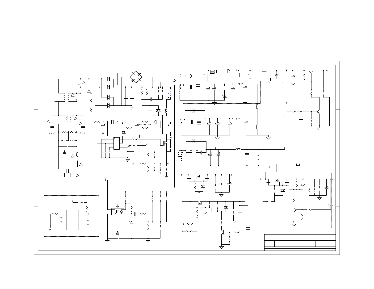
2
NC
NC
BG1
1
3
R137
C39
EC41
R139
R4
R140
R110
1
R111
Q32
R142
R143
R145
R114
C31
R157
1
R159
2 3
R137A
2 3
C38
R146
+5VSB
D+
R138
R136
L13
D17
D18
1 2
1 2
12
C40
23
1
Q31
R141
R147
+12VB
+24VB
R156
R155
R158
12 DB3
12 DB4
3 2
1
2
3 4
IC8
CY3
4
EC11
EC16
Q2
R6
1
Z7
1 2
6
5
VD
C29
100pF
****************
CS
+5VA
R113
1
2
U2
RV1
L2
CON1
L1
1
IC5
1
2
1
2
R2
R12
F1
2
D+
1
2
3
4 5
V
A
L1
R104
CY1
RT1
R13
8
7
VCC
6
VD
D
4
3
N1
4
CY2
C
3
R3
R5
CX1
T3.15AL/250Vac
N L
B
R14
COM
CS
A
1 2 3 4 5 6
1 2DB1
1 2DB2
N1
R108
R109
EC17
R115
3
D1
VCC
R112
C30
COM
P1
4
3
16
T1
1512
3176
C41
2
R144
R208
C45
D16
14
13
11
D19
R132
8
9
R133
10
GATE
+24V
2 3
C42
R148
C43
R149A
R149C
+5VSB +5V
+12VB +12V
D15
R128
R129
C46
R130
R131
Q34
D
G
+12V
Q33
2 3
D
G
R149
R134
4
R135
EC22
EC26
C47
EC34
C48
12
1
R174A
D21
12
1
D22
D20
5
R192A
L14
R209
EC21
1 2
+12VA
EC24
+5VA
EC27
R174
12
C49
R177
R150
Q36
3 2
EC23
EC20
Z9A
L15
EC25
L16
EC35
2A
EC37
R175
1.5A
EC38
1 2
Z8A
R178
1
R151
R192
EC40
R193
EC36
R194
R195
Q35
+24VB +24V
C44
R152
R152A
GATE
Z8
Title
B
Date: 13-Jan-2011 Sheet of
File: E:\MP123-2.1 (2011.01.06)\MP123-2.1 (2011.01.06).ddbDrawn By:
Z9
1 2
2 3
D
G
1
Number RevisionSize
+24VB
+12VB
+33V
PS-ON
+5VSB
0.5A
12
D23
Q35A
C50
MP123
EC40A
R199
2 3
1
R196
R153
Q37
3 2
MEGMEET
654321
Q39
23
R197A
1
R197
1
C50A
R200
12
Z10A
R179
1
R154
GATE
D
R198
Q38
3 2
C
1A
R176
R210R211
EC39
1
B
Z10
1 2
A
1.1
Page 23
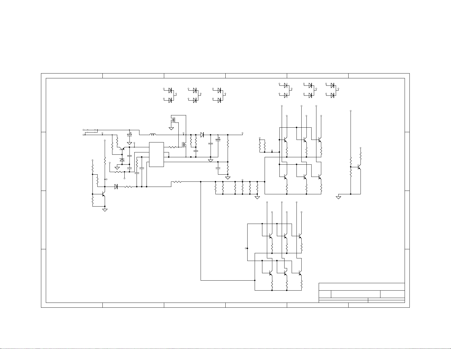
654321
LED9
1
LED1
L5
1 2
1
IC6
2
3
4 5
C26
3
8
7
6
D
J33
+24V
J34
+12V
C
LED
VCC1
R22
ADJ
R1
R59
1
R101
R16
BK/ON
A1
1 2
Q28
3 2
EC2
R15
VCC1
Q1
32
C18
1
Z1
R24
D11
R23
1 2
C24
C27
EN
R74
1
OSP2
2
LED4 LED5
3
23
Q29A
1
R116
1
23
R120
1
Q29
R122
LED2LED3
D25
LED6
D26
1
OSP2 OSP2
2
3
D14
1 2
R117
C32
C34
C36
R170 R171
D27
2
LED+
R160
EC18
R164
LED-
R168
R167
VCC1
R166
R172
1
LED7
3
LED1
1
R163R162
B
1
LED7 LED9
LED10
LED8
D5
1
OSP2 OSP2 OSP2
2
LED10 LED11
3
LED3
LED2
3 2
3 2
LED4
Q5
1
3 2
Q19
1
3 2
LED11
LED12LED8
LED12
D6
LED5
Q14
1
Q20
1
D7
1
2
LED6
Q18
3 2
R182R181R180
Q21
3 2
R184R191R183
2
3
OSP2
EN
R203
R201
Q40
1
R202
3 2
D
C
B
Q22
Q23
1
1
3 2
B
Q25
1
1
A
1 2 3 4 5 6
3 2
Q24
1
3 2
3 2
R187R186R185
Q26
Q27
1
3 2
3 2
R190
R189R188
Title
B
Date: 13-Jan-2011 Sheet of
File: E:\MP123-2.1 (2011.01.06)\MP123-2.1 (2011.01.06).ddbDrawn By:
MEGMEET
Number RevisionSize
MP123
B
A
1.1
2
Page 24
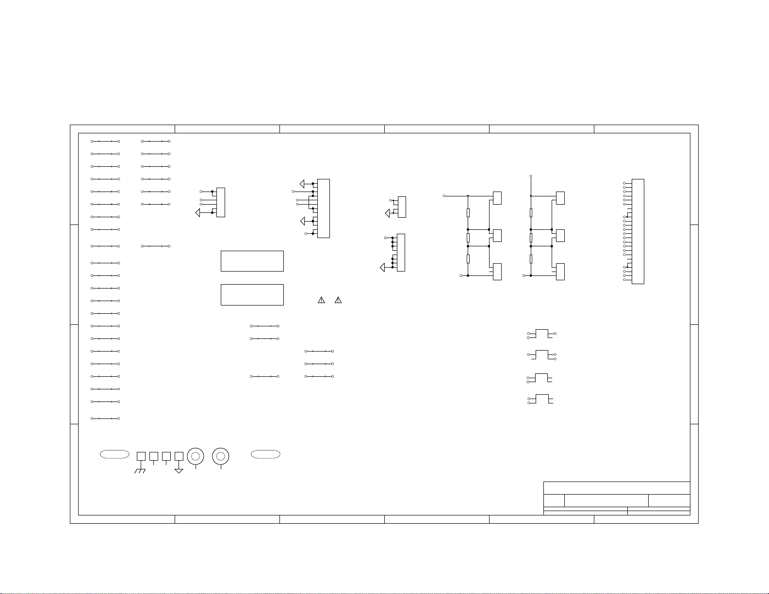
J1
2 2
J2
SGND SGND
J3
D
D+ D+
J4
J5
+12V +12V
J6
J7
J8
4 4
J9
J10
C
J11
VD VD
J12
GATE GATE
J13
SGND SGND
J14
J15
J16
J17
OSP2 OSP2
J18
B
J19
D+ D+
J20
J35
J36
33
OSP2 OSP2
LED+ LED+
D+D+
LED+ LED+
+12V +12V
SGNDSGND
22
+5V +5V
D+D+
+12VB+12VB
+5VSB+5VSB
AA
LED-LED-
OSP2OSP2 +12V +12V
SGNDSGND
SGNDSGND
OSP2OSP2
J21
J22
VCC1VCC1
J23
J24
J25
J26
J29
BK/ON
CON3
1
+12V
2
3
4
ADJ
5
6
1
1.sch
2
2.Sch
+33V +33V
RJ3
RJ4
VCC1 VCC1
RJ7
+5V
PS-ON
+5VSB
+12V
GND GND
654321
LED2
LED4
LED1
LED6
LED3
LED5
LED+
LED+
LED+
LED+
LED11
LED9
LED12
LED7
LED10
LED8
LED+
LED+
LED+
LED+
CON5
1
2
3
4
5
6
7
8
9
10
11
12
13
14
15
16
17
18
19
20
21
22
23
24
D
C
B
LED-
SGND
SGND
LED+
CON6
1
2
R124A
CON7
1
R124
2
R125
CON8
1
2
3
HS1
1
3
1
3
GND
2
GND
1
1
6
GND
4
2
4
HS2
SGND
SGND
HS3
HS4
CON2
1
2
3
4
5
6
7
8
9
10
11
12
13
RJ13
RJ14
SGNDSGND
RJ15
GNDGND
+24V 1
+24V
CON4
2
3
4
CON4A
1
2
3
4
5
6
7
8
LED+
LED-
R126A
R126
R127
CON10
1
2
CON11
1
2
CON12
1
2
3
WARNING1
LABEL
A
FG41FG11FG21FG3
1
1 2 3 4 5 6
M2M1
FG
LABEL
Title
Number RevisionSize
B
Date: 13-Jan-2011 Sheet of
File: E:\MP123-2.1 (2011.01.06)\MP123-2.1 (2011.01.06).ddbDrawn By:
MEGMEET
MP123
A
 Loading...