

ASAHI KASEI AKD5393 User Manual
AKD5393
查询AK5393供应商
ASAHI KASEI [AKD5393 Rev.A]
Evaluation board Rev.A for AK5393
General description
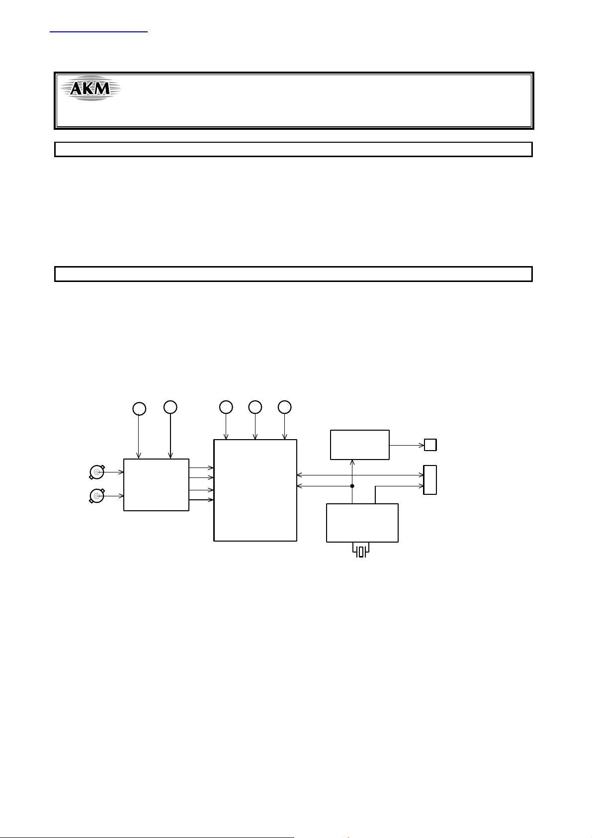
The AKD5393 is an evaluation board for the AK5393 professional audio 24bit A/D converter. The
AKD5393 includes the input buffer circuit and also has a digital interface transmitter. Further, the
AKD5393 can evaluate direct interface with AKM’s DAC evaluation boards.
n
Ordering guide
AKD5393 Rev.A --- Evaluation board for AK5393VS
Function
• On-board Full-differential input buffer circuit
• On-board clock generator
• Compatible with 2 types of interface
1) Direct interface with AKM’s DAC evaluation boards.
2) On-board CS8402 as DIT which transmits optical output.
• A BNC connector for an external clock input.
Lch
Rch
+15V
-15V +3.3V
Input
Buffer
* Circuit diagram and PCB layout are attached at the end of this manual.
+5V GND
CS8402
(DIT)
AK5393
Clock
Generator
Opt Out
D/A Data
10pin Header
<KM059101> ’00/05
- 1 -
ASAHI KASEI [AKD5393 Rev.A]
910
4.7k
n
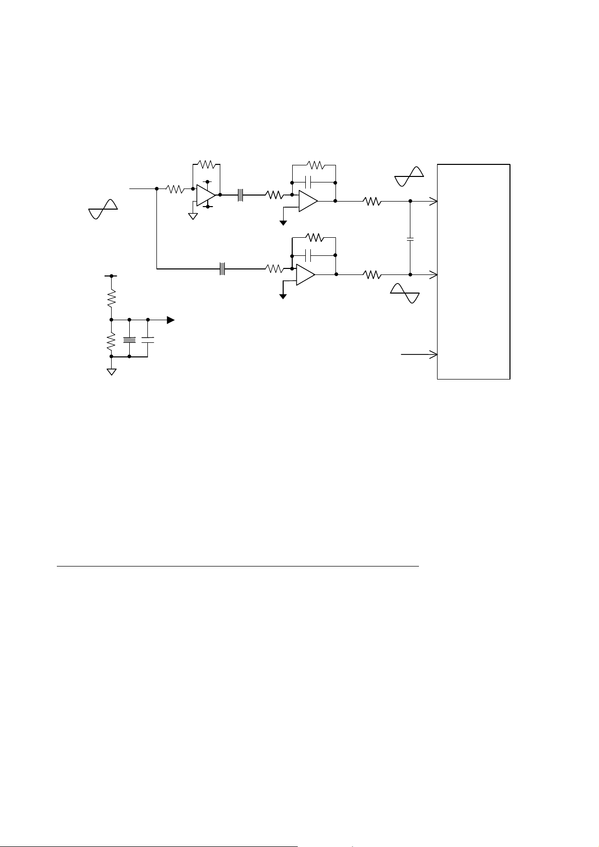
Input buffer circuit
The AKD5393 includes full-differential input buffer circuit with an inverted-amp (gain: -10dB). The capacitor of 10nF
between AIN+ /- decreases the clock feed through noise of modulator, and composes a 1st order LPF (fc=360kHz) with
22ohm resistor before the capacitor. This circuit also has a 1st order LPF (fc=370kHz) composed of op-amp. External
analog signal can be fed through the BNC connector or the Cannon connector.
VP+
+
NJM5532
VA=±5V
VP=±15V
Analog In
VA+
10k
10k
10µ
4.7k
8.1Vpp
Bias
+
0.1µ
Figure 1. Full-differential input buffer circuit example
1: In case of using the BNC connector
[JP2, JP3, JP4, JP5]: Short
[R11, R18]: Open
The resistor value of R10 and R19 should be properly selected in order to much the output
impedance of the signal source.
VP-
47µ
47µ
3k
Bias
3k
Bias
470p
+
910
470p
-
+
"L" at self calibration
22
22
2.45Vpp
2.45Vpp
AK5393
AIN+
10n
AIN-
CAL
ZCAL
2: In case of using the Cannon connector
[JP2, JP3, JP4, JP5]: Open
The resistor value of R10, R11, R18 and R19 should be properly selected in order to much the
output impedance of the signal source.
* AKM assumes no responsibility for the trouble when using the above circuit examples.
n Power supply and Decoupling
VA and VD supplies to the AK5393 are decoupled separately in order to minimize the effect of the digital noise. A system
analog supply is fed to VA. VA and VD lines should be distributed separately from the power unit.
Decoupling capacitors are connected to AK5393 as near as possible, particularly the ceramic capacitor to the VREFL/R
pin.
<KM059101> ’00/05
- 2 -

ASAHI KASEI [AKD5393 Rev.A]
n
Operation sequence
(1) Set up the power supply lines
VP+=+15V, VP- = -15V, VA+=+5V, VD+=+3.3V∼5.25V, AGND=DGND=0V
Each supply line should be distributed from the power unit.
(2) Set up the evaluation modes and jumper pins. (See next item)
There are many jumper pins to cover many evaluation modes.
Please take care of setting.
(3) Set up the DIP SW position for the DIT. (See next item)
This does not affect AK5393 operation.
(4) Power On.
The AK5393 should be reset once by bringing PD "L"(SW4) upon power-up.
(5) AK5393 can be reset by SW4 during operation.
Lower position resets the device, and the upper position is for normal operation.
Note: In any case of changing clocks during operation, the device should be reset by
bringing PD "L". If not followed, the AK5393 may be destroyed since its internal logic
uses dynamic circuit.
n
The evaluation modes and corresponding jumper pin settings.
1. Evaluation Mode
Applicable Evaluation Mode
1-1 Using D/A converter board for the analog performance analysis.
1-2 DIT (Optical Link) [Default]
1-3 All interface signals (MCLK, BICK and LRCK) are fed from external circuit.
1-4 Feed all interface signals to the external circuit through PORT2.
1-1. Using D/A converter board for the analog performance analysis.
The AK5393 can be evaluated by distortion analyzer using various AKM's D/A converter evaluation boards
through PORT2.
[Slave mode]
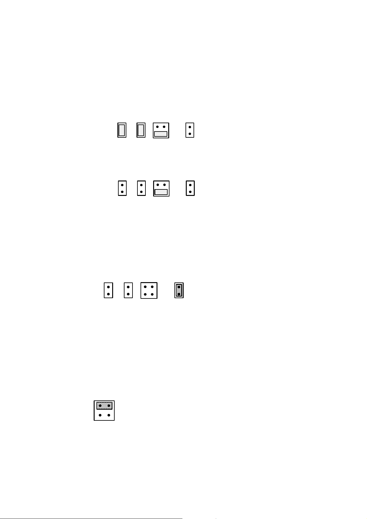
JP9
LR
JP7BCJP11
MCLK
JP12
EXT
XTL
XTE
Figure 2. Jumper set up (D/A)
<KM059101> ’00/05
- 3 -
ASAHI KASEI [AKD5393 Rev.A]
1-2DIT (Optical Link)
PORT1 is used. DIT generates audio Bi-phase signal from received data and which is output through optical
connector (TOTX174). It is possible to connect AKM's D/A converter evaluation boards on the digital-amplifier,
which equips DIR input. There are two kinds of jumper setting depend on the SMODE1 and SMODE2 pin. The
interface signals are output from PORT2. (See the (4)). In case of using external clock through a BNC connector,
select EXT on JP11 (MCLK) and short JP12 (XTE).
[Slave mode] (Default)
JP9
LR
JP7BCJP11
MCLK
JP12
EXT
XTL
XTE
[Master mode]
JP9
LR
JP7BCJP11
MCLK
JP12
EXT
XTL
XTE
Figure 3. Jumper set up (DIT)
1-3 All interface signals (MCLK, BICK and LRCK) are fed from external circuit. [Slave mode]
Under the following setup, MCLK, LRCK and SCLK signals needed for the A/D to operate could be
Fed through PORT2.
J
P9
LR
JP7BCJP11
MCLK
JP12
EXT
XTL
XTE
Figure 4. Jumper set up (EXT)
1-4 Feed all interface signals to the external circuit through PORT2. [Master, Slave mode]
Please set up as same as 1-2. All interfacing signal which drive AK5393 are output through PORT2.
However, the FSYNC signal is input when the position of the SDATA is needed to be controlled.
* Setting for double speed sampling (fs=96kHz)
For the double speed sampling, DFS="L", MCLK=128fs, BICK=64fs(max) are required.
So, when BICK and LRCK are created from 74HC4040 on the board, the crystal oscillator should be changed to
24.576MHz and set JP14 (MCLK2) to 128fs side (see the schematics).
2. BIT CLK (BCF) set up
JP8
128
64
BCF
[JP8] Either 64fs or 128fs for the BCF can be selected. Figure shows 128fs example.
When DFS="H", set JP8 to 64 side.
128: 128fs is fed to AK5393 as BICK.
64: 64fs is fed to AK5393 as BICK.
<KM059101> ’00/05
- 4 -
ASAHI KASEI [AKD5393 Rev.A]
3. Jumper-set up and explanation
Set up the CS8402's data format corresponding the serial data interface of the AK5393.
AKD5393
Data Format
SMODE2
(SW2-5)
SMODE1
(SW2-4)
8402
(SW2-1)
BCF
(JP6)
LRP
(JP10)
Slave mode ON ON ON F H
Mater mode ON OFF OFF R L
I2S Slave mode OFF ON OFF R H
*DIP-SW is ON=”L”
OFF=”H”
I2S master mode OFF OFF OFF R H
Table 1. Serial data interface of AK5393 and CS8402
[SW2-1]: CS8402's data format
ON: MSB justified, 24bit
OFF: IIS Compatible
[JP6]: Define the polarity of SCLK.
F: SCLK is inverted.
R: SCLK coincides with AK5393
[JP10]: Define the polarity of LRCK.
L: LRCK is inverted.
H: LRCK coincides with AK5393.
4. The other function set up
No. PIN ON OFF
*DIP-SW is ON=”L” OFF=”H”
1 8402 See the Table1.
2 DFS 48k 96k
3 HPFE disable enable
4 SM1
Seethe Table 1.
5 SM2
→Selects the sampling rate.
→Selects HPF of AK5393.
→Selects the reference signal for Offset-Cal of K5383
6 CALMODE VCOM AIN
Table 2. DIP-SW2 set-up VCOM:VCOML,VCOMR pin
AIN: Analog input pin (AINL±, AINR±)
[JP13]: Selects the analog power supply source to VA pin of the AK5393.
Open: Supply from the power supply terminal (VA+).
Short: Supply from 3-terminal-voltage regulator (+5V) on the board.
n
The function of the toggle SW.
[SW3] Resets the CS8402. Upper position resets the internal counter of CS8402, then Bi-phase
signal is not output. Keep the "L" position during normal operation.
[SW4] Resets the AK5393. Keep the "H" position during conversion.
<KM059101> ’00/05
- 5 -
ASAHI KASEI [AKD5393 Rev.A]
n
DIP switch set up. (Default is the consumer mode.).
The DIP-SW1 sets the C-bit of CS8402. This set up does not affect the evaluation of the AK5383. In case of using DIT,
need to set it up correctly. For more detailed configurations, please refer to the CS8402
datasheet.
Switch OFF=0,ON=1 Contents
8 PRO = 0 Professional mode, C0=1
7,6 C6 , C7 C6,C7 - Sampling frequency
11
10
01
00
5 C9 C8,C9,C10,C11 - 1bit of channel mode
1
0
4 C1 C1 - Audio mode
1
0
3 TRNPT Transparent mode *CS8402 is CRE
0
1
1,2 EM1,EM0 C2,C3,C4 - Encoded audio signal emphasis
1 1
1 0
0 1
0 0
Table 3. DIP switch set up of CS8402 (Professional mode)
Switch OFF=0,ON=1 Contents
8 PRO = 0 Consumer mode, C0=0 (Default)
7 C2 C2 - Copy
1
Default
6 C3 C3,C4,C5 - Pre-emphasis
Default 1
5 C15 C15 - Generation Status
Default
3,4 FC1, FC0 C24,C25,C26,C27- Sampling frequency
Default
1,2 C8 , C9 C8-C14 - Category code
Default 1 1
0
0
1
0
00
01
10
11
1 0
0 1
0 0
Table 4. DIP switch set up of CS8402 (Consumer mode)
00 - Not indicated. Receiver default to 48kHz.
01 - 48kHz
10 - 44.1kHz
11 - 32kHz
0000 - Mode not indicated. Receiver default to 2-channel mode.
0100 - Stereophonic.
0 - Normal audio
1 - Not audio
Normal mode
Transparent mode
000 - Emphasis not indicated. Receiver defaults to no
emphasis with manual override enable.
100 - None
110 - 50/15usec
111 - CCITT J.17
0 - Copy inhibited
1 - Copy permitted
000 - None
100 - 50/15usec
0 - See the standard
1 - See the standard
0000 - 44.1kHz
0100 - 48kHz
1100 - 32kHz
0000 - 44.1kHz, CD mode
0000000 - General
0100000 - PCM encoder/decoder
1000000 - CD
1100000 - DAT
<KM059101> ’00/05
- 6 -

ASAHI KASEI [AKD5393 Rev.A]
IMPORTANT NOTICE
• These products and their specifications are subject to change without notice. Before considering any use or
application, consult the Asahi Kasei Microsystems Co., Ltd. (AKM) sales office or authorized distributor
concerning their current status.
• AKM assumes no liability for infringement of any patent, intellectual property, or other right in the application or
use of any information contained herein.
• Any export of these products, or devices or systems containing them, may require an export license or other
official approval under the law and regulations of the country of export pertaining to customs and tariffs,
currency exchange, or strategic materials.
• AKM products are neither intended nor authorized for use as critical components in any safety, life support, or
other hazard related device or system, and AKM assumes no responsibility relating to any such use, except
with the express written consent of the Representative Director of AKM. As used here:
(a) A hazard related device or system is one designed or intended for life support or maintenance of safety or
for applications in medicine, aerospace, nuclear energy, or other fields, in which its failure to function or
perform may reasonably be expected to result in loss of life or in significant injury or damage to person or
property.
(b) A critical component is one whose failure to function or perform may reasonably be expected to result,
whether directly or indirectly, in the loss of the safety or effectiveness of the device or system containing it,
and which must therefore meet very high standards of performance and reliability.
• It is the responsibility of the buyer or distributor of an AKM product who distributes, disposes of, or otherwise
places the product with a third party to notify that party in advance of the above content and conditions, and the
buyer or distributor agrees to assume any and all responsibility and liability for and hold AKM harmless from
any and all claims arising from the use of said product in the absence of such notification.
<KM059101> ’00/05
- 7 -
 Loading...