

ASAHI KASEI AKD4393 User Manual
查询AK4393供应商
ASAHI KASEI [AKD4393]
AKD4393
Evaluation board Rev.C for AK4393
General Description
The AKD4393 is an evaluation board for AK4393, which is 96kHz sampling 24Bit ∆Σ DAC. The AKD4393
includes a LPF which can add differential analog outputs from the AK4393 and also has a digital interface with
AKM’s wave generator using ROM data and AKM’s ADC evaluation boards. Therefore, it is easy to evaluate the
AK4393.
<
Ordering Guide
AKD4393 Rev.C --- Evaluation board Rev.C for AK4393: differential output
Function
<
On-board differential output buffer circuit
<
On-board clock generator
<
BNC connector for an external clock input
<
Compatible with 3types of interface
1. Direct interface with evaluation boards for AKM’s A/D converter (AKD539X, AKD535X)
2. Interface with a signal generator (AKD43XX)
3. On-board CS8414 as DIR which accepts optical input.
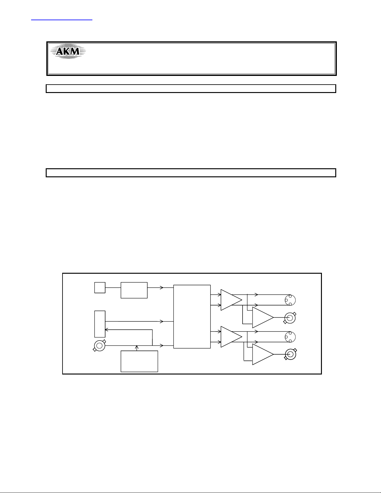
Optical
Input
10pin Header
ROM Data
or
A/D input
Externa l
Clock
C S 8414
(DIR )
Clock
Generator
2nd Order LPF
AK4393
Fig.1 Block diagram
* Circuit diagram and PCB layout are attached at the end of this manual.
Lch
Rch
<KM058804> 1 2000/5
ASAHI KASEI [AKD4393]
<
External Analog Circuit (Rev.C)
The differential output circuit and LPF is implemented on board. The differential outputs of AK4393 is buffered by non-inverted
circuit and output via Cannon connector(differential output). LPF adds differential outputs. NJM5534D is used for op-amp on this
board that has low noise and high voltage torelance characteristics. Analog signal is output via Cannon and BNC connectors on the
board. The output level is about 2.94Vrms(typ@VREF=5.0V) by Cannon and 2Vrms(typ@VREF=5.0V) by BNC.
+15
4.7n
2
3
4.7n
0.1u
4
7
NJM5534D
10u
-15
10u
100
6
Lch
AOUTL-
AOUTL+
47u
47u
560
560
300
300
10n
300
300
10n
10n
10n
300
300
3
2
7
3
2
4
NJM5534D
220
7
4
NJM5534D
220
10u
0.1u
6
10u
0.1u
10u
0.1u
6
10u
0.1u
100
3
2
1
100
430
620
620
430
0.1u
Fig.2 External Analog Filter
<
Operation sequence
1.Set up the jumpers for power supply.
[JP15(REG)] selects power supply for AVDD pin of AK4393.
short: 5V is supplied from regulator. (default)
Nothing should be connected to A5V jack.
open: 5V is supplied from A5V.
2.Set up the power supply lines.
+15V=15V, -15V=-15V: Power supply for op-amp. AVDD of AK4393 is supplied from “+15V” through
regulator (JP15: short).
A5V=5V: This jack is used when AVDD of AK4393 is supplied from this. In this case, JP15
should be open.
DVDD=5V: Power supply for logic circuit on this board.
VP=3V∼5.25V: Digital (set JP10 to VP),
AGND=DGND=0V .
Each supply line should be distributed from the power unit.
3.Set up the evaluation modes by jumper pins and DIP switches.(See next item.)
4.Power on.(The AK4393 should be reset once by bringing PD "L" upon power-up.)
*SW1 resets the AK4393 during operation.
The AK4393 is reset at SW1="L" and exits resetting at SW1="H".
<KM058804> 2 2000/5
ASAHI KASEI [AKD4393]
<
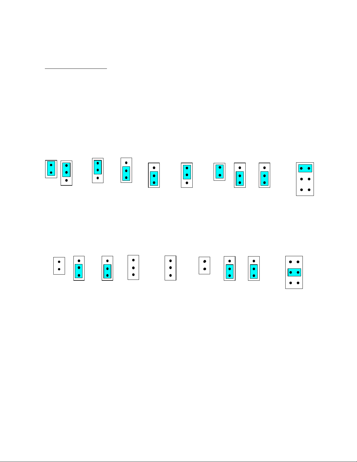
The evaluation modes and corresponding jumper pins setting
1. Evaluation Modes
•
Applicable Evaluation Mode
(1) DIR(Optical Link)
(2) Ideal sine wave generated by ROM data
(3) Using AD converted data
(4)All interface signals including master clock are fed externally.
(1) DIR(Optical Link) (default)
PORT2 is used for the evaluation using such as CD test disk. The DIR generates MCLK, BICK and LRCK SDATAfrom
the received data through optical connector(PORT2: TORX176).
BCP
JP4
INV
THR
BCP
(others)(MSB
INV
THR
JP5
BI
XTL/EXT
DIR
JP6
LR
DIR
XTL/EXT
JP7
SD
JP8
CKDIV1
2X
1X
JP14
1/2X
1X
CKDIV2
JP9
DIR
XTL
EXT
CLK
JP1
JP2
VDD
GND
CS8414
justified)
Fig.3 Jumper set-up (DIR)
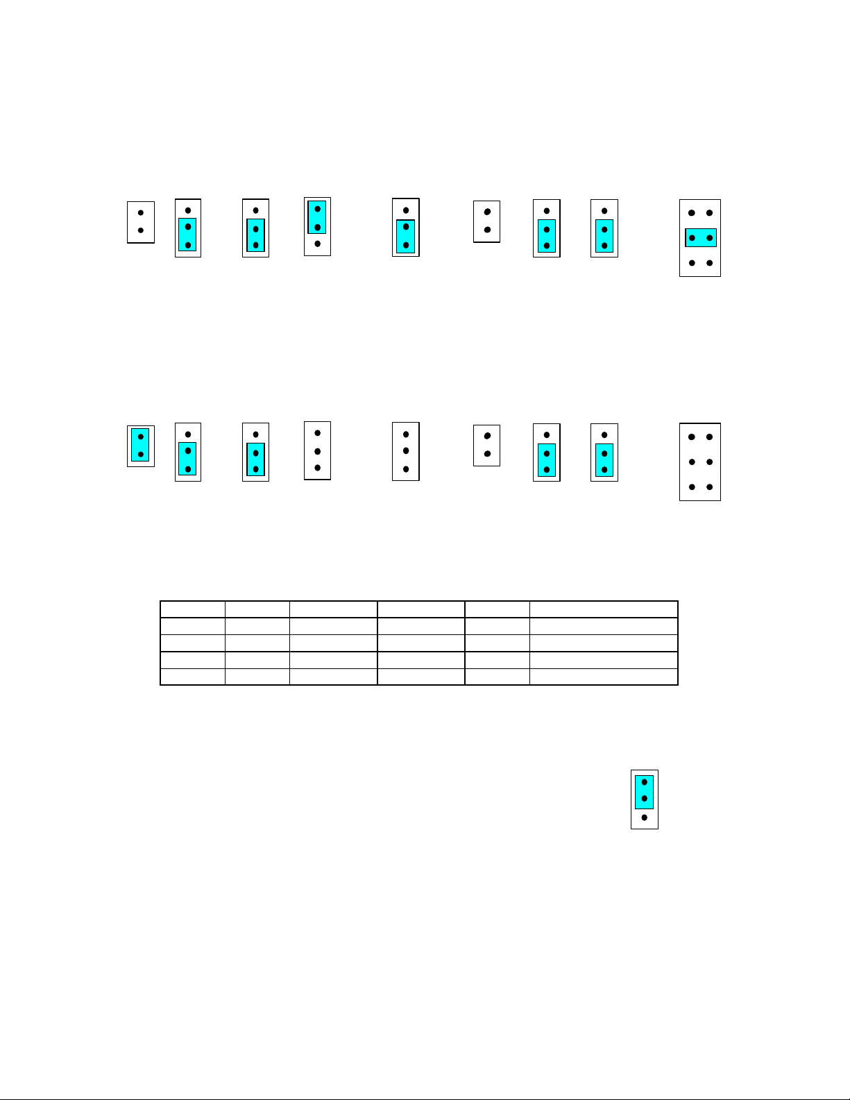
(2) Ideal sine wave generated by ROM data
Digital signal generated by AKD43XX are used. PORT1 is used for the interface with AKD43XX. Master clock is sent
from AKD4393 to AKD43XX then LRCK, BICK and SDATA are sent from AKD43XX to AKD4393.
JP1
JP2
C S8414
VDD
GND
JP4
BCP
INV
THR
JP5
XTL/EXT
DIR
BI
JP6
LR
DIR
XTL/EXT
JP7
SD
JP8
CKDIV 1
2X
1X
JP14
1/2X
1X
CKDIV2
JP9
DIR
XTL
EXT
CLK
Fig.4 Jumper set-up (ROM data)
<KM058804> 3 2000/5
ASAHI KASEI [AKD4393]
(3) Using AD converted data
AD converted data from AKM’s AD evaluation boards(AKD539X, AKD535X) is used through PORT1.
* In case of using external clock through a BNC connector, select EXT of JP9 and short JP1.
* In case of using the double speed sampling mode, select 1/2X of JP8 and set S2-2(DFS) on.
JP1
JP2
C S8414
VDD
GND
JP4
BCP
INV
THR
JP5
XTL/EXT
DIR
BI
JP6
LR
DIR
XTL/EXT
JP7
SD
JP8
CKDIV 1
2X
1X
JP14
1/2X
1X
CKDIV2
DIR
XTL
EXT
Fig.5 Jumper set-up (A/D)
(3) All interface signals including master clock are fed externally.
Under the following set-up, MCLK, LRCK and SCLK signals needed for the D/A to operate could be fed through PORT1.
JP1
JP2
C S8414
VDD
GND
JP4
BCP
INV
THR
JP5
XTL/EXT
DIR
BI
JP6
LR
DIR
XTL/EXT
JP7
SD
JP8
CKDIV 1
2X
1X
JP14
1/2X
1X
CKDIV2
DIR
XTL
EXT
Fig.6 Jumper set-up (ext.)
2. MCLK set-up
When the LRCK is fed from the 74HC4040 on the board, The ratio of MCLK to LRCK can be selected by JP8 and JP14.
JP14 JP8 X'tal MCLK fs MCLK/LRCK
1X 1X 12.288MHz 12.288MHz 48kHz 256
1X 2X 24.576MHz 24.576MHz 48kHz 512
1/2X 1X 24.576MHz 12.288MHz 96kHz 128
1/2X 2X 49.152MHz 12.288MHz 96kHz 128
Table.1 set-up example
JP9
CLK
JP9
CLK
3. BICK set-up
JP3
When BICK is supplied from U1(74HC4040), either 32fs or 64fs could be
selected. Fig.8 shows 64fs mode. 64fs mode is recommended.
*Only mode 0(LSB justified 16bit mode) can correspond to 32fs.
64
32
BCS
Fig.7 Jumper Set-up (BCS)
<KM058804> 4 2000/5
ASAHI KASEI [AKD4393]
4. DIP switch set-up
Confirm the set-up of the DIP switch before the operation. “ON” means “H” and “OFF” means “L”.
4-1. Set-up of SW3, SW4(Mode set-up of AK4393: see the data sheet of AK4393)
DIF2 DIF1 DIF0 Mode BICK
OFF OFF OFF 0: LSB justified, 16bit
OFF OFF ON 1: LSB justified, 20bit
OFF ON OFF 2: LSB justified, 24bit
OFF ON ON 3: I2S
ON OFF OFF 4: MSB justified, 24bit
≥32fs
≥40fs
≥48fs
≥48fs
≥48fs
(default)
Table 2 Audio Serial Interface Format Select Pins (SW3-5,6,7)
4-2. Set-up of SW6 (Mode set-up of CS8414. About details, see the data-sheet of CS8414)
Adjust the audio data format of CS8414 (DIR) to AK4393. CS8414 does not match the LSB justified 20bit/24bit mode of
AK4393.
M3
(SW6-2)M2(SW6-3)M1(SW6-4)M0(SW6-5)
OFF OFF OFF OFF MSB justified, 24bit INV
OFF OFF ON OFF I2S THR (default)
OFF ON OFF ON LSB justified, 16bit THR
SW6-1 (SEL): Usually ON.
SW6-6 (CS12): Select the channel for indicating the channel status.
ON: Rch (default), OFF: Lch
5. Parallel/Serial Control
SW5: set up P/S pin of AK4393.
H: parallel mode. PORT3 is used JP11, 12 and 13 should be open.
L: serial mode. PORT3 is used. JP11, 12 and 13 should be open.
6. Other set-up
SW1: Reset of AK4393. Select "H" during operation.
SW2: Soft-mute of AK4393. The soft-mute is executed during SW2 pushed.
LE1 : This LED shows pre-emphasis status. It turns on when the data is pre-emphasized.
LE2 : This LED shows the output of VERF pin in CS8414. It turns on when the error is occured in CS8414.
Data format JP4
Table 3. Set-up of SW6
<KM058804> 5 2000/5

ASAHI KASEI [AKD4393]
<
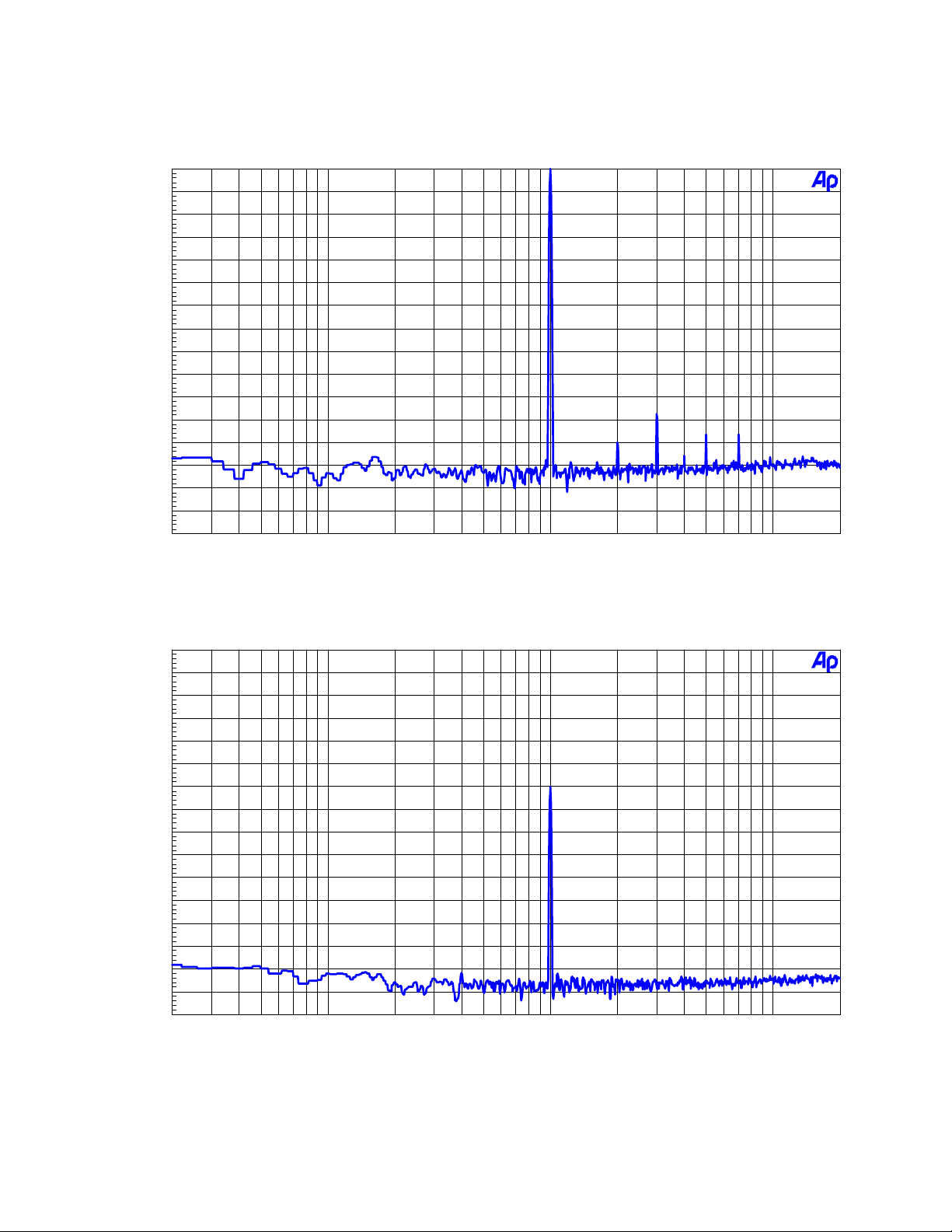
AK4393 Measurement Example
Conditions:
AVDD =DVDD= 5.0V
Interface = DIR (44.1kHz, 96kHz)
MCLK = 256fs(fs=44.1kHz, 96kHz)
BICK = 64fs
fs = 44.1kHz, 96kHz
Input data = 24bit
Measurement unit: Audio Precision System Two Cascade (fs=44.1kHz, 96kHz)
(AKD4393 Rev.C: differential output)
fs Result
44.1kHz
THD+N 102.3 20kLPF
DR 120.0 22kLPF + A-weighted
S/N 119.9 22kLPF + A-weighted
96kHz
THD+N 100.9 40kLPF
DR 119.5 80kLPF + A-weighted
S/N 119.7 80kLPF + A-weighted
Plot
FFT Point: 16384
Window: Equiripple
Averages: 4
<KM058804> 6 2000/5
ASAHI KASEI [AKD4393]
(fs=44.1kHz)
AKM AK4393 FFT (Input Leve=0dBFS,fin=1kHz)
+0
-10
-20
-30
-40
-50
-60
d
-70
B
-80
r
-90
A
-100
-110
-120
-130
-140
-150
-160
20 20k50 100 200 500 1k 2k 5k 10k
Hz
FFT (Input Level=0dBFS, fin=1kHz)
AKM AK4393 FFT (Input Leve=-60dBFS,fin=1kHz)
+0
-10
-20
-30
-40
-50
-60
d
-70
B
-80
r
-90
A
-100
-110
-120
-130
-140
-150
-160
20 20k50 100 200 500 1k 2k 5k 10k
Hz
FFT (Input Level=-60dBFS, fin=1kHz)
<KM058804> 7 2000/5
 Loading...