

ASAHI KASEI AK4524 User Manual
查询AK4524VF供应商
ASAHI KASE I [AK4524]
AK4524
24Bit 96kHz Audio CODEC
GENERAL DESCRIPTIO N
The AK4524 is a high performance 24bit CODEC for the 96kHz recording system. The ADC has an
Enhanced Dual Bit architecture with wide dynamic range. The DAC uses the new developed Advanced
Multi Bit architecture and achieves low outband noise and high jitter tolerance by use of SCF (switched
capacitor filter) techniques. The AK4524 has an input PGA and is well suited MD, DVTR system and
musical instruments.
FEATURES
· 24bit 2ch ADC
- 64x Oversampling
- Single-End Inputs
- S/(N+D): 90dB
- Dynamic Range, S/N: 100dB
- Digital HPF for offset cancellation
- Input PGA with +18dB gain & 0.5dB step
- Input DATT with -72dB att
- I/F format: MSB justified or I
· 24bit 2ch DAC
- 128x Oversampling
- 24bit 8 times Digital Filter
Ripple: ±0.005dB, Attenuation: 75dB
- SCF
- Differential Outputs
- S/(N+D): 94dB
- Dynamic Range, S/N: 110dB
- De-emphasis for 32kHz, 44.1kHz, 48kHz sampling
- Output DATT with -72dB at t
- Soft Mute
- I/F format: MSB justified, LSB justified or I
· High Jitter Tolerance
· 3-wire Serial Interface for Volume Control
· Master Clock
- X’tal Oscillating Circuit
- 256fs/384fs/512fs/768fs/1024fs
· Master Mode/Slave Mode
· 5V operation
· 3V Power Supply Pin for 3V I/F
· Small 28pin VSOP package
2
S
2
S
M0050-E-01 1999/5
- 1 -
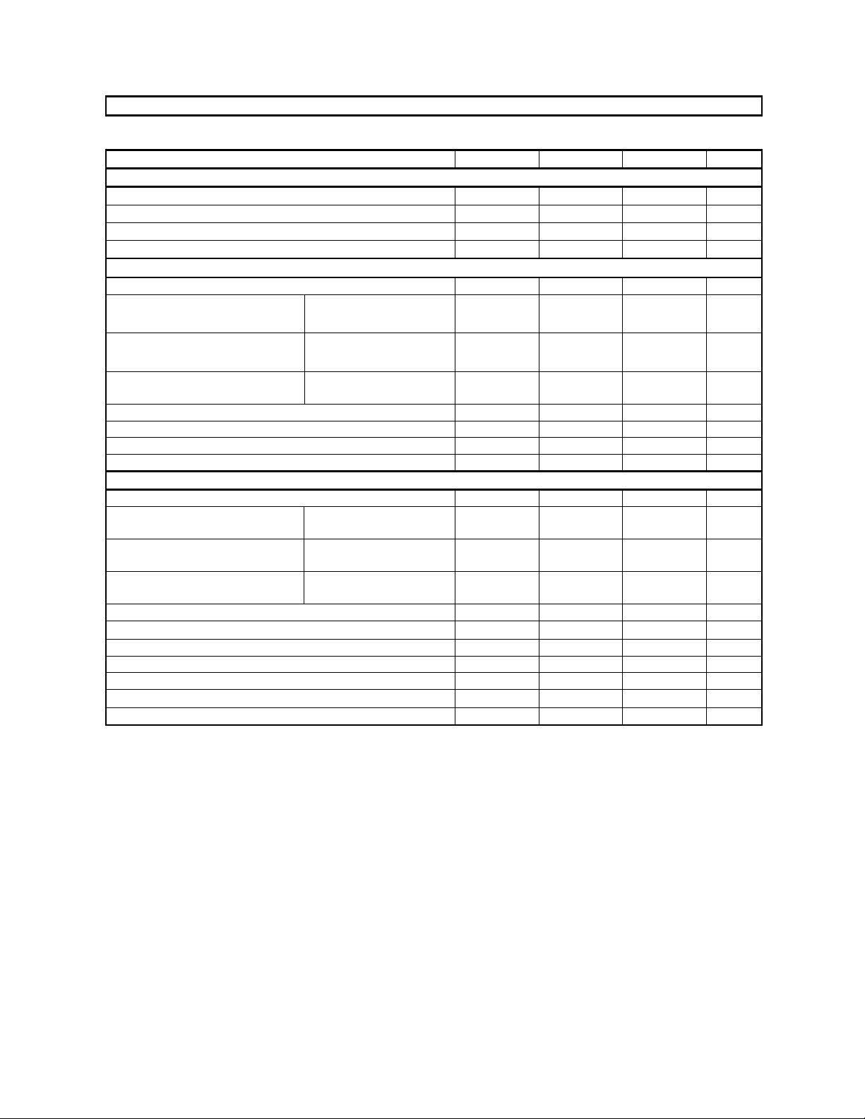
ASAHI KASE I [AK4524]
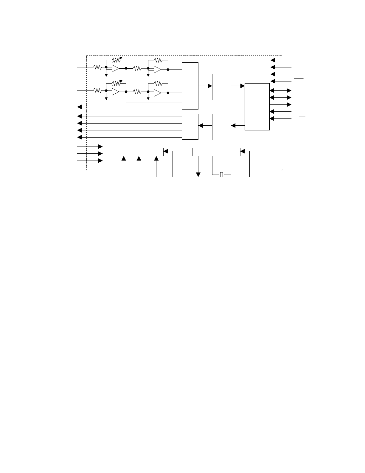
n Block Diagram
VD
AINL
AINR
VCOM
AOUTL+
AOUTLAOUTR+
AOUTR-
VREF
VA
AGND
ADC
DAC
Control Register I/F Clock Gen. & Divider
CS CCLK CDTI CIF CLKO XTO XTI XTALE
HPF
DATT
Audio I/F
Controller
DATT
SMUTE
VT
DGND
PD
LRCK
BICK
SDTO
SDTI
M/ S
Block Diagram
M0050-E-01 1999/5
- 2 -
ASAHI KASE I [AK4524]
n Ordering Guide
AK4524VF -10~+70°C 28pin VSOP (0.65mm pitch)
AKD4524 Evaluation Board
n Pin Layout
VCOM
AINR
AINL
VREF
AGND
VA
(Internal pull down) TEST
XTO
XTI
XTALE
LRCK
BICK
SDTO
1
2
3
4
5
6
7
8
9
10
11
12
13
AK4524
Top
View
28
27
26
25
24
23
22
21
20
19
18
17
16
AOUTR+
AOUTR-
AOUTL+
AOUTL-
DGND
VD
VT
CLKO
M/ S
PD
CIF
CS
CCLK
SDTI CDTI
14 15
M0050-E-01 1999/5
- 3 -
ASAHI KASE I [AK4524]
PIN/FUNCTION
No. Pin Name I/O Function
1VCOM O
2 AINR I Rch Analog Input Pin
3 AINL I Lch Analog Input Pin
4VREF I
5 AGND - Analog Ground P i n
6 VA - Analog Power Supply Pin, 4.75 ~ 5.25V
7 TEST I T est Pin (Internal pull-down pin)
8XTO OX’tal Output Pin
9 XTI I X’tal/Master Clock Input Pin
10 XTALE I
11 LRCK I/O Input/Output Channel Clock Pi n
12 BICK I/O Audio Serial Data Clock Pin
13 SDTO O Audio Serial Data Output Pin
14 SDTI I Audio Serial Data Input Pin
15 CDTI I Control Data Input Pin
16 CCLK I Control Data Clock Pin
17 CS I Chip Select Pin
18 CIF I
19 PD I
20 M/ S I
21 CLKO O Master Clock Output Pin
22 VT - Output Buffer Power Supply Pin, 2.7 ~ 5.25V
23 VD - Digital Power Supply Pin, 4.75 ~ 5.25V
24 DGND - Digital Ground Pin
25 AOUTL- O Lch Negative Analog Output Pin
26 AOUTL+ O Lch Positive Analog Output Pin
27 AOUTR- O Rch Negative Analog Output Pin
28 AOUTR+ O Rch Positive Analog Output Pin
Common Voltage Output Pin, VA/2
Bias voltage of ADC inputs and DAC outputs.
Voltage Reference Input Pin, VA
Used as a voltage reference by ADC & DAC. VREF is connected externally to
filtered VA.
X’tal Osc Enable Pin
“H”: Enable, “L”: Disable
Control Data I/F Format Pin
“H”: CS falling trigger, “L”: CS rising trigger
Power-Down M ode Pin
“H”: Power up, “L”: Power down, reset and initialize the control register.
Master/Slave Mode Pin
“H”: Master mode, “L”: Slave mode
Note: All input pins except pull-down pins should not be left floating.
M0050-E-01 1999/5
- 4 -

ASAHI KASE I [AK4524]
ABSOLUTE MAXI MUM RATINGS
(AGND, DGND=0V; Note 1)
Parameter Symbol min max Units
Power Supplies: Analog
Digital
Output Buffer
VD-VA
Input Current, Any Pin Except Supplies IIN Analog Input Voltage VINA -0.3 VA+0.3 V
Digital Input Voltage VIND -0.3 VA+0.3 V
Ambient Temperature (powered applied) Ta -10 70
Storage Temperature Tstg -65 150
Note:1. All voltages with respect to ground.
WARNING: Operation at or beyond these limits may result in permanent damage to the device.
Normal operation is not guaranteed at these extremes.
VA
VD
VT
VDA
-0.3
-0.3
-0.3
-
6.0
6.0
6.0
0.3
10 mA
±
V
V
V
V
C
°
C
°
RECOMMENDED OPERATING CONDITIONS
(AGND, DGND=0V; Note 1)
Parameter Symbol min typ max Units
Power Supplies
(Note 2)
Voltage Reference VREF 3.0 - VA V
Analog
Digital
Output Buffer
VA
VD
VT
4.75
4.75
2.7
5.0
5.0
3.0
5.25
VA
VD
V
V
V
Note:1. All voltages with respect to ground.
2. VA and VD should be powered at the same time or VA should be powered earlier than VD.
The power up sequence between VA and VT, or VD and VT is not critical.
*AKM assumes no responsibility for the usage beyond the conditions in this datasheet.
M0050-E-01 1999/5
- 5 -
ASAHI KASE I [AK4524]
ANALOG CHARA CTERISTICS
(Ta=25°C; VA, VD, VT=5.0V; AGND=DGND=0V; VREF=VA; fs=44.1kHz; Signal Frequency =1kHz; 24bit Data;
Measurement frequency = 10Hz ~ 20kHz at fs=44.1kHz, 10Hz ~ 40kHz at fs=96kHz; unless otherwise specified)
Parameter min typ max Units
Input PGA Characteristics:
Input Voltage (Note 3) 2.7 2.9 3.1 Vpp
Input Resistance 5 10 15 k
Step Size 0.2 0.5 0.8 dB
Gain Control Range 0 18 dB
ADC Analog Input Characteristics: IPGA=0dB
Resolution 24 Bits
S/(N+D) (-0.5dBFS) fs=44.1kHz
fs=96kHz
DR (-60dBFS) fs=44.1kHz, A-weighted
fs=96kHz
S/N fs=44.1kHz, A-weighted
fs=96kHz
Interchannel Isolation 90 105 dB
Interchannel Gain Mismatch 0.2 0.5 dB
Gain Drift 20 - ppm/°C
Power Supply Rejection (Note 4) 50 - dB
DAC Analog Output Characteristics:
Resolution 24 Bits
S/(N+D) (0dBFS) fs=44.1kHz
fs=96kHz
DR (-60dBFS) fs=44.1kHz, A-weighted
fs=96kHz
S/N fs=44.1kHz, A-weighted
fs=96kHz
Interchannel Isolation 100 110 dB
Interchannel Gain Mismatch 0.2 0.5 dB
Gain Drift 20 - ppm/°C
Output Voltage (Note 5) 5.0 5.4 5.8 Vpp
Load Resistance (In case of AC load) 1 k
Output Current (In case of AC load) 1.5 mA
Load Capacitance 25 pF
84
80
94
88
94
88
88
85
104
96
104
96
90
88
100
96
100
96
94
93
110
104
110
104
W
dB
dB
dB
dB
dB
dB
dB
dB
dB
dB
dB
dB
W
Note: 3. Full scale (0dB) of the input voltage at PGA=0dB.
This voltage is proportional to VREF. Vin=0.58 x VREF.
4. PSR is applied to VA, VD, VT with 1kHz, 50mVpp. VREF pin is held a constant voltage.
5. Full scale (0dB) of the output voltage when summing the differential outputs, AOUT+/- by unity gain.
This voltage is proportional to VREF. Vout=1.08 x VREF x Gain.
M0050-E-01 1999/5
- 6 -
ASAHI KASE I [AK4524]
Parameter min typ max Units
Power Supplies
Power Supply Current
Normal Operation ( PD
VA
VD+VT (fs=44.1kHz)
(fs=96kHz)
Power-down mode ( PD
VA
VD+VT
Note: 6. XTALE=”L” and all digital input pins are held VD or DGND.
= “H”)
= “L”) (Note 6)
30
16
24
10
10
45
24
36
100
100
mA
mA
mA
uA
uA
FILTER CHARACTERISTICS
(Ta=25°C; VA, VD=4.75 ~ 5.25V; VT=2.7 ~ 5.25V; fs=44.1kHz; DEM=OFF)
Parameter Symbol min typ max Units
ADC Digital Filter (Decimation LPF):
Passband (Note 7) -0.005dB
-0.02dB
-0.06dB
-6.0dB
Stopband SB 24.34 kHz
Passband Ripple PR
Stopband Attenuation SA 80 dB
Group Delay (Note 8) GD 31 1/fs
Group Delay Distortion
ADC Digital Filter (HPF):
Frequency Respons e (Note 5) -3dB
-0.5dB
-0.1dB
DAC Digital Filter:
Passband (Note 7) -0.01dB
-6.0dB
Stopband SB 24.1 kHz
Passband Ripple PR
Stopband Attenuation SA 75 dB
Group Delay (Note 8) GD 30 1/fs
DAC Digital Filter + SCF:
Frequency Response:
0 ~ 20.0kHz
~ 40kHz (Note 9)
PB 0
-
-
-
GD 0 us
D
FR 0.9
PB 0
- 22.05
FR
20.02
22.20
22.05
2.7
6.0
0.2
±
0.3
±
19.76
-
-
-
0.005 dB
±
20.0
-
0.005 dB
±
kHz
kHz
kHz
kHz
Hz
Hz
Hz
kHz
kHz
dB
dB
Note: 7. The passband and stopband frequencies scale with fs. For example, 20.02kHz at -0.02dB is 0.454 x fs.
The reference frequency of these responses is 1kHz.
8. The calculating delay time which occurred by digital filtering. This time is from the input of analog signal to
setting the 24bit data of both channels to the output register for ADC.
For DAC, this time is from setting the 24bit data of both channels on input register to the output of analog
signal.
9. fs=96kHz.
M0050-E-01 1999/5
- 7 -
ASAHI KASE I [AK4524]
DIGITAL CHARACTERISTICS
(Ta=25°C; VA, VD=4.75 ~ 5.25V; VT=2.7 ~ 5.25V)
Parameter Symbol min typ Max Units
High-Level Input Voltage
Low-Level Input Voltage
High-Level Output Voltage (Iout=-100uA) (Note 10)
Low-Level Output Voltage (Iout=100uA)
Input Leakage Current Iin - -
VIH
VIL
VOH
VOL
2.2
-
2.7 / VT-0.5
-
-
-
-
-
-
0.8
-
0.5
10 uA
±
V
V
V
V
Note: 10. Min value is lower voltage of 2.7V or VT-0.4V.
SWITCHING CHARACTERISTICS
(Ta=25°C; VA, VD=4.75 ~ 5.25V, VT=2.7 ~ 5.25V; CL=20pF)
Parameter Symbol min typ max Units
Master Clock Timing
Crystal Resonator Frequency 11.2896 24.576 MHz
External Clock Frequency
CLKO Output
(X’tal mode)
Pulse Width Low
Pulse Width High
Frequency
Duty Cycle
fCLK
tCLKL
tCLKH
fMCK
dMCK
8.192
0.4/fCLK
0.4/fCLK
11.2896
35
49.152 MHz
ns
ns
24.576
65
MHz
%
LRCK Frequency
Normal Speed Mode (DFS0=”0”, DFS1=”0”)
Double Speed Mode (DFS0=”1”, DFS1=”0”)
Quad Speed Mode (DFS0=”0”, DFS1=”1”)
Duty Cycle Slave mode
Master mode
fsn
fsd
fsq
32
64
128
45
48
96
192
55 %
50
kHz
kHz
kHz
%
Audio Interface Timing
Slave mode
BICK Period
BICK Pulse Width Low
Pulse Width High
LRCK Edge to BICK “” (Note 11)
BICK “” to LRCK Edge (Note 11)
2
LRCK to SDTO (MSB) (Except I
S mode)
BICK “¯” to SDTO
SDTI Hold Time
SDTI Setup Time
tBCK
tBCKL
tBCKH
tLRB
tBLR
tLRS
tBSD
tSDH
tSDS
81
33
33
20
20
40
40
20
20
ns
ns
ns
ns
ns
ns
ns
ns
ns
Master mode
BICK Frequency
BICK Duty
BICK “¯” to LRCK
BICK “¯” to SDTO
SDTI Hold Time
SDTI Setup Time
fBCK
dBCK
tMBLR
tBSD
tSDH
tSDS
-20
-20
20
20
64fs
50
20
20
Hz
%
ns
ns
ns
ns
Note 11. BICK rising edge must not occur at the same time as LRCK edge.
M0050-E-01 1999/5
- 8 -
ASAHI KASE I [AK4524]
Parameter Symbol min typ max Units
Control Interface Timing
CIF=”0”
CCLK Period
CCLK Pulse Width Low
Pulse Width High
CDTI Setup Time
CDTI Hold Time
CS “H” Time
CS “L” Time
CS “” to CCLK “”
CCLK “” to CS “”
tCCK
tCCKL
tCCKH
tCDS
tCDH
tCSW
tCSW
tCSS
tCSH
200
80
80
40
40
150
150
150
50
ns
ns
ns
ns
ns
ns
ns
ns
ns
CIF=”1”
CCLK Period
CCLK Pulse Width Low
Pulse Width High
CDTI Setup Time
CDTI Hold Time
CS “H” Time
CS “L” Time
CS “¯” to CCLK “”
CCLK “” to CS “¯”
tCCK
tCCKL
tCCKH
tCDS
tCDH
tCSW
tCSW
tCSS
tCSH
200
80
80
40
40
150
150
150
50
ns
ns
ns
ns
ns
ns
ns
ns
ns
Reset Timing
PD
Pulse Width (Note 12)
RSTAD “” to SDTO valid (Note 13)
tPD
tPDV
150
516
ns
1/fs
Note:12. The AK4524 can be reset by bringing PD “L”.
13. These cycles are the number of LRCK rising from RSTAD bit.
M0050-E-01 1999/5
- 9 -
ASAHI KASE I [AK4524]
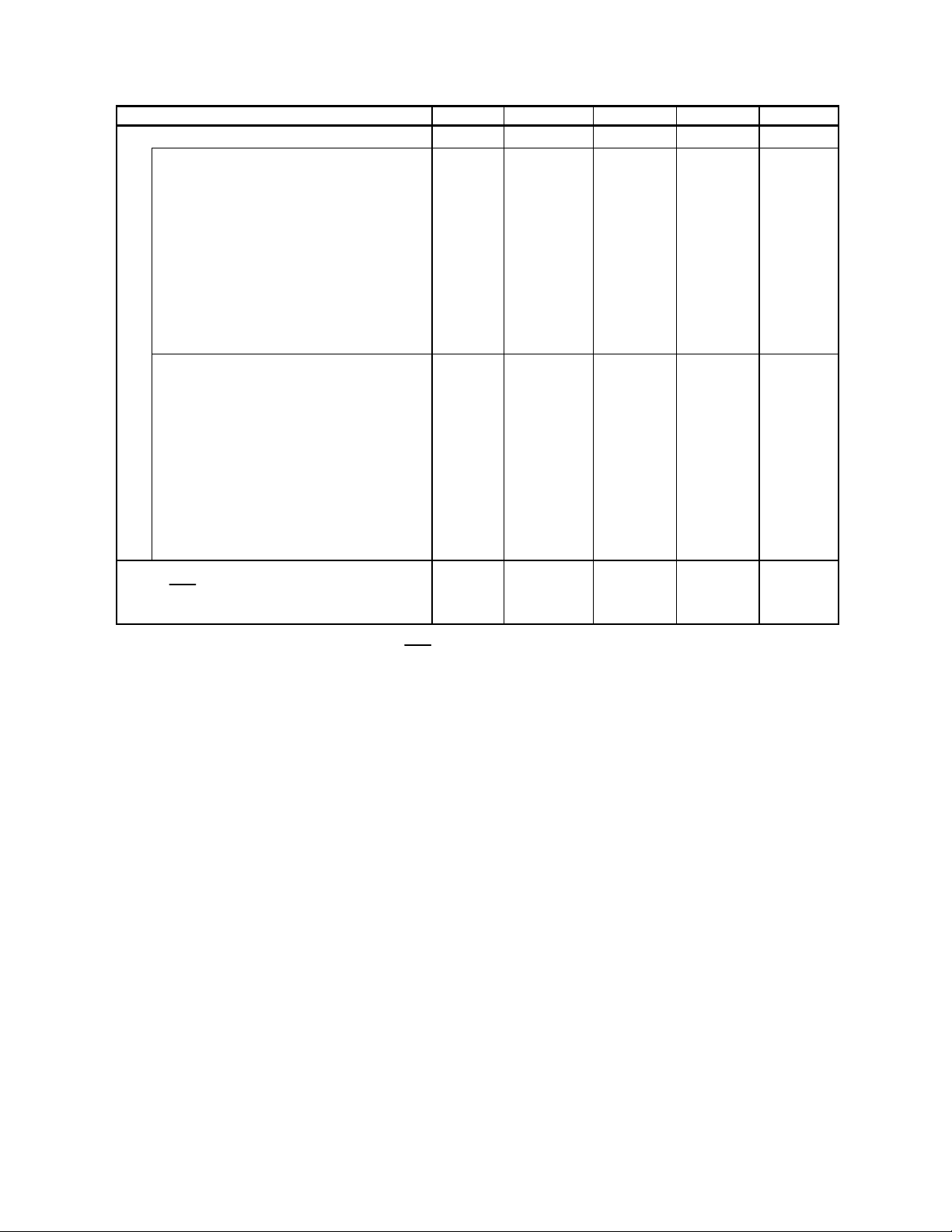
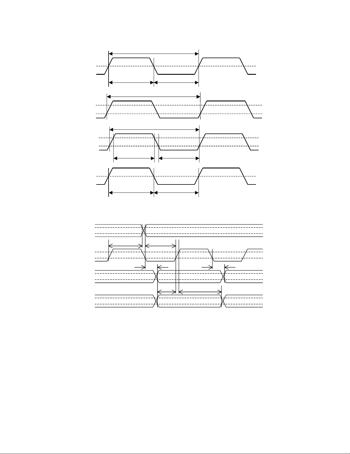
n Timing Diagram
1/fCLK
MCLK
LRCK
BICK
CLKO
LRCK
tCLKH
1/fs
tBCK
tBCKH
tH
dMCK=tH/(tH+tL) or tL/(tH+tL)
Clock Timing
tBLR tLRB
1.5V
tCLKL
VIH
VIL
VIH
VIL
tBCKL
1.5V
tL
VIH
VIL
BICK
SDTO
SDTI
tLRS tBSD
tSDS
Audio Interface Timing (Slave mode)
tSDH
VIH
VIL
VIH
VIL
VIH
VIL
M0050-E-01 1999/5
- 10 -
 Loading...