

ASAHI KASEI AK4386 User Manual

Audio
DIF1
8X
De-emphasis
Control
Clock
DFS1
DFS0
8X
DIF0
∆Σ
DAC
AK4386
查询AK4386供应商
ASAHI KASEI [AK4386]
The AK4386 is a 24bit low voltage & low power stereo DAC. The AK4386 uses the Advanced Multi-Bit ∆Σ
architecture, this architecture achieves DR=100dB at 3V operation. The AK4386 integrates a
combination of SCF and CTF filters increasing performance for systems with excessive clock jitter. The
AK4386 is suitable for the portable audio system like MP3 and the home audio systems like STB and TV,
etc as low power and small package. The AK4386 is offered in a space saving 16pin TSSOP package.
100dB 96kHz 24-Bit 2ch
GENERAL DESCRIPTION
FEATURES
o Sampling Rate: 8kHz ∼ 96kHz
o 24-Bit 8 times FIR Digital Filter
o SCF with high tolerance to clock jitter
o Single-ended output buffer
o Digital de-emphasis for 44.1kHz sampling
o I/F Format: 24-Bit MSB justified, 16/24-Bit LSB justified, I2S Compatible
o Master Clock:
512/768/1024/1536fs for Half Speed (8kHz
256/384/512/768fs for Normal Speed (8kHz ∼ 48kHz)
128/192/256/384fs for Double Speed (48kHz ∼ 96kHz)
o CMOS Input Level
o THD+N: −86dB
o DR, S/N: 100dB(@VDD=3.0V)
o Power Supply: 2.2 to 3.6V
o Ta = −40 ∼ 85°C
o 16pin TSSOP
PDN
DEM TEST
MCLK
Divider
∼ 24kHz)
VDD
VSS
VCOM
LRCK
BICK
SDTI
Data
Interface
Interpolator
Interpolator
∆Σ
Modulator
∆Σ
Modulator
SCF
CTF
SCF
CTF
LOUT
ROUT
MS0280-E-00 2003/12
- 1 -
ASAHI KASEI [AK4386]
n Ordering Guide
AK4386VT −40 ∼ +85°C 16pin TSSOP (0.65mm pitch)
AKD4386 Evaluation Board for AK4386
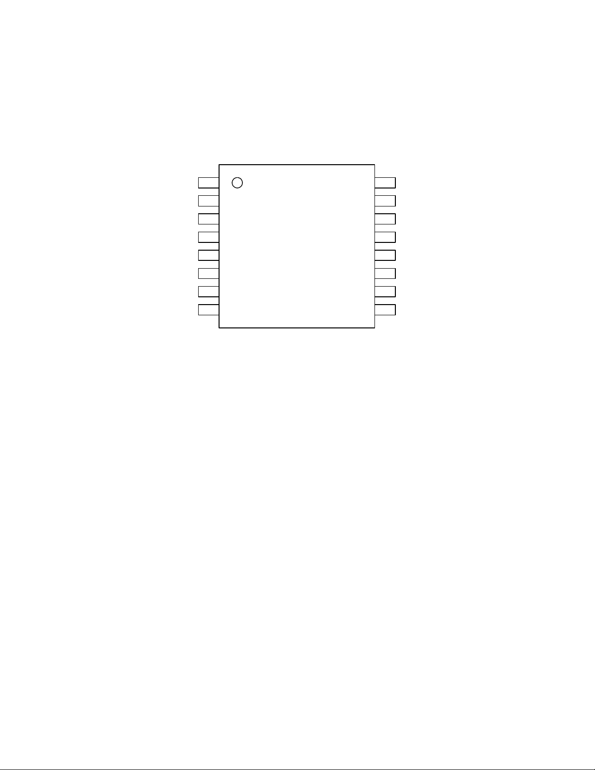
n Pin Layout
MCLK
BICK
SDTI
LRCK
PDN
DFS0
DFS1
DEM
1
2
3
4
Top View
5
6
7
8
16
15
14
13
12
11
10
9
TEST
DIF1
VDD
VSS
VCOM
LOUT
ROUT
DIF0
MS0280-E-00 2003/12
- 2 -
ASAHI KASEI [AK4386]
PIN/FUNCTION
No. Pin Name I/O Function
1 MCLK I Master Clock Input Pin
2 BICK I Audio Serial Data Clock Pin
3 SDTI I Audio Serial Data Input Pin
4 LRCK I Input Channel Clock Pin
5 PDN I
6 DFS0 I Sampling Speed Select 0 Pin
7 DFS1 I Sampling Speed Select 1 Pin
8 DEM I
9 DIF0 I Audio Interface Format 0 Pin
10 ROUT O Rch Analog Output Pin
11 LOUT O Lch Analog Output Pin
12 VCOM O
13 VSS - Ground Pin
14 VDD 15 DIF1 I Audio Interface Format 1 Pin
16 TEST I
Note: All digital input pins should not be left floating.
Full Power Down Mode Pin
“L” : Power down, “H” : Power up
De-emphasis Filter Enable Pin
“L” : OFF, “H” : ON (De-emphasis of fs=44.1kHz is enable.)
Common Voltage Output Pin, 0.55 × VDD
Normally connected to VSS with a 4.7µF (min. 1µF, max. 10µF) electrolytic
capacitor.
Power Supply Pin, 2.2 ∼ 3.6V
TEST Pin
This pin should be connected to VDD.
n Handling of Unused Pin
The unused output pins should be processed appropriately as below.
Classification Pin Name Setting
Analog LOUT, ROUT This pin should be open.
MS0280-E-00 2003/12
- 3 -
ASAHI KASEI [AK4386]
ABSOLUTE MAXIMUM RATINGS
(VSS=0V; Note 1)
Parameter Symbol min max Units
Power Supply VDD
Input Current, Any Pin Except Supplies IIN Digital Input Voltage VIND −0.3 VDD+0.3 V
Ambient Temperature (Powered applied) Ta −40 85 °C
Storage Temperature Tstg −65 150 °C
Note 1. All voltages with respect to ground.
WARNING: Operation at or beyond these limits may result in permanent damage to the device.
Normal operation is not guaranteed at these extremes.
−
0.3 4.6 V
±
10 mA
RECOMMENDED OPERATING CONDITIONS
(VSS=0V; Note 1)
Parameter Symbol min typ max Units
Power Supply VDD 2.2 3.0 3.6 V
Note 1. All voltages with respect to ground.
WARNING: AKM assumes no responsibility for the usage beyond the conditions in this datasheet.
MS0280-E-00 2003/12
- 4 -

ASAHI KASEI [AK4386]
ANALOG CHARACTERISTICS
(Ta=25°C; VDD=3.0V; VSS=0V; fs=44.1kHz, 96kHz; BICK=64fs; Signal Frequency=1kHz; 24bit Data;
Measurement frequency=20Hz ∼ 20kHz at fs=44.1kHz, 20Hz ∼ 40kHz at fs=96kHz; unless otherwise specified)
Parameter min typ max Units
Dynamic Characteristics:
Resolution 24 Bits
THD+N
DR (−60dBFS with A-weighted) 92 100 dB
S/N (A-weighted) 92 100 dB
Interchannel Isolation 80 100 dB
DC Accuracy:
Interchannel Gain Mismatch 0.2 0.5 dB
Gain Drift 100 - ppm/°C
Output Voltage (Note 2) 1.85 2.0 2.15 Vpp
Load Resistance (Note 3) 10 kΩ
Load Capacitance 25 pF
Power Supplies
Power Supply Current
Normal Operation (PDN pin = “H”, fs=44.1kHz)
Normal Operation (PDN pin = “H”, fs=96kHz)
Power Save mode (PDN pin = “H”, MCLK Stop)
Full Power-down mode (PDN pin = “L”) (Note 4)
Note 2. Full-scale voltage (0dB). Output voltage scales with the voltage of VDD, Vout = 0.67 × VDD (typ).
Note 3. For AC-load.
Note 4. All digital input pins are fixed to VDD or VSS.
fs=44.1kHz
BW=20kHz
fs=96kHz
BW=40kHz
0dBFS
−
60dBFS
0dBFS
−60dBFS
−86
−37
−84
−34
6
6.5
1.5
10
−76
-
-
-
9
10
2.5
50
dB
dB
dB
dB
mA
mA
mA
µ
A
MS0280-E-00 2003/12
- 5 -
 Loading...