

ASAHI KASEI AK4358 User Manual
ASAHI KASEI [AK4358]
192kHz 24-Bit 8ch DAC with DSD Input
A K4358
GENERAL DESCRIP TION
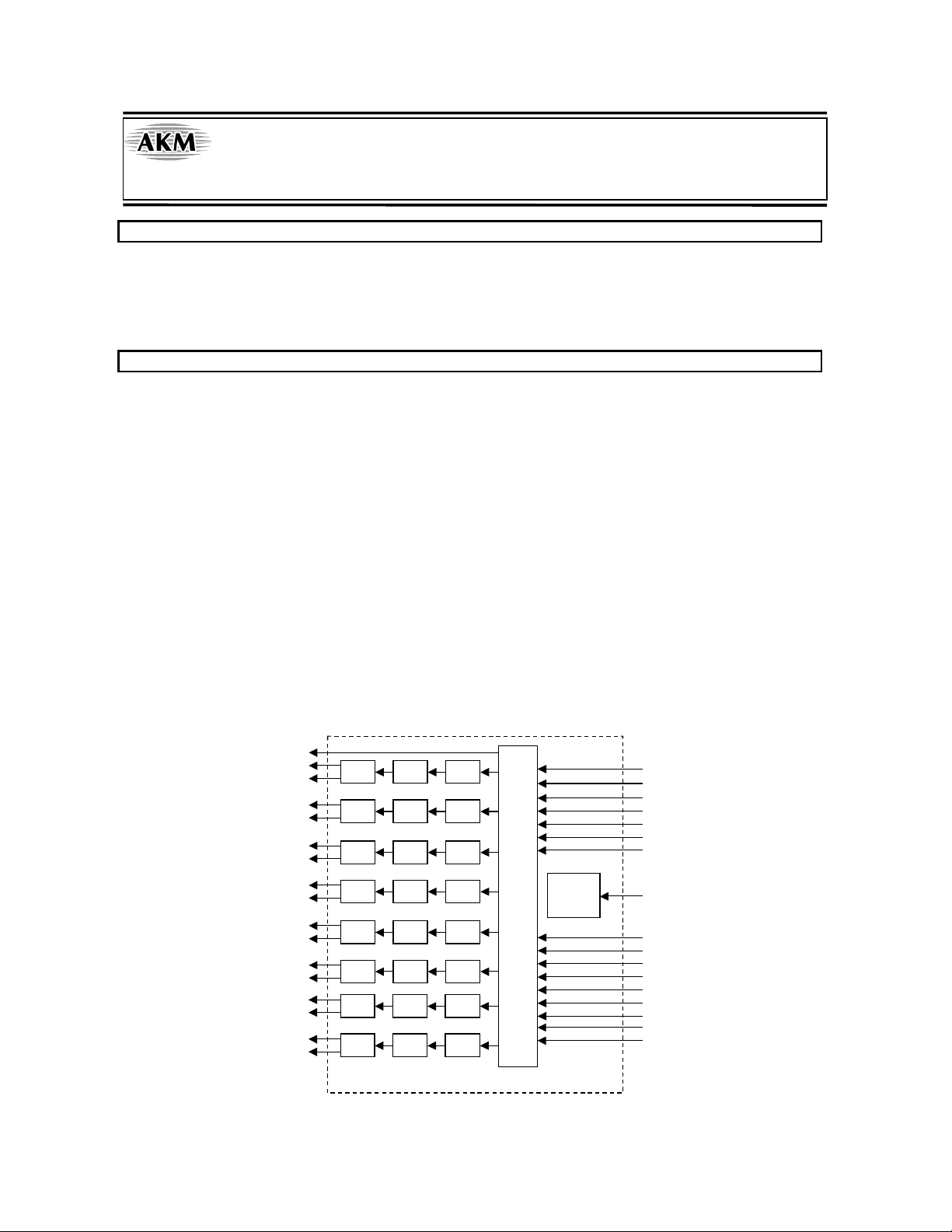
The AK4358 is eight channels 24bit DAC corresponding to digital audio syst em. Using AKM's advanced
multi bit architecture for its modulator the AK4358 delivers a wide dynamic range while preserving
linearit y f or im proved THD+N per formance. Th e A K 4358 has f ull differential S CF outputs, remov ing the
need for AC cou pling capacitors and increasing performance for systems with excessive clock jitter. The
AK4358 a cce pts 192kHz PCM data and 1-Bit DSD data, ideal for a wide range of applications including
DVD-Audio and S ACD.
FEATURES
Sampling Rate Ranging from 8kHz to 192kHz
24Bit 8 times Digital Filter with Slow roll-off option
THD+N: -94dB
DR, S/N: 112dB
High Tolerance to Clock Jitter
Low Distortion Differe n tial Output
DSD Data input available
Digital De-emphasis for 32, 44.1 & 48kHz sampling
Zero Detec t functi on
Channel Ind ep e n de nt Digi tal Attenuator with soft-tran s i tion (3 Spe ed mode)
Soft Mute
3-wire Serial and I
I/F format: MSB justified, LSB justified (16bit, 20bit, 24bit), I
2
C Bus µP I/F for mode setting
2
S, TDM or DSD
Master clock: 256fs, 384fs, 512fs or 768fs (PCM Normal Speed Mode)
128fs, 192fs , 25 6fs or 384fs (PCM Double Speed Mode)
128fs or 192fs (PCM Quad Speed Mode)
512fs or 768fs (DSD Mode)
Power Supply: 4.75 to 5.25V
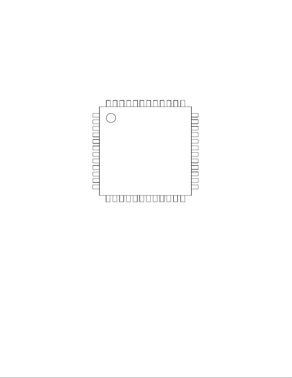
48pin LQFP Packag e
DZF
LOUT1+
LOUT1-
ROUT1+
ROUT1-
LOUT2+
LOUT2-
ROUT2+
ROUT2-
LOUT3+
LOUT3-
ROUT3+
ROUT3-
LOUT4+
LOUT4-
ROUT4+
ROUT4-
SCF
SCF DAC
SCF DAC
SCF
SCF DAC
SCF DAC
SCF DAC
SCF
DAC
DAC
DAC
DATT
DATT
DATT
DATT
DATT
DATT
DATT
DATT
Audio
I/F
PCM
DSD
Control
Register
MCLK
LRCK
BICK
SDTI1
SDTI2
SDTI3
SDTI4
3-wire
or I2C
DCLK
DSDL1
DSDR1
DSDL2
DSDR2
DSDL3
DSDR3
DSDL4
DSDR4
AK4358
MS0203-E-01 2006/02
- 1 -
ASAHI KASEI [AK4358]
K
K
Ordering Guide
AK4358VQ -40 ∼ +85°C 48LQFP
AKD4358 Evaluation Board for AK4358
Pin Layout
43
ROUT1+
ROUT1- 47LOUT2+
LOUT2-
ROUT2+
ROUT2-
LOUT3+
ROUT3+ 40ROUT3- 39LOUT4+ 38
LOUT3-
LOUT1-
LOUT1+
DZF3 3
DZF2 4
DZF1
CAD0 6
ACKSN 7
PDN 8
BIC
MCL
DVDD
DVSS 12 25 DSDL1
48
1
2
5
9
10
11
13
SDTI4
45
46
AK435 8VQ
15
14
16
SDTI1
SDTI2
SDTI3
44
Top View
17
18
I2C
LRCK
42
41
20
CDTI/SDA
CCLK/SCL 19
21
CSN/CAD1
LOUT4-
37
36
35
34
33
32
31
30
29
28
27
26
24
23
22
DCLK
DSDL4
DSDR4
AVSS
AVDD
VREFH
ROUT4+
ROUT4DIF0
DSDR3
DSDL3
DSDR2
DSDL2
DSDR1
MS0203-E-01 2006/02
- 2 -
ASAHI KASEI [AK4358]
Compatibility with AK4357
1. Function & Performance
Functions AK4357 AK4358
# of channels 6 8
DR 106dB 112dB
48kHz/96kHz TDM Not available Available
I2C Not available Available
DSDM control Pin/Register Register
Input channel of DZF pin Fixed Programm able
2. Pin Configuration
Pin # AK4357 AK4358
3 DZFL1 DZF3
4 DZFR1 DZF2
5 DZF23 DZF1
7 CAD1 ACKSN
12 NC DVSS
13 DVSS SDTI4
18 SMUTE I2C
19 CCLK CCLK/SCL
20 CDTI CDTI/SDA
21 CSN CSN/CAD1
22 DSDM DCLK
23 DCLK DSDL4
24 NC DSDR4
32 DIF1 ROUT433 DIF2 ROUT4+
37 AVSS LOUT438 AVSS LOUT4-
3. Register
Addr Bit AK4357 AK4358
00H D5 DZFM 0
01H D6 0 PW4
04H D7 ATT7 ATTE
05H D7 ATT7 ATTE
06H D7 ATT7 ATTE
07H D7 ATT7 ATTE
08H D7 ATT7 ATTE
09H D7 ATT7 ATTE
0AH D7, D6 0, 0 TDM1, TDM0
0BH Not available LOUT4 ATT Control
0CH Not available ROUT4 ATT Control
0DH Not available DZF1 control
0EH Not available DZF2 control
0FH Not available DZF3 control
MS0203-E-01 2006/02
- 3 -
ASAHI KASEI [AK4358]
PIN/FUNCTION
No. Pin Name I/O Function
1 LOUT1- O DAC1 Lch Negative Analog Output Pin
2 LOUT1+ O DAC1 Lch Positive Analog Output Pin
3 DZF3 O Zero Input Detect 3 Pin
4 DZF2 O Zero Input Detect 2 Pin
5 DZF1 O Zero Input Detect 1 Pin
6 CAD0 I Chip Address 0 Pin
7 AC KSN I Auto Setting Mode Disable Pin (Pull-down Pin)
“L”: Auto Setting Mode, “H”: Manual Setting Mode
8 PDN I Power-Down Mode Pin
When at “L”, the AK4358 is in the power-down mode and is held in reset.
The AK4358 should always be reset upon power-up.
9 BICK I Audio Serial Da ta Clock Pin
10 MCLK I Master Clock Input Pin
An external TTL clock should be input on this pin.
11 DVDD -
Digital Power Supply Pin, + 4.75∼+5.25V
12 DVSS - Digital Ground Pin
13 SDTI4 I DAC4 Audio Serial Data Input Pin
14 SDTI1 I DAC1 Audio Serial Data Input Pin
15 SDTI2 I DAC2 Audio Serial Data Input Pin
16 SDTI3 I DAC3 Audio Serial Data Input Pin
17 LRCK I L/R Clock Pin
18 I2C I Control Mode Select Pin
“L”: 3-wire Serial, “H”: I
19 CCLK/SCL I Control Data Clock Pi n
I2C = “L”: CCLK (3-wire Serial), I2C = “H”: SCL (I
20 CDTI/SDA I/O Cont r ol Dat a I n put Pi n
I2C = “L”: CDTI (3-wire Serial), I2C = “H”: SDA (I
21 CSN/CAD1 I Chip Select Pin
I2C = “L”: CSN (3-wire Serial), I2C = “H”: CAD1 (I
2
C Bus
2
C Bus)
2
C Bus)
2
C Bus)
22 DCLK I DSD Clock Pin
23 DSDL4 I DAC4 DSD Lch Data I n pu t Pi n
24 DSDR4 I DAC4 DSD Rch Data Input Pin
25 DSDL1 I DAC1 DSD Lch Data I n pu t Pi n
26 DSDR1 I DAC1 DSD Rch Data Input Pin
27 DSDL2 I DAC2DSD Lch Data Input Pin
28 DSDR2 I DAC2 DSD Rch Data Input Pin
29 DSDL3 I DAC3 DSD Lch Data I n pu t Pi n
30 DSDR3 I DAC3 DSD Rch Data Input Pin
31 DIF0 I Audio Data In terface Format 0 Pin
32 ROUT4- O DAC4 Rch Negative Analog Output Pin
33 ROUT4+ O DAC4 Rch Positive Analog Output Pin
34 VREFH I Positive Voltage Referen ce In pu t Pi n
35 AVDD -
Analog Power Supply Pin, +4.75∼+5.25V
36 AVSS - Analog Groun d Pin
37 LOUT4- O DAC4 Lch Negative Analog Output Pin
38 LOUT4+ O DAC4 Lch Positive Analog Output Pin
39 ROUT3- O DAC3 Rch Negative Analog Output Pin
40 ROUT3+ O DAC3 Rch Positive Analog Output Pin
41 LOUT3- O DAC3 Lch Negative Analog Output Pin
42 LOUT3+ O DAC3 Lch Positive Analog Output Pin
43 ROUT2- O DAC2 Rch Negative Analog Output Pin
44 ROUT2+ O DAC2 Rch Positive Analog Output Pin
MS0203-E-01 2006/02
- 4 -
ASAHI KASEI [AK4358]
45 LOUT2- O DAC2 Lch Negative Analog Output Pin
46 LOUT2+ O DAC2 Lch Positive Analog Output Pin
47 ROUT1- O DAC1 Rch Negative Analog Output Pin
48 ROUT1+ O DAC1 Rch Positive Analog Output Pin
Note: All input pins except pull-down pin should not be left floating.
ABSOLUT E MA XIMUM RATINGS
(AVSS, DVSS=0V; Note 1)
Parameter Symbol Min Max Units
Power Su p plies
Input Current (any pins except for supplies) IIN Analog Input Voltage VINA -0.3 AVDD+0.3 V
Digital Input Voltage VIND -0.3 DVDD+0.3 V
Ambient Operat ing T emperat ure Ta - 40 85
Storage Temperature Tstg -65 150
Note 1. All voltages with r espect to ground.
Note 2. AVSS and DVSS must be connected to the same anal og ground plane.
WARNING: Operation at or beyond these limits may result in permanent damage to the device.
Normal operation is not guaranteed at these extremes.
Analog
Digital
|AVSS-DVSS| (Note 2)
AVDD
DVDD
GND
∆
-0.3
-0.3
-
6.0
6.0
0.3
10
±
V
V
V
mA
C
°
C
°
RECOMMENDED OPERATING CONDITIONS
(AVSS, DVSS=0V; Note 1)
Parameter Symbol Min Typ Max Units
Power Su p plies
(Note 3)
Voltage Reference VREF AVDD-0.5 - AVDD V
Analog
Digital
AVDD
DVDD
4.75
4.75
5.0
5.0
5.25
5.25
V
V
Note 3. The power up sequence between AVDD and DVDD is not critical.
*AKM assumes no responsibility for the usage beyond the conditions in this datasheet.
MS0203-E-01 2006/02
- 5 -
ASAHI KASEI [AK4358]
ANALOG CHA RACT E RIS T ICS
(Ta=25°C; AVDD, DVDD=5V; VREFH=AVDD; fs=44.1kHz; BICK=64fs; Signal Frequency=1kHz; 24bit Input Data;
Measurement frequency=20Hz ∼ 20kHz; R
; unless otherwise specified)
≥2kΩ
L
Parameter Min Typ Max Units
Resolution 24 Bits
Dynamic Characteristics
THD+N
(Note 4)
fs=44.1kHz
BW=20kHz
fs=96kHz
BW=40kHz
fs=192kHz
BW=40kHz
0dBFS
-60dBFS
0dBFS
-60dBFS
0dBFS
-60dBFS
-94
-48
-92
-45
-92
-45
-86
-
-84
-
-
-
dB
dB
dB
dB
dB
dB
Dynamic Range (-60dBFS with A-weighted) (Note 5) 102 112 dB
S/N (A-weighted) (Note 6) 102 112 dB
Interchannel Isolation (1kHz) 90 100 dB
Interchannel Gain Mismatch 0.2 0.5 dB
DC Accuracy
Gain Drift 100 Output Voltage (Note 7)
2.35
±
±
2.5
2.65
±
Load Resistance (Note 8) 2
ppm/°C
Vpp
kΩ
Power Supplies
Power Suppl y Current (AVDD+DVDD)
Normal Operation (PDN = “H”, fs≤96kHz) (Note 9)
Normal Ope ration (PD N = “H” , fs=192kH z) (Note 10)
Power-Down Mode (PDN = “L”) (Note 11)
56
62
10
70
85
100
mA
mA
µA
Note 4. Measured by Audio Precision System Two. Refer to th e evaluation board manual.
Note 5. 100dB at 16bit data.
Note 6. S/N does not depend on input bit length.
Note 7. Full scale voltage (0dB). Output voltage sc ales with the voltage of VREFH pin. AOUT (typ. @0dB) =
(AOUT+)-(AOUT-) = ±2.5Vpp×VREFH/5.0
Note 8. For AC-l oad. 4kΩ for DC-l oa d
Note 9 AVDD=40mA(Typ), DVDD=12mA (Typ)@44.1k Hz&5V, 16mA(Typ)@96kHz&5V
Note 10 AV DD=40mA(Typ), DVDD=22mA(Typ)@192kHz&5V
Note 11. All digital inputs including clock pins (MCLK, BICK and LRCK) are held DVDD or DVSS.
MS0203-E-01 2006/02
- 6 -
ASAHI KASEI [AK4358]
SHARP ROLL-OFF FILTER CHARACTERISTICS
(Ta = 25°C; AVDD, DVDD = 4.75 ∼ 5.25V; fs = 44.1kHz; DEM = OFF; SLOW = “0”; PCM Mode)
Parameter Symbol Min Typ Max Units
Digital filter
Passband ±0.05dB (Note 12)
-6.0dB
Stopband (Note 12) SB 24.1 kHz
Passband Ripple PR
Stopband Attenuation SA 54 dB
Group Delay (Note 13) GD - 19.1 - 1/fs
Digital Filter + SCF
Frequency Response
Note 12. The passband and stopband frequencies scale with fs(system sampling rate). For example, PB=0.4535×fs
(@±0.05dB), SB=0.546×fs.
Note 13. The c alculating delay time w hich occurred by digital filtering. This time is from setting the 16/24bit data of both
channels to input register to the output of analog signa l.
20.0kHz
40.0kHz
80.0kHz
Fs=44.1kHz
Fs=96kHz
Fs=192kHz
PB 0 -
22.05
FR
FR
FR
-
-
-
±
±
+0/-0.6
0.2
0.3
20.0
0.0 2
±
kHz
-
-
-
-
kHz
dB
dB
dB
dB
SLOW ROLL-OFF FILTER CHARACTERISTICS
(Ta = 25°C; AVDD, DVDD = 4.75~5.25V; fs = 44.1kHz; DEM = OFF; SLOW = “1”; PCM Mode)
Parameter Symbol Min Typ Max Units
Digital F ilter
Passband ±0.04dB (Note 14)
-3.0dB
Stopband (Note 14) SB 39.2 kHz
Passband Ripple PR
Stopband Attenuation SA 72 dB
Group Delay (Note 13) GD - 19.1 - 1/fs
Digital Filter + SCF
Frequency Response
20.0kHz
40.0kHz
80.0kHz
fs=44.kHz
fs=96kHz
fs=192kHz
PB
FR
FR
FR
0
-
-
-
-
18.2
+0/-5
+0/-4
+0/-5
8.1
-
0.005 dB
±
-
-
-
kHz
kHz
dB
dB
dB
Note 14. The passb and a nd stopband frequ e ncie s sc a le with fs. Fo r e xample, PB = 0.18 5× f s (@±0.04dB), SB = 0.888× f s .
DC CH ARACTERISTI CS
(Ta = 25°C; AVDD, DVDD = 4.75 ∼ 5.25V)
Parameter Symbol Min Typ Max Units
High-Level Input Voltage
Low-Level Input Voltage
High-Level Output Voltage (Iout = -80µA)
Low-Level Output Voltage (Iout = 80µA)
Input Leakage Current (Note 15) Iin - -
Note 15. ACKSN pin has internal pull-down devices, nominally 100kΩ.
MS0203-E-01 2006/02
- 7 -
VIH
VIL
VOH
VOL
2.2
-
DVDD-0.4
-
-
-
- -
0.8
0.4
±
-
10
V
V
V
V
µA
ASAHI KASEI [AK4358]
SWITCHING CHARACTERISTICS
(Ta = 25°C; AVDD, DVDD = 4.75 ∼ 5.2 5V ; CL = 20pF)
Parameter Symbol Min Typ Max Units
Master Clock Frequency
Duty Cycle
LRCK Frequency
Normal Mode (TDM0= “L”, TDM1= “L”)
Norma l Speed Mode
Double Speed Mode
Quad Speed Mode
Duty Cycle
TDM256 mode (TDM0= “H”, TDM1= “L”)
Normal Speed Mode
High time
Low time
TDM128 mode (TDM0= “H”, TDM1= “H”)
Normal Speed Mode
Double Speed Mode
High time
Low time
PCM Audio Interface Timing
BICK Period
BICK Pulse Width Low
Pulse Width High
BICK “↑” to LRCK Edge (Note 16)
LRCK Edge to BICK “↑” (Note 16)
SDTI Hold Time
SDTI Setup Time
DSD Audio Interface Timing
DCLK Period
DCLK Pulse Width Low
Pulse Width High
DCLK Edge to DSDL/R (Note 17)
Control Interface Timing (3-wire Serial mode):
CCLK Period
CCLK Pulse Width Low
Pulse Width High
CDTI Setup Time
CDTI Hold Time
CSN High Time
CSN “↓” to CCLK “↑”
CCLK “↑” to CSN “↑”
Control Interface Timing (I2C Bus mode):
SCL Clock Frequency
Bus Free Time Between Transmissions
Start Condition Hold Time (prior to first clock pulse)
Clock Low Time
Clock High Time
Setup Time for Repeated Start Condition
SDA Hold Time from SCL Falling (Note 18)
SDA Setup Time from SCL Rising
Rise Time of Both SDA and SCL Lines
Fall Time of Both SDA and SCL Lines
Setup Time for Stop Condition
Pulse Widt h o f Spike Noise Su ppre ss e d b y Input Filter
fCLK
dCLK
fsn
fsd
fsq
Duty
fsn
tLRH
tLRL
fsn
fsd
tLRH
tLRL
tBCK
tBCKL
tBCKH
tBLR
tLRB
tSDH
tSDS
tDCK
tDCKL
tDCKH
tDDD
tCCK
tCCKL
tCCKH
tCDS
tCDH
tCSW
tCSS
tCSH
fSCL
tBUF
tHD:STA
tLOW
tHIGH
tSU:STA
tHD:DAT
tSU:DAT
tR
tF
tSU:STO
tSP
2.048
40
8
60
120
45
32
3/256fs
3/256fs
32
60
3/128fs
3/128fs
81
30
30
20
20
10
10
1/64fs
160
160
-20
200
80
80
40
40
150
50
50
-
4.7
4.0
4.7
4.0
4.7
0
0.25
-
-
4.0
0
11.2896 36.864
60
48
96
192
55
48
48
96
20
100
1.0
0.3
50
MHz
%
-
-
-
-
-
-
-
-
kHz
kHz
kHz
%
kHz
ns
ns
kHz
kHz
ns
ns
ns
ns
ns
ns
ns
ns
ns
ns
ns
ns
ns
ns
ns
ns
ns
ns
ns
ns
ns
kHz
µ
µ
µ
µ
µ
µ
µ
µ
µ
µ
ns
s
s
s
s
s
s
s
s
s
s
MS0203-E-01 2006/02
- 8 -

ASAHI KASEI [AK4358]
Parameter Symbol Min Typ Max Units
Reset Timing
PDN Pulse Width (Note 19)
tPD
150
ns
Note 16. BICK rising edge must not occur at the same time as LRCK edge.
Note 17. DSD data transmitting device must meet this tim e.
Note 18. Data must be held for sufficient time to bridge the 300 ns transition time of SCL.
Note 19. The AK4358 can be reset by bringing PDN= “L”.
2
Note 20. I
C is a registered trademark of Philips Semiconductors.
MS0203-E-01 2006/02
- 9 -

ASAHI KASEI [AK4358]
Timing Diagram
1/fCLK
MCLK
tCLKH
tCLKL
dCLK=tCLKH x fCLK, tCLKL x fCLK
VIH
VIL
1/fs
LRCK
VIH
VIL
tBCK
BICK
tBCKH
tBCKL
VIH
VIL
Clock Timing
LRCK
tBLR
tLRB
VIH
VIL
BICK
SDTI
tSDS
tSDH
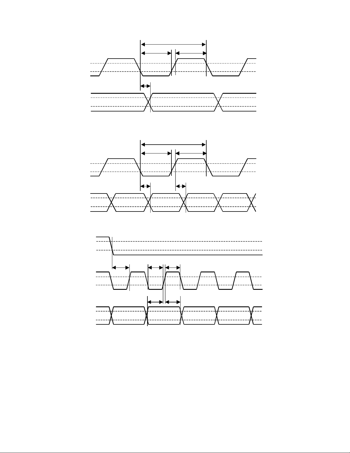
Audio Serial Interface Timing (PCM Mode)
VIH
VIL
VIH
VIL
MS0203-E-01 2006/02
- 10 -
ASAHI KASEI [AK4358]
tDCK
tDCKHtDCKL
DCLK
tDDD
DSDL
DSDR
VIH
VIL
VIH
VIL
Audio Serial Interface Timing (DSD Nor mal Mode, DCKB = “0”)
tDCK
tDCKHtDCKL
DCLK
DSDL
DSDR
tDDD
tDDD
VIH
VIL
VIH
VIL
Audio Serial Interface Timing (DSD Phase M odulation Mode, DCKB = “0”)
CSN
CCLK
CDTI
tCSS
C1 C0 R/W A4
tCCKL tCCKH
tCDS tCDH
WRITE Command Input Timing
VIH
VIL
VIH
VIL
VIH
VIL
MS0203-E-01 2006/02
- 11 -
 Loading...