

ASAHI KASEI AK4351 User Manual
K
K
e
K
查询AK4351供应商
ASAHI KASEI [AK4351]
AK4351
18Bit Advanced Multi Bit DS 2ch DAC
GENERAL DESCRIPTIO N
The AK4351 is a high cost performance 18bit stereo DAC for low-end digital audio systems. The
modulator in the AK4351 uses the new developed Advanced Multi Bit architecture with wide dynamic
range. The analog outputs are filtered in the analog domain by a combination of SCF and CTF.
Therefore, any external filters are not required. The SCF techniques also improve the loss of accuracy
from clock jitter. Therefore, the AK4351 is suitable for the system like STB including PLL circuit. The
AK4351 is available in very small 16pin TSSOP package, which reduces system space.
FEATURES
· Sampling Rate Ranging from 8kHz to 50kHz
· 128 times Oversampling
· Perfect filtering
18bit 8 times FIR Interpolator with 57dB attenuation
2nd order LPF
0.2dB at 20kHz
DEM
±
2
S
MCL
CKS
TST
Total Response:
· On chip Buffer with Single End Out put
· Digital de-emphasis for 44.1kHz sampling
· I/F format: MSB justified, 16/18bit LSB justified or I
· Master clock: 256fs or 384fs
· TTL Level Digital I nt er face
· THD+N: -88dB
· D-Range: 96dB
· High Tolerance to Clock Jitter
· Power supply: 4.5 to 5.5V
· Very Small Package: 16pin TSSOP (6.4mm x 5.0mm)
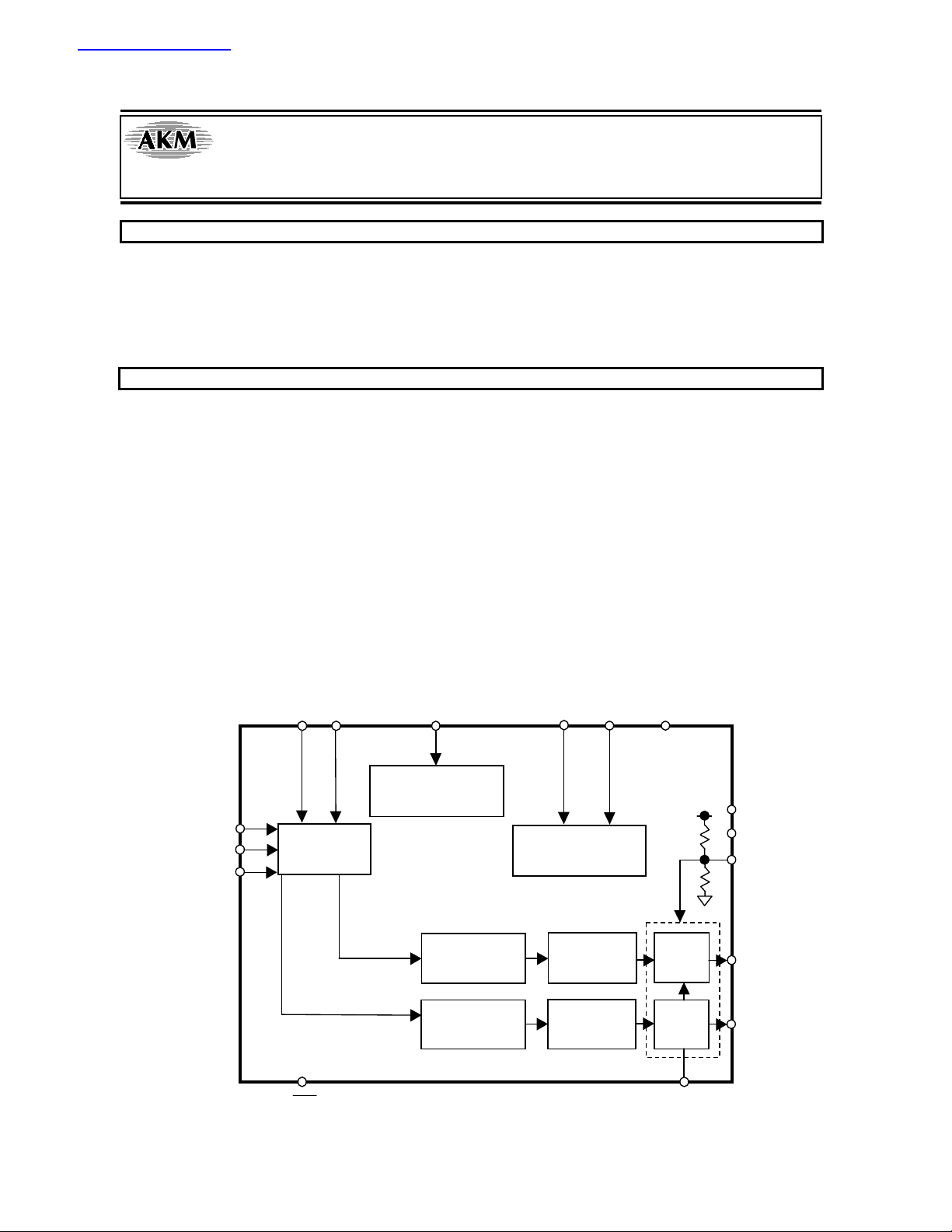
DIF0
DIF1
De-emphasis
Control
LRC
BIC
SDA TA
M0022-E-04 1999/12
Se ria l I np u t
Inte rfa c
PD
8X
Interpolator
8X
Interpolator
- 1 -
Clock Divider
DS
Modulator
DS
Modulator
LPF
LPF
VREF
VDD
VSS
VCOM
AOUTL
AOUTR
ASAHI KASEI [AK4351]
n Ordering Guide
AK4351VT -40 ~ +85°C 16pin TSSOP (0.65mm pitch)
AKD4351 Evaluation Board for AK4351
n Pin Layout
DIF0
VSS
VDD
VREF
LRCK
BICK
SDATA
1DIF1
2
3
4
Top
16
15
14
13
View
PD
MCLK
DEM
CKS
5
6
7
8
PIN/FUNCTION
No. Pin Name I/O Function
1 DIF1 I Digital Input Format Pin (Internal Pull-down pin)
2 LRCK I L/R Clock Pin
3 BICK I Audio Serial Data Clock Pin
4 SDATA I Audio Serial Data Input Pin
5
PD
6 MCLK I Master Clock Input Pin
7 DEM I De-emphasis Enable Pin
8 CKS I Master Clock Select Pin (Internal Pull-down pin)
9TST O Test Pin
10 AOUTR O Rch Analog Output Pin
11 AOUTL O Lch Analog Output Pin
12 VCOM O Common Voltage Pin, VDD/2
13 VREF I Voltage Reference Input Pin
14 VDD - Power Supply Pin
15 VSS - Ground Pin
16 DIF0 I Digital Input Format Pin (Internal Pull-down pin)
Note: All input pins except pull-down pins should not be left floating.
I Power-Down Mode Pin
When at “L”, the AK4351 is in power-down mode and is held in reset.
The AK4351 should always be reset upon power-up.
An external TTL clock should be input on this pin.
When at “H”, de-emphasis of fs=44.1kHz is enabled.
“L”: MCLK=256fs, “H”: MCLK=384fs
Must be left floating.
Normally connected to VSS with a 0.1µF ceramic capacitor in parallel with
a 10µF electrolytic cap.
The differential Voltage between this pin and VSS set the analog output range.
Normally connected to VDD.
12
11
10
VCOM
AOUTL
AOUTR
9
TST
M0022-E-04 1999/12
- 2 -
ASAHI KASEI [AK4351]
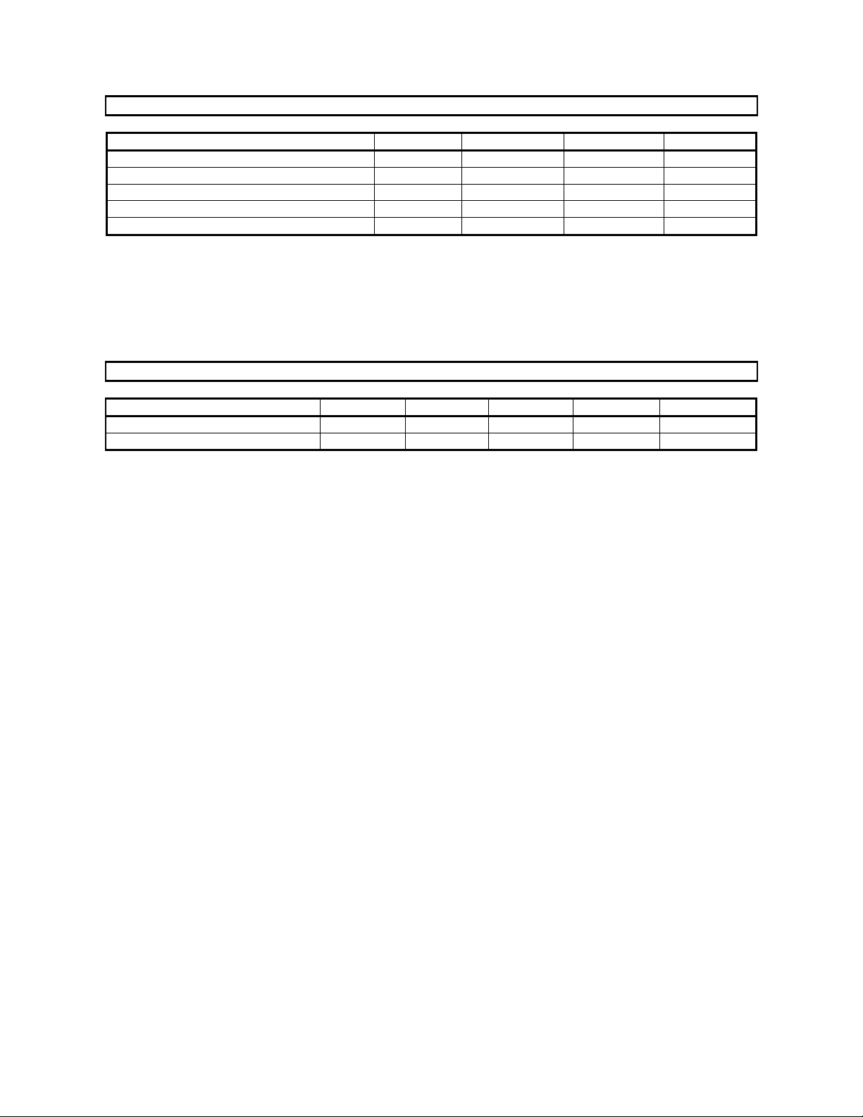
ABSOLUTE MAXI MUM RATINGS
(VSS=0V; Note 1)
Parameter Symbol min max Units
Power Supply VDD -0.3 6.0 V
Input Current, Any Pin Except Supplies IIN Input Voltage VIND -0.3 VDD+0.3 V
Ambient Operating Temperature Ta -40 85
Storage Temperature Tstg -65 150
Note:1 . All voltages with respect to ground.
WARNING: Operation at or beyond these limits may result in permanent damage to the device.
Normal operation is not guaranteed at these extremes.
10
±
mA
C
°
C
°
RECOMMENDED OPERATING CONDITIONS
(VSS=0V; Note 1)
Parameter Symbol min typ max Units
Power Supply VDD 4.5 5.0 5.5 V
Voltage Reference (Note 2) VREF 3.0 - VDD V
Note:2 . Analog output voltage scales with the voltage of VREF.
AOUT (typ.@0dB)=3.45Vpp*VREF/5.
*AKM assumes no responsibility for the usage beyond the conditions in this data sheet.
M0022-E-04 1999/12
- 3 -
ASAHI KASEI [AK4351]
ANALOG CHARACTERISTICS
(Ta=25°C; VDD=5.0V; fs=44.1kHz; BICK=64fs; Signal Frequency=1kHz; 18bit Input Data;
Measurement frequency=10Hz ~ 20kHz; R
; unless otherwise specified)
³5kW
L
Parameter min typ max Units
Resolution 18 Bits
Dynamic Characteristics (Note 3)
THD+N (0dB Output) -88 -80 dB
Dynamic Range (-60dB Output, A-weight) 90 96 dB
S/N (A-weight) 90 96 dB
Interchannel Isolation (1kHz) 96 100 dB
Interchannel Gain Mismatch 0.2 0.5 dB
DC Accuracy
Gain Drift 100 -
ppm/°C
Output Voltage (Note 4) 3.20 3.45 3.70 Vpp
Load Resistance 5
k
W
Output Current 400 µA
Power Supplies
Power Supply Current
Normal Operation ( PD
VDD
Power-Down Mode ( PD
VDD (Note 5)
=”H”)
=”L”)
14
10
20
50
mA
µA
Power Dissipation (VDD)
Normal Operation
Power-Down Mode (Note 5)
70
50
100
250
mW
µW
Power Supply Rejection (Note 6) 40 dB
Note: 3. Measured by AD725C (SHIBASOKU). Averaging mode. Refer to the evaluation board manual.
4.
Full-scale voltage (0dB). Output voltage scales with the voltage of VREF.
AOUT (typ.@0dB)=3.45Vpp*VREF/5.
5. Power Dissipation in the power-down mode is applied with no external clocks
(MCLK, BICK and LRCK held “VDD” or “VSS”).
6. PSR is applied to VDD with 1kHz, 100mVpp. VREF pin is held +5V.
M0022-E-04 1999/12
- 4 -
ASAHI KASEI [AK4351]
FILTER CHARACTERISTICS
(Ta=25°C; VDD=4.5 ~ 5.5V; fs=44.1kHz; DEM=”L”)
Parameter Symbol min typ max Units
Digital filter
Passband ±0.05dB (Note 7)
-6.0dB
Stopband (Note 7) SB 24.1 kHz
Passband Ripple PR
Stopband Attenuation SA 54 dB
Group Delay (Note 8) GD - 19.1 - 1/fs
Digital Filter + LPF
Frequency Response 0 ~ 20.0kHz
Note: 7. The passband and stopband frequencies scale with fs.
For example, PB=0.4535*fs (@±0.05dB), SB=0.546*fs.
8. The calculating delay time which occurred by digital filtering. This time is from setting the 16/18bit data of both
channels to input register to the output of analog signal.
PB 0
- 22.05
-
±
0.2
20.0
-
0.02
±
-dB
kHz
kHz
dB
DIGITAL CHARACTERISTICS
(Ta=25°C; VDD=4.5 ~ 5.5V)
Parameter Symbol min typ max Units
High-Level Input Voltage
Low-Level Input Voltage
High-Level Output Voltage (Iout=-80µA)
Low-Level Output Voltage (Iout=80µA)
Input Leakage Current (Note 9) Iin - -
VIH
VIL
VOH
VOL
2.2
-
VDD-0.4
-
-
-
--
±
0.8
0.4
10
-
V
V
V
V
µA
Note: 9. DIF0, DIF1 and CKS pins have internal pull-down devices, normally 100kW.
M0022-E-04 1999/12
- 5 -
 Loading...