

ASAHI KASEI AK4112B User Manual
ASAHI KASEI [AK4112B]
AK4112B
High Feature 96kHz 24bit DIR
GENERAL DESCRIPTION
The AK4112B is a digital audio receiver (DIR) compatible with 96kHz, 24bits. The channel status
decoding supports both consumer and professional modes. The AK4112B can automatically detect a
Non-PCM bit stream. When combined with an AK4527B multi channel codec, the two chips provide a
system solution for AC-3 applications. The dedicated pins or a serial µP I/F can control the mode setting.
The small package, 28pin VSOP or 28pin QFN saves the board space.
*AC-3 is a trademark of Dolby Laboratories.
FEATURES
o Supports AES/EBU, IEC958, S/PDIF, EIAJ CP1201
o Low jitter Analog PLL
o PLL Lock Range: 22k~108kHz
o Clock Source: PLL or X'tal
o 4 channel Receivers input and 1 through transmission output
o Auxiliary digital input
o De-emphasis for 32kHz, 44.1kHz, 48kHz and 96kHz
o Dedicated Detect Pins
- Non-PCM Bit Stream Detect Pin
- Validity Flag Detect Pin
- 96kHz Sampling Detect Pin
- Unlock & Parity Error Detect Pin
o Supports up to 24bit Audio Data Format
o Audio I/F: Master or Slave Mode
o 32bits Channel Status Buffer
o Burst Preamble bit Pc, Pd Buffer for Non-PCM bit stream
o Serial µP I/F
o Two Master Clock Outputs: 128fs/256fs/512fs
o Operating Voltage: 2.7 to 3.6V with 5V tolerance
o Small Package: 28pin VSOP, QFN
o Ta: -40~85°C
MS0078-E-00 2001/2
- 1 -
ASAHI KASEI [AK4112B]
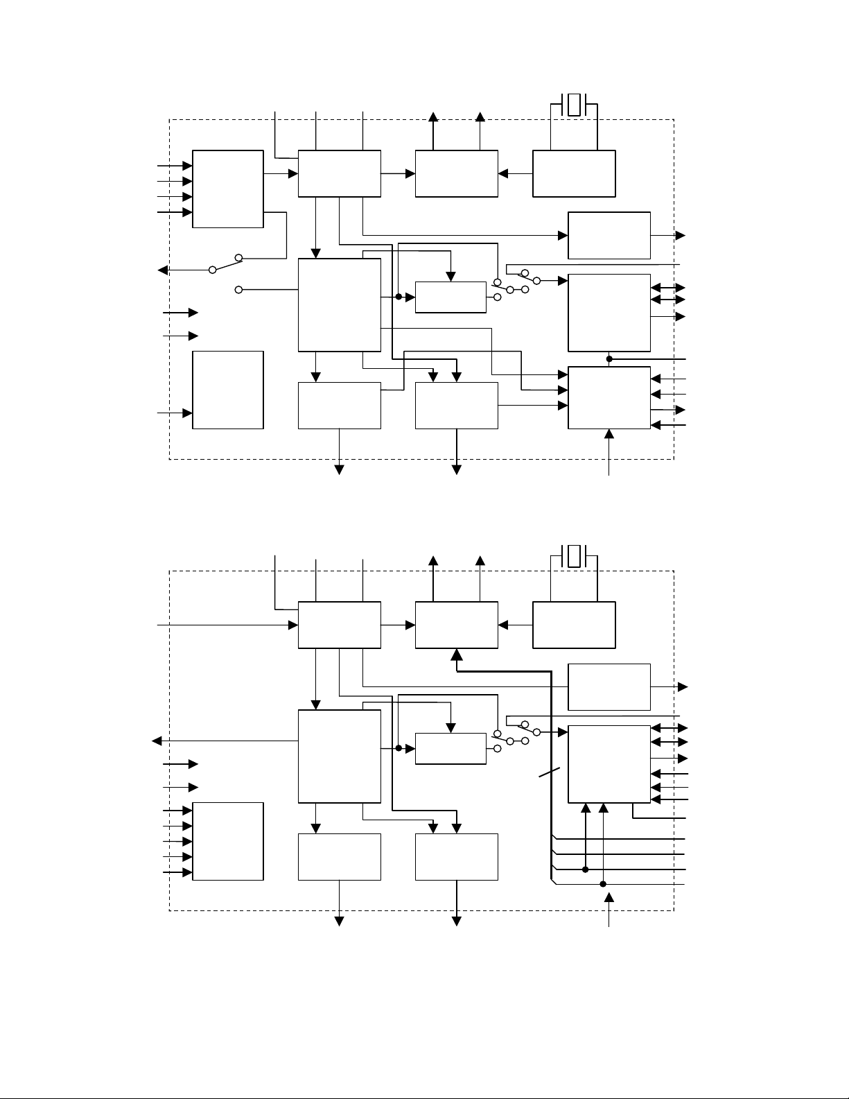
y
y
µp I/F
Audio
I/F
96kHz
Detect
y
Audio
I/F
96kHz
Detect
RX1
RX2
RX3
RX4
V/TX
DVDD
DVSS
PDN
Input
Selector
stem
S
Control
AVDDAVSS
Recover
AC-3/MPEG
Detect
R
Clock
DAIF
Decoder
AUTO ERF P/S="L"
Clock
Generator
DEM
Error
Detect
X'tal
Oscillator
XTOXTIMCKO2MCKO1
FS96
DAUX
LRCK
BICK
SDTO
TVDD
CSN
CCLK
CDTO
CDTI
RX1
V
DVDD
DVSS
OCKS0
OCKS1
CM0
CM1
PDN
System
Control
Clock
Recover
DAIF
Decoder
AC-3/MPEG
Detect
Serial Control Mode
Clock
Generator
DEM
Error
Detect
4
X'tal
Oscillator
XTOXTIMCKO2MCKO1RAVDDAVSS
FS96
DAUX
LRCK
BICK
SDTO
DIF0
DIF1
DIF2
TVDD
OCKS0
OCKS1
CM0
CM1
AUTO ERF P/S="H"
Parallel Control Mode
MS0078-E-00 2001/2
- 2 -
ASAHI KASEI [AK4112B]
n Ordering Guide
AK4112BVF -40 ~ +85 °C 28pin VSOP (0.65mm pitch)
AK4112BVN -40 ~ +85 °C 28pin QFN (0.5mm pitch)
n
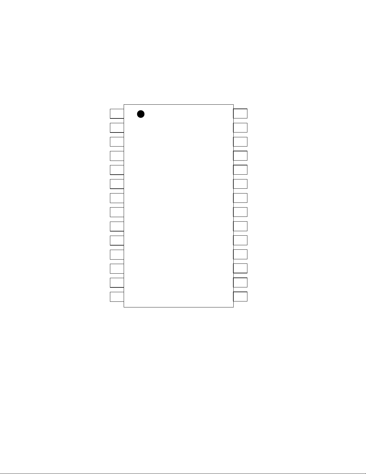
Pin Layout (AK4112BVF)
DVDD
DVSS
TVDD
V/TX
XTI
XTO
PDN 7
R
AVDD
AVSS
RX1
RX2/DIF0 12
RX3/DIF1
10
11
13
1
2
3
4
5
6
Top
View
8
9
28
27
26
25
24
23
22
21
20
19
18
17
16
CM0/CDTO
CM1/CDTI
OCKS1/CCLK
OCKS0/CSN
MCKO1
MCKO2
DAUX
BICK
SDTO
LRCK
ERF
FS96
P/SN
RX4/DIF2
14
15
AUTO
MS0078-E-00 2001/2
- 3 -
ASAHI KASEI [AK4112B]
V
X
X
A
A
2
23
22
10
13
n Pin Layout (AK4112BVN)
TVDD
DVSS
DVDD
CM0/CDTO
/TX
CM1/CDTI
7
28
26
25
24
1
OCKS0/CSN
OCKS1/CCLK
21
MCKO1
TI
TO 3
PDN 4
R
VDD 6
VSS 7
2
5
RX1 8RX2/DIF0
9
Top View
11
RX3/DIF1
RX4/DIF2
12
UTO
20
19
18
17
16
15
14
FS96
MCKO2
DAUX
BICK
SDTO
LRCK
ERF
MS0078-E-00 2001/2
- 4 -

ASAHI KASEI [AK4112B]
PIN/FUNCTION
No. Pin Name I/O Function
1 DVDD - Digital Power Supply Pin, 3.3V
2 DVSS - Digital Ground Pin
3 TVDD - Input Buffer Power Supply Pin, 3.3V or 5V
V O Validity Flag Output Pin in Parallel Mode
4
TX O Transmit channel (through data) Output Pin in Serial Mode
5 XTI I X'tal Input Pin
6 XTO O X'tal Output Pin
7 PDN I
8R 9 AVDD - Analog Power Supply Pin
10 AVSS - Analog Ground Pin
11 RX1 I
DIF0 I Audio Data Interface Format 0 Pin in Parallel Mode
12
RX2 I Receiver Channel 2 in Serial Mode
DIF1 I Audio Data Interface Format 1 Pin in Parallel Mode
13
RX3 I Receiver Channel 3 in Serial Mode
DIF2 I Audio Data Interface Format 2 Pin in Parallel Mode
14
RX4 I Receiver Channel 4 in Serial Mode
15 AUTO O
16
P/S
17 FS96 O
18 ERF O
19 LRCK I/O Output Channel Clock Pin
20 SDTO O Audio Serial Data Output Pin
21 BICK I/O Audio Serial Data Clock Pin
22 DAUX I Auxiliary Audio Data Input Pin
23 MCK02 O Master Clock #2 Output Pin
24 MCK01 O Master Clock #1 Output Pin
OCKS0 I Output Clock Select 0 Pin in Parallel Mode
25
CSN I Chip Select Pin in Serial Mode
OCKS1 I Output Clock Select 1 Pin in Parallel Mode
26
CCLK I Control Data Clock Pin in Serial Mode
CM1 I Master Clock Operation Mode Pin0 in Parallel Mode
27
CDTI I Control Data Input Pin in Serial Mode
CM0 I Master Clock Operation Mode Pin1 in Parallel Mode
28
CDTO O Control Data Output Pin in Serial Mode
Note 1: All input pins except internal pull-down pins should not be left floating.
Power-Down Mode Pin
When “L”, the AK4112B is powered-down and reset.
External Resistor Pin
18kΩ +/-1% resistor to AVSS externally.
Receiver Channel 1
This channel is selected in Parallel Mode or default of Serial Mode.
Non-PCM Detect Pin
“L”: No detect, “H” : Detect
Parallel/Serial Select Pin
I
“L”: Serial Mode, “H”: Parallel Mode
96kHz Sampling Detect Pin
(RX Mode) “H” : fs=88.2kHz or more, “L” fs=54kHz or less.
(X’tal Mode) “H” : XFS96=1, “L” : XFS96=0.
Unlock & Parity Error Output Pin
“L”: No Error, “H”: Error
MS0078-E-00 2001/2
- 5 -
ASAHI KASEI [AK4112B]
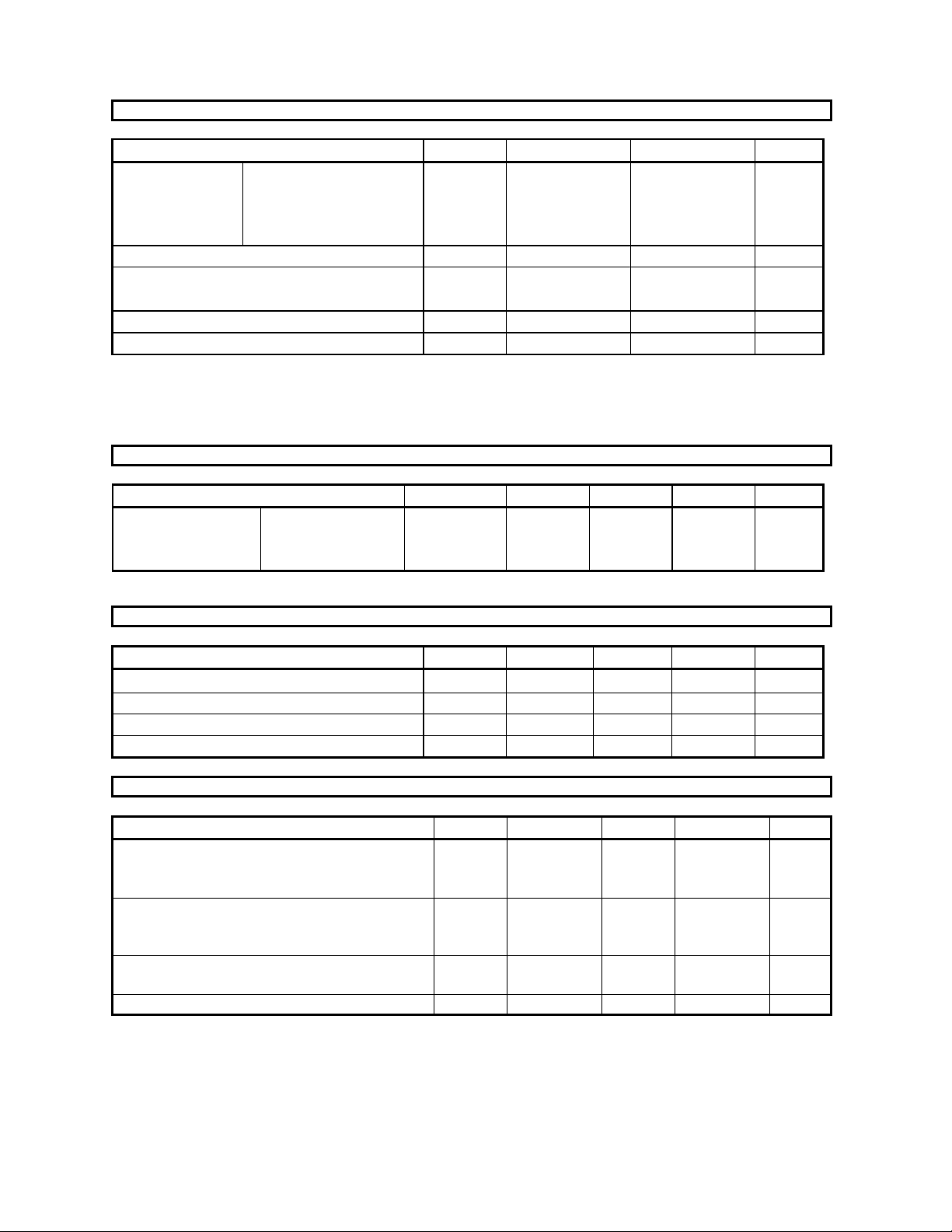
ABSOLUTE MAXIMUM RATINGS
(AVSS, DVSS=0V; Note 2)
Parameter Symbol min max Units
Power Supplies: Analog
Digital
Input Buffer
|AVSS-DVSS| (Note 3)
Input Current , Any Pin Except Supplies IIN - ±10 mA
Input Voltage (Except XTI pin)
Input Voltage (XTI pin)
Ambient Temperature (power applied) Ta -40 85 °C
Storage Temperature Tstg -65 150 °C
Note 2: All voltages with respect to ground.
Note 3: AVSS and DVSS must be connected to the same ground.
WARNING: Operation at or beyond these limits may result in permanent damage to the device.
Normal operation is not guaranteed at these extremes.
AVDD
DVDD
TVDD
∆ GND
VIN
VINX
-0.3
-0.3
-0.3
-0.3
-0.3
4.6
4.6
6.0
0.3
TVDD+0.3
DVDD+0.3
V
V
V
V
V
V
RECOMMENDED OPERATING CONDITIONS
(AVSS, DVSS=0V;Note 2)
Parameter Symbol min typ max Units
Power Supplies: Analog
Digital
Input Buffer
Note 2: All voltages with respect to ground.
AVDD
DVDD
TVDD
2.7
2.7
DVDD
3.3
3.3
3.3
3.6
AVDD
5.5
V
V
V
S/PDIF RECEIVER CHARACTERISTICS
(Ta=25°C; AVDD, DVDD=2.7~3.6V;TVDD=2.7~5.5V)
Parameter Symbol min typ max Units
Input Resistance Zin 10 kΩ
Input Voltage VTH 350 mVpp
Input Hysteresis VHY - 130 mV
Input Sample Frequency fs 22 - 108 kHz
DC CHARACTERISTICS
(Ta=25°C; AVDD, DVDD=2.7~3.6V;TVDD=2.7~5.5V; unless otherwise specified)
Parameter Symbol min typ max Units
Power Supply Current
Normal operation : PDN = “H” (Note 4)
Power down: PDN = “L” (Note 5)
High-Level Input Voltage (Except XTI pin)
High-Level Input Voltage (XTI pin)
Low-Level Input Voltage
High-Level Output Voltage (Iout=-400µA)
Low-Level Output Voltage (Iout=400µA)
Input Leakage Current Iin - - ± 10 µA
Note 4: AVDD, DVDD=3.3V, TVDD=5.0V, CL=20pF, fs=96kHz, X'tal=12.288MHz,
Clock Operation Mode 2, OCKS1=1, OCKS0=0.
AVDD=8mA(typ), DVDD=12mA(typ), TVDD=10µA(typ)
Note 5: RX inputs are open and all digital input pins are held DVDD or DVSS.
VIH
VIH
VIL
VOH
VOL
70%DVDD
70%DVDD
DVSS-0.3
DVDD-0.4
-
20
10
40
100
-
-
-
-
-
TVDD
DVDD
30%DVDD
-
0.4
mA
µA
V
V
V
V
V
MS0078-E-00 2001/2
- 6 -
ASAHI KASEI [AK4112B]
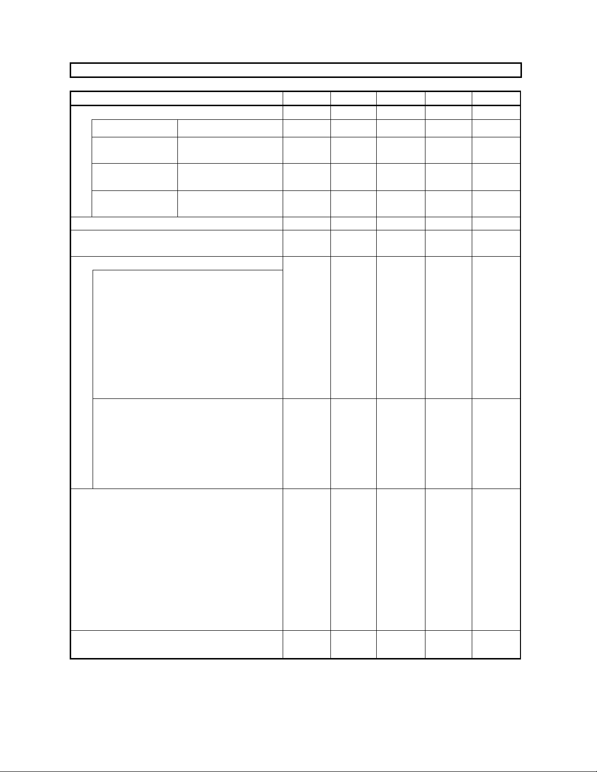
SWITCHING CHARACTERISTICS
(Ta=25°C; DVDD, AVDD2.7~3.6V, TVDD=2.7~5.5V; CL=20pF)
Parameter Symbol min typ max Units
Master Clock Timing
Crystal Resonator Frequency fXTAL 11.2896 24.576 MHz
External Clock Frequency
Duty
MCKO1 Output
MCKO2 output
PLL Clock Recover Frequency (RX1-4) fpll 22 - 108 kHz
LRCK Frequency
Duty Cycle
Audio Interface Timing
Slave Mode
BICK Period
BICK Pulse Width Low
Pulse Width High
LRCK Edge to BICK “↑” (Note 6)
BICK “↑” to LRCK Edge (Note 6)
LRCK to SDTO (MSB)
BICK “↓” to SDTO
DAUX Hold Time
DAUX Setup Time
Master Mode
BICK Frequency
BICK Duty
BICK “↓” to LRCK
BICK “↓” to SDTO
DAUX Hold Time
DAUX Setup Time
Control Interface Timing
CCLK Period
CCLK Pulse Width Low
Pulse Width High
CDTI Setup Time
CDTI Hold Time
CSN “H” Time
CSN “↓” to CCLK “↑”
CCLK "↑" to CSN “↑”
CDTO Delay
CSN “↑” to CDTO Hi-Z
Reset Timing
PDN Pulse Width tPW 150 ns
Note 6: BICK rising edge must not occur at the same time as LRCK edge.
Frequency
Duty
Frequency
Duty
fECLK
dECLK
fMCK1
dMCK1
fMCK2
dMCK2
fs
dLCK
tBCK
tBCKL
tBCKH
tLRB
tBLR
tLRM
tBSD
tDXH
tDXS
fBCK
dBCK
tMBLR
tBSD
tDXH
tDXS
tCCK
tCCKL
tCCKH
tCDS
tCDH
tCSW
tCSS
tCSH
tDCD
tCCZ
11.2896
40 50
5.632
40 50
2.816
40 50
22
45
140
60
60
30
30
20
20
-20
20
20
200
80
80
50
50
150
50
50
24.576
27.648
27.648
48 108
64fs
50
60
60
60
55
35
35
20
40
45
70
MHz
%
MHz
%
MHz
%
kHz
%
ns
ns
ns
ns
ns
ns
ns
ns
ns
Hz
%
ns
ns
ns
ns
ns
ns
ns
ns
ns
ns
ns
ns
ns
ns
MS0078-E-00 2001/2
- 7 -
ASAHI KASEI [AK4112B]
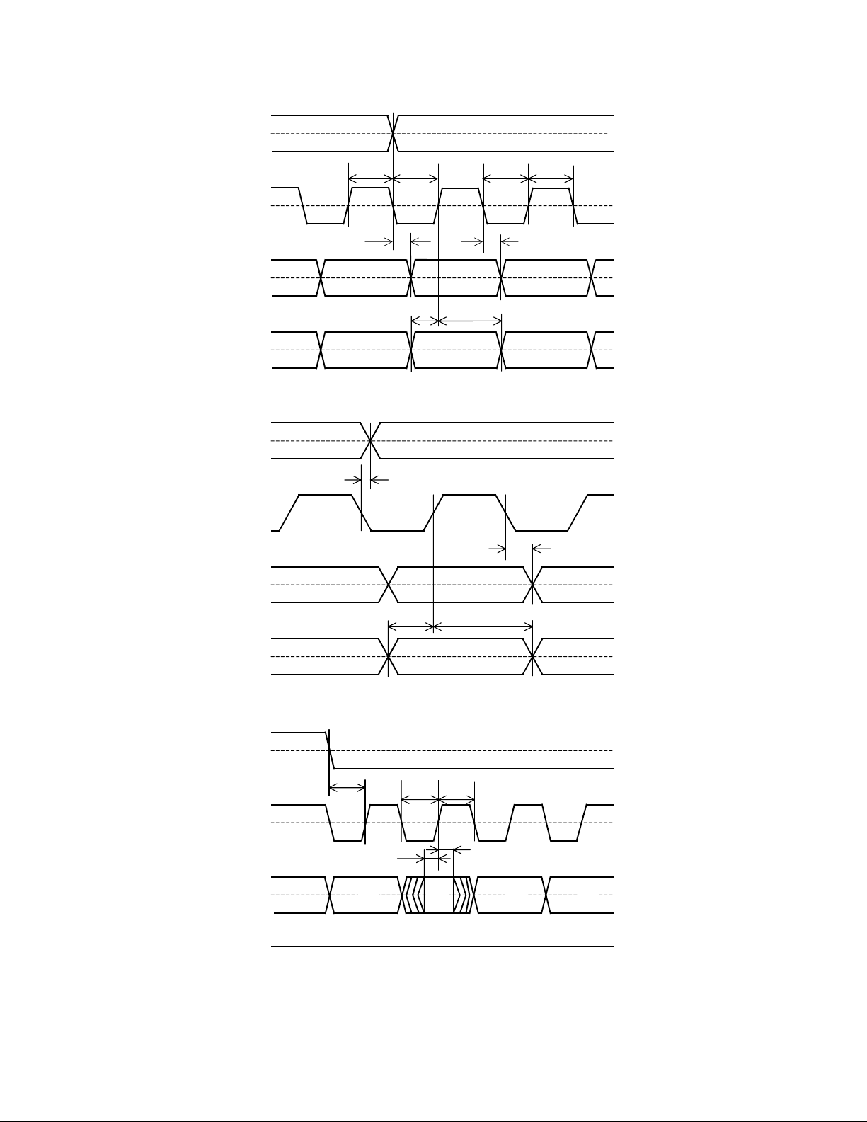
n Timing Diagram
LRCK
BICK
SDTO
DAUX
LRCK
BICK
tLRB
tBLR tBCKL tBCKH
tLRM
tDXS tDXH
Serial Interface Timing (Slave Mode)
tMBLR
50%DVDD
50%DVDD
tBSD
50%DVDD
50%DVDD
50%DVDD
50%DVDD
SDATA
DAUX
CSN
CCLK
CDTI
CDTO
tDXS
tDXH
Serial Interface Timing (Master Mode)
tCSS
C0
tCDS
tCCKL
tCCKH
tCDH
C0 A4
Hi-Z
R/W
tBSD
50%DVDD
50%DVDD
50%DVDD
50%DVDD
50%DVDD
WRITE/READ Command Input Timing
MS0078-E-00 2001/2
- 8 -
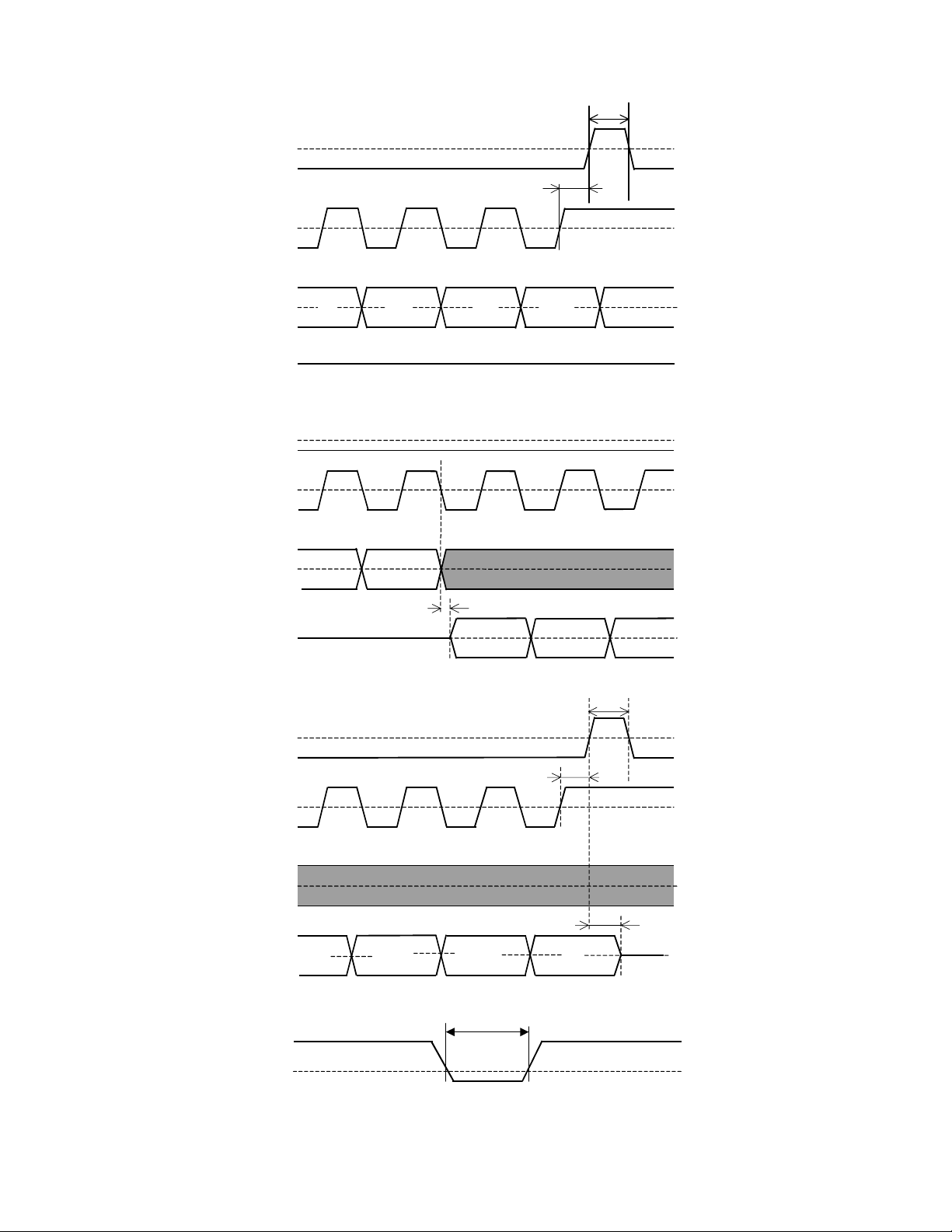
ASAHI KASEI [AK4112B]
tCSW
CSN
tCSH
CCLK
CDTI D2 D0
CDTO
D1D3
Hi-Z
WRITE Data Input Timing
CSN
CCLK
CDTI
A1 A0
50%DVDD
50%DVDD
50%DVDD
50%DVDD
50%DVDD
50%DVDD
CDTO
CSN
CCLK
CDTI
CDTO
PDN
D3
Hi-Z
READ Data Output Timing 1
D2 D1
READ Data Input Timing 2
tDCD
D7 D6
tPW
D0
tCSW
tCSH
D5
tCCZ
50%DVDD
50%DVDD
50%DVDD
50%DVDD
50%DVDD
30%DVDD
Power Down & Reset Timing
MS0078-E-00 2001/2
- 9 -

ASAHI KASEI [AK4112B]
OPERATION OVERVIEW
n Non-PCM (AC-3, MPEG, etc.) Stream Detect
The AK4112B has a Non-PCM steam auto detect function. When the 32bit mode Non-PCM preamble based on Dolby
“AC-3 Data Stream in IEC958 Interface” is detected, the AUTO goes “H”. The 96bit sync code consists of 0x0000,
0x0000, 0x0000, 0x0000, 0xF872 and 0x4E1F. Detection of this pattern will set the AUTO “H”. Once the AUTO is set
“H”, it will remain “H” until 4096 frames pass through the chip without additional sync pattern being detected. When
those preambles are detected, the burst preambles Pc and Pd that follow those sync codes are stored to registers 0DH10H.
n Clock Recovery and 96kHz Detect
On chip low jitter PLL has a wide lock range with 22kHz to 108kHz and the lock time is less than 20ms. The 96kHz
detect output pin FS96 goes “H” when the sampling rate is 88.2kHz or more and “L” at 54kHz or less. In X’tal Mode, the
FS96 pin outputs the value which is set by XFS96. PLL loses lock when the received sync interval is incorrect.
n Master Clock
The AK4112B has two clock outputs, MCKO1 and MCKO2. These clocks are derived from either the recovered clock or
from the X'tal oscillator. The frequencies of the master clock outputs (MCKO1 & MCKO2) are set by OCKS0 and
OCKS1 as shown in Table 1. 96kHz sampling is not supported at No.2.
No. OCKS1 OCKS0 MCKO1 MCKO2 X’tal fs (kHz)
0 0 0 256fs 256fs 256fs 32, 44.1, 48, 96 Default
1 0 1 256fs 128fs 256fs 32, 44.1, 48, 96
2 1 0 512fs 256fs 512fs 32, 44.1, 48
3 1 1 Test Mode
Table 1. Master clock frequencies select
n Clock Operation Mode
The CM0 and CM1 select the clock source of MCKO1/2 and the data source of SDTO via the dedicated pins or the
control register. In Mode 2, the clock source is switched from PLL to X'tal when PLL goes unlock state. In Mode3, the
clock source is fixed to X'tal, but PLL is also operating and the recovered data such as C bits can be monitored.
Mode CM1 CM0
0 0 0 - ON OFF PLL RFS96 RX
101
210
3 1 1 - ON ON X'tal XFS96 DAUX
UNLOCK
0 ON ON PLL RFS96 RX
1
ON: Oscillation (Power-up), OFF: STOP (Power-down)
PLL X'tal Clock source
OFF ON X'tal
ON ON X'tal
Table 2. Clock Operation Mode select
FS96
XFS96
XFS96
SDTO
Default
DAUX
DAUX
MS0078-E-00 2001/2
- 10 -
ASAHI KASEI [AK4112B]
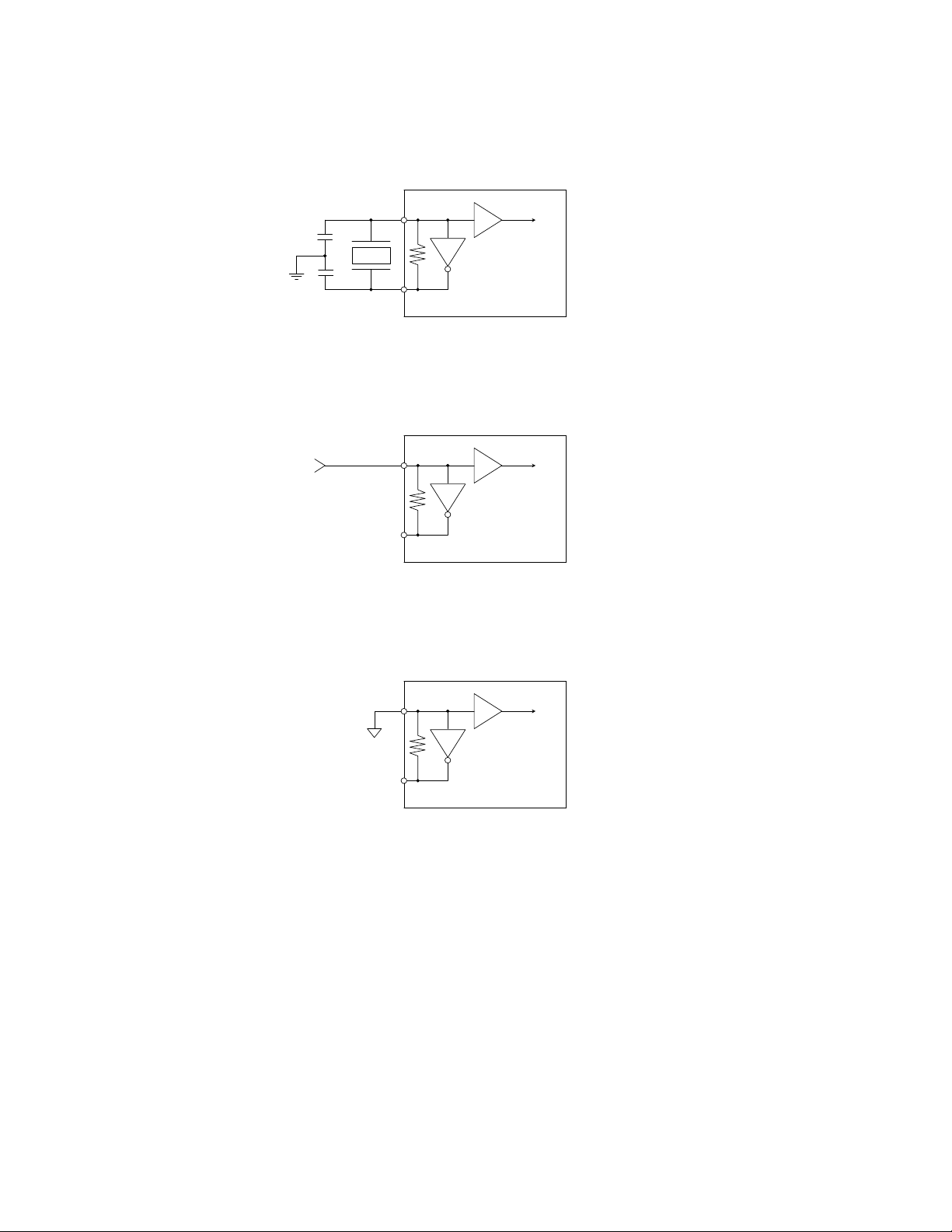
n Clock Source
The following circuits are available to feed the clock to XTI pin (#5 pin) of AK4112B.
1) X’tal
XTI
Note: External capacitance depends on the crystal oscillator (Typ. 10-40pF)
2) External clock
External Clock
3) Fixed to the Clock Operation Mode 0
XTO
AK4112B
XTI
AK4112B
XTO
Note: Input clock must not exceed DVDD.
XTI
XTO
AK4112B
MS0078-E-00 2001/2
- 11 -
 Loading...