

ASAHI KASEI AK2307, AK2307LV User Manual
ASAHI KASEI [AK2307/LV]
AK2307/LV
SPEECH CODEC for Digital Key telephone (5.0V/3.3V)
GENERAL DISCREPTION
AK2307/LV is an integrated LSI with PCM CODEC,
Voice path control, MIC amplifier and Handset driver
suitable for PBX/KTS digital key telephone, VoIP
Telephone.
PCM CODEC is compliant to ITU specification, very
low noise, and low power dissipation CODEC. A-law
and u-law selectable through Serial I/F register.
PCM I/F provides Long/Short frame format and GCI.
The output is 8bit compressed data along with 16bit
linear format.
Voice path block consists of Tone generator, Volume
for both TX and RX, Analog inputs, outputs for
Handset speaker and the speaker for hands-free
conversation, and the path control switch.
Side tone can be added internally and its volume
is controlled through serial I/F.
FEATURES
- 2 MIC AMP for the handset and microphone are
integrated.
- A 150 ohm handset driver and an extra 150 ohm
driver for a headset receiver are provided.
- Path control and volume control via serial CPU
I/F
- programmable tone generator
- 5.0V+/-5%, 3.3V+/-0.3V single power supply
- Low noise, low power consumption
Package
28pin VSOP package
- Package size; 9.8*7.6mm(pin to pin)
- Pin pitch; 0.65mm
MS0190-E-05 2005/12
1
ASAHI KASEI [AK2307/LV]
16bit Linear
BLOCK DIAGRAM
Handset Mic
I/F
HANDT4
HANDT1
HANDT2
HANDT3
External Mic
I/F
MIC3
MIC1
MIC2
DAOUT
RAIN
Handset Receiver
output
HANDR
Headset Receiver
output
HEADO
Speaker output
SPO
upto +25dB
Amp1
Amp2
150ohm Driver
Amp5
150ohm Driver
Amp10
10K ohm Driver
0dB/+3dB
0dB/+3dB
0dB/+3dB
+14dB
+14dB
24 steps
by 1dB
0 to -23dB
SW4
SW5
SW6
SW7
SW2
SW3
+0dB
VOL2
SW8
SW9
SW1
VOL3
24 steps
by 1dB
0 to -23dB
- 1
- 1
Amp3
SW10
VOL5
16 steps
by 2dB
0 to -30dB
VOL1
16 steps
by 1dB
+7 to -8dB
AGC
A/D
D/A
(Back ground
Noise ATT)
16 Steps
by 3dB
-12 to -57dB
VOL4
16 steps
by 3dB
0 to -45dB
EXRIN
Side Tone
Digital ATT
PCM CODEC
PAD
+
0/-9dB
+
0 to -21dB
+6 to -21dB
L_ATT
-2.5dB
TX Digital
Attenuator
8 steps
by 3dB
RX Digital
Volume
8 steps
by 3dB
Tone Gen H
(DTMF-H)
Tone Gen L
(DMTF-L)
Linear
A/u
Linear
A/u
Voltage Reference
DVSS
PCM
Interface
PLL
Clock generator
CPU Interface
DVDD
AVSS
AVDD
or
A/u-law
DX
DR
FS
BCLK
PLLCAP
CSN
SCLK
DATA
VREF
TAGND
RAGND
MS0190-E-05 2005/12
2

ASAHI KASEI [AK2307/LV]
VSS VDD
VREF
PIN ASSIGNMENT
HANDR
HEADO
FS
DX
BCLK
DR
DATA
SCLK
CSN
AVDD
MIC2
MIC1
1
2
TOP VIEW
3
4
5
6
7
8
9
10
11
12
13
14
28
27
26
25
24
23
22
21
20
19
18
17
16
15
PLLCAP
SPO
EXRIN
RAIN
DAOUT
RAGND
AVSS
TAGND
HANDT3
HANDT2
HANDT1
HANDT4
MIC3
MS0190-E-05 2005/12
3

ASAHI KASEI [AK2307/LV]
state output
PIN CONDITIONS
Pin types;
NIN: Normal Input
NOUT: Normal Output
TOUT: Tri-state output
AOUT: Analog output
PWR: Power supply
AIN: Analog Input
Table 1
Name Type
HANDT2 AIN Analog input for Handset microphone
HANDT3 AIN Analog input for Handset microphone
HANDT1 AOUT OPamp output for Handset microphone
HANDT4 AIN Analog input for A/D converter
HANDR AOUT Analog output for Handset receiver 1000pF 150ohm
MIC3 AIN 2nd Analog input for A/D converter
MIC2 AIN Analog input for External microphone
MIC1 AOUT Output of External microphone amplifier
DAOUT AOUT Analog output of D/A converter
RAIN AIN Analog input to RX voice path
HEADO AOUT RX output for Headset receiver 1000pF 150ohm
SPO AOUT RX output for External Speaker Driver 20pF 10kohm
EXRIN AIN External input for Speaker pre-driver
DATA I/O Data input for internal register access 50pF
SCLK NIN
CSN NIN Chip select input
DR NIN RX PCM data serial input
DX TOUT TX PCM data serial output. TriBCLK NIN Bit clock input for DR, DX
FS NIN 8KHz frame sync signal input for PCM I/F
DVSS PWR Power supply for digital block:0V
DVDD PWR Power supply for digital block: 3.3V
AVSS PWR Power supply for Analog block:0V
AVDD PWR Power supply for Analog block: 3.3V
PLLCAP AOUT
TAGND AOUT TX side Analog ground output.
RAGND AOUT RX side Analog ground output
VREF AOUT Voltage reference output
Serial data clock for internal register
access
Output to connect the PLL loop filter
Capacitance
Pin function
Max
Cap load
50pF
MIn
Res load
comment
1.0uF external
capacitance
1.0uF external
capacitance
1.0uF external
capacitance
1.0uF external
capacitance
MS0190-E-05 2005/12
4
ASAHI KASEI [AK2307/LV]
ABSOLUTE MAXIMUM RATINGS
Parameter Symbol Min Max Units
Power Supply Voltages
Analog/Digital Power Supply
VSS Voltage VSS -0.1 0.1 V
Digital Input Voltage VTD -0.3 VDD+0.3 V
Analog Input Voltage VTA -0.3 VDD+0.3 V
Input current (except power supply pins) IIN -10 10 mA
Storage Temperature Tstg -55 125 oC
Warning: Exceeding absolute maximum ratings may cause permanent damage.
Normal operation is not guaranteed at these extremes.
VDD
-0.3
6.5
V
RECOMMENDED OPERATING CONDITIONS
Parameter Symbol Min Typ Max Units
Power Supplies
Analog/Digital power supply( AK2307LV)
Analog/Digital power supply( AK2307) VDD 4.75 5.0 5.25 V
Ambient Operating Temperature Ta -10 85
Frame Sync Frequency FS - 8 - kHz
Note) All voltages reference to ground : VSS=0V
VDD
3.0
3.3
3.6
V
o
C
MS0190-E-05 2005/12
5
ASAHI KASEI [AK2307/LV]
FUNCTIONAL DISCRIPTIONS
1. SERIAL INTERFACE
The internal registers can be read/written via serial CPU interface which consists of SCLK, DATA, and CSN
pin.
1 word consists of 16bits. The first 3bits are the instruction code which specifies read or write.
The following 4bits specify the address. The rest of 8bits are the data stored in the internal registers.
Table1-A CPU I/F ADDRESS/DATA STRUCTURE
B15 B14 B13 B12 B11 B10 B9 B8 B7 B6 B5 B4 B3 B2 B1 B0
I2 I1 I0 A3 A2 A1 A0 * D7 D6 D5 D4 D3 D2 D1 D0
Instruction code
(3 bit )
*)Dummy bit for adjusting the I/O timing when reading register.
Table1-B INSTRUCTION CODE
I2 I1 I0
1 1 0
1 1 1
Others
Address
(4bit)
*
Data for internal registers
(8bit)
Read/Write
Read
Write
No action
1-2 Timing of the Serial Interface
SCLK and DATA timing in WRITE/READ operation
(1) Input data are loaded into the internal shift register at the rising edge of SCLK.
(2) The rising edge of SCLK is counted after the falling edge of CSN.
(3) When CSN is “L” and more than 16 SCLK pulses:
[WRITE] Data are loaded into the internal register at the rising edge of the SCLK 16th pulse.
[READ] DATA pin becomes an input pin at the falling edge of the SCLK 16th pulse.
CSN timing and WRITE/READ CANCELLATION
(1) WRITE is cancelled when CSN goes up before the rising edge of the SCLK 16th pulse.
(2) READ is cancelled when CSN goes up before the falling edge of the SCLK 16th pulse.
SERIAL WRITE/READ ACCESS timing (SERIAL ACCESS MODE)
(1) Serial write and read operation will be done by feeding the another 16 SCLK pulse and
data after 1st write or read operation.
(2) It is not necessary to make CSN high between 1st operation and 2nd operation.
MS0190-E-05 2005/12
6

ASAHI KASEI [AK2307/LV]
ZZZ
Write data
Z
Z
Z
WRITE
Continuous SCLK
Goes up anytime
CSN
after SCLK 16th pulse and before 32nd pulse
SCLK
DATA
2 3 41
1 1
Instruction
Code
1 0
6 7 85 15 16
0 0 0 *
Address
“0000”
9 16
D7
Write data to
address”000”
D0
WRITE at the rising
edge of SCLK 16
pulse
th
2 3 41
1 1
Instruction
Code
8 9
1
D7
D1
Burst SCLK
SCLK can be stoped at “H” level or “L” level at anytime during the write cycle. After resuming the SCLK, write cycle is
retrieved normally.
Goes up anytime
CSN
SCLK
DATA
2 3 41
Z
1 1
Instruction
Code
1 0
6 7 85
0 0 0 *
Address
”0000”
9 16
D7
Write data to
address “000”
D0
WRITE at the rising
edge of SCLK 16
pulse
after SCLK 16th pulse and 32nd pulse
th
CANCELLATION
CSN goes “H” before the rising
CSN
edge of 16th SCLK pulse
D0
SCLK
DATA
Z
2 3 41
1 1
Instruction
Code
1 0
6 7 85
0 0 0 *
Address
”0000”
9 16
D7
Write data to
address”000”
D0
Write is not
Excuted
DATA pin: Input mode
(Hi-Z)
MS0190-E-05 2005/12
7

ASAHI KASEI [AK2307/LV]
Address
Address
Write data
ZZZ
EXCUTED!
EXCUTE!
Address
A2
A1D7ZZZ
A3
Data output starts at the falling edge of SCLK 8
th
pulse
Read Data
Z
A3
Read output starts at the falling edge of SCLK 8
th
pulseD7Address
A2
A1
SERIAL ACCESS
Serial access can be done by CSN staying “L” during the serise of write cycle.
CSN
SCLK
DATA
1 1
Instruction
Code
READ
Continuous SCLK
CSN
SCLK
DATA
1 1
Instruction
2 3 41
1 0
2 3 41
0
6 7 85 15 16
0 0 0 *
”0000”
6 7 85 15 16
A0 Z
9 16
D7
Write data to
”000”
9 16
Read DataRead
D0
D0
2 3 41
1 1
Can be going up at anytime
after SCLK 16th pulse and before 32nd pulse
Read period
until the earlier edge of either CSN rising or SCLK 16th pulse
falling
Instruction
Code
2 3 41
1 1
Instruction
1 1
1 0
8 9
D7
8 9
D7
D1
D0
D1
Read DataRead
D0
Burst SCLK
CSN
SCLK
DATA
Z
1 1
Read
Instruction
Can be going up at anytime
after SCLK 16th pulse and before 32nd pulse
2 3 41
0
6 7 85
A0 Z
9 16
D0
MS0190-E-05 2005/12
8
ASAHI KASEI [AK2307/LV]
Read data
Z
Z
A2
A1
SERIAL ACCESS
Serial access can be done by CSN staying “L” during the serise of read cycle
CSN
SCLK
DATA
2 3 41
Z Z
1 1
Read
Instruction
0
0
6 7 85 15 16
0 0 0
Address
”0000”
9 16
D7
D0
READ
EXCUTED!
1 1
2 3 41
1 0
Read
Instruction
8 9
READ
EXCUTED!
DISCORD OF INSTRUCTION CODE
CSN
SCLK
DATA
2 3 41
I2 I1
IInstructions except specified
0bb
10b
(b=0 or 1)
I0 IA3
6 7 85
A0
Address
9 16
WRITE/READ
NOT EXCUTED!
ZZ
DATA pin: Input mode
Z
(Hi-Z)
Register Map
Register Type : Read/ Write
Add
(Hex)
B – F
Address “1” ; PCM_1/2 ---- Selection of the PCM interface Mode(Long/Short frame, AK130-1,AK130-2, 16bit linear)
Address ”6” ; L-ATT ---- -6dB attenuation for Tone generator-L output in case of DTMF tone generation.
D7 D6 D5 D4 D3 D2 D1 D0 Register Name
(Functions)
0 SW8
1 RX_
A_gain
SW7 SW6
RX Pad
-9dB
Side
Tone
SW5 SW4 SW3 SW2 SW1
PCM_1 PCM_0 u/A-law SW10 SW9
Path Control 1
Path Control 2 &
PCM Control
2 0 TX Attenuator VOL1 TX Digital Volume Control
3
RX Volume Side Tone Attenuator RX Digital Volume Control
4 0 0 0 0 VOL4 Tone Volume Control
5 0 0 Tone Freq. Select Tone Generator 1
6 0 L-ATT Tone Freq. Select Tone Generator 2
7 0 0 0 VOL2 RX Handset Volume Control
8 0 0 0 VOL3 RX Headset Volume Control
9
- - - - VOL5 RX Speaker Volume Control
A
- AGC_ON
Falling time Rising time Threshold level
AGC Control
- - - - - - - - Reserved for test use
Bits in which “0” is filled are for test mode activation. Please fill the data “0” for the normal operation.
Bits in which “-“ is filled are for test use and can not write the data from CPU interface. In case the read
operation, data “0” are read from CPU interface.
MS0190-E-05 2005/12
9
ASAHI KASEI [AK2307/LV]
2. PCM Data Interface
AK2307/LV supports 4 PCM data interface modes.
- A/u-Law PCM data mode( Long or Short frame)
This mode is for interface of 64kbps PCM data which are compressed /extended by A -law or u-law. Both Long
frame
and short frame format data are acceptable. The PCM data occupies the first time slot of the PCM data bus which
is specified by the frame sync signal. Please refer to the format diagram.
- 16 bit Linear data Mode
This mode interfaces the 16 bit linear PCM data. PCM CODEC of AK2307/LV operates at 14 bit accuracy. The 2
bits
of the LSB are fixed in the 16 bit data stream.
- AK130 B1 Mode
This mode provides the PCM data Interface to AK130, the TCM transceiver for PBX/KTS system. PCM data format
is 64kbps A-law or u-law data. The timing between data and FS is different from the A/u -Law PCM data mode
written above. In this mode the PCM data are transmitted/received via B1 channel , one of the PCM data
channel of the AK130.
- AK130 B2 Mode
This mode provides the PCM data interface to AK130 B2 channel in as same manner as AK130 B1 Mode.
In every modes, the digital voice data are in and out from DR and DX pin and the bit clock and the 8KHz frame sync
signal will be fed via BCLK and FS, respectively. The order of PCM and linear data is MSB first .
Table 2-A Summary of PCM interface modes
Mode
A/u-Law PCM data
mode
16bit Linear data
mode
AK130 B1
mode
AK130 B2
mode
2-1. Selection of the interface mode
These four interface modes are selectable through the CPU register which specified below.
A/u-Law selection is also selectable from the same CPU register and it is effective in the u/ A-law interface mode and
AK130 B1/B2 modes.
Register Name; Path Control 2 Register Type : Read Write
ADD D7 D6 D5 D4 D3 D2 D1 D0
1 -
Default
PCM_1、0 ; PCM interface mode select
PCM_1 PCM_0
0 0 0
PCM data
format
A/u-Law 64K x N
16bit
Linear
A/u-Law 2.048MHz AK130 FS
A/u-Law 2.048MHz AK130 FS
RX
Pad
Side
Tone
BCLK rate frame
signal
LF/SF
(N: 1 to 32)
128K x N
(N: 1 to 16)
PCM_1 PCM_0
auto select
SF
only
signal
signal
u/A
law
0 0 0
Mode
Time
slot
1st Time slot
first 16 bit after
FS signal
xxth time slot
of 2.048MHz(B1 channel)
xxth time slot
of 2.048MHz(B2 channel)
SW10 SW9
0 0
0 0 A/u-Law PCM data mode
0 1 16bit Linear interface mode
1 0 AK130 B1 mode
1 1 AK130 B2 mode
u/A-law ; PCM compress/Extend format select
A/u-law Compress/Extend
0 u-law
1 A-law
MS0190-E-05 2005/12
10
ASAHI KASEI [AK2307/LV]
Don’t
Don’t care
Don’t
Don’t care
2-2 Timing and format of the PCM interface
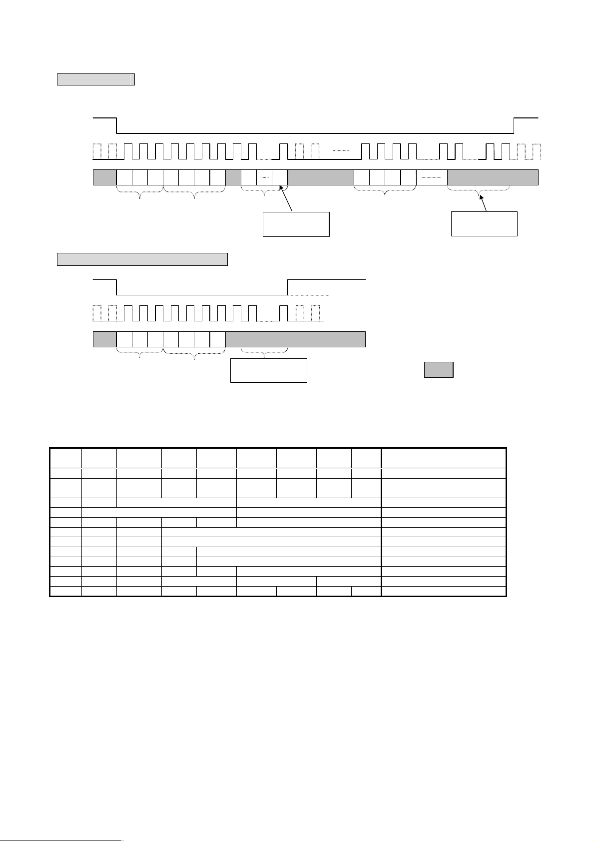
2-2-1 u/A-Law PCM data Mode
8 bits PCM data is accommodated in 1 frame( 125us ) defined by 8kHz frame sync signal.
Although there are 32 time slots at maximum in 8kHz frame(when BCK=2.048MHz), PCM data for AK2307/LV occupies
first time slot as is indicated in figures below.
2-2-1-a Signals
- Frame Sync signal (FS)
8kHz reference signal. This signal indicated the timing and the frame position of 8kHz PCM interface. All the internal
clock
of the LSI is generated based on this FS signal.
- Bit Clock (BCLK)
BCLK defines the PCM data rate. BCLK can be varied from 64kHz to 2.048MHz by 64kHz step.
- PCM data output (DX)
DX is an output signal of 64Kbps PCM u/A-law data. The data is synchronized to the BCLK which determines th e data
rate. The period which the PCM data is not occupied, the DX pin turns to Hi-impedance output. In the long frame mode,
the LSB bit turns to Hi-impedance at the faster edge of ether FS falling edge or 9th rising edge of BCLK.
- PCM data input (DR)
DR is an input signal of 64Kbps PCM u/A-law data. The data is clocked by BCLK at the falling edge and fed into the D/A
block.
2-2-1-b LONG FRAME( LF ) / SHORT FRAME ( SF ) Automatic selection
AK2307/LV monitors the duration of the “H” level of FS and automatically selects LF or SF interface format.
period of FS=”H” Interface format
more than 2 clocks of BCK LF
1 clock of BCK SF
2-2-1-c Frame format of the interface
Long Frame format
FS
BCLK
DX
DR
Short Frame format
FS
BCLK
DX
DR
7 6 5 4 1 03 2
7 6 5 4 1 03 2
care
7 6 5 4 1 03 2
care
7 6 5 4 1 03 2
125us(8KHz)
125us(8KHz)
MS0190-E-05 2005/12
11
ASAHI KASEI [AK2307/LV]
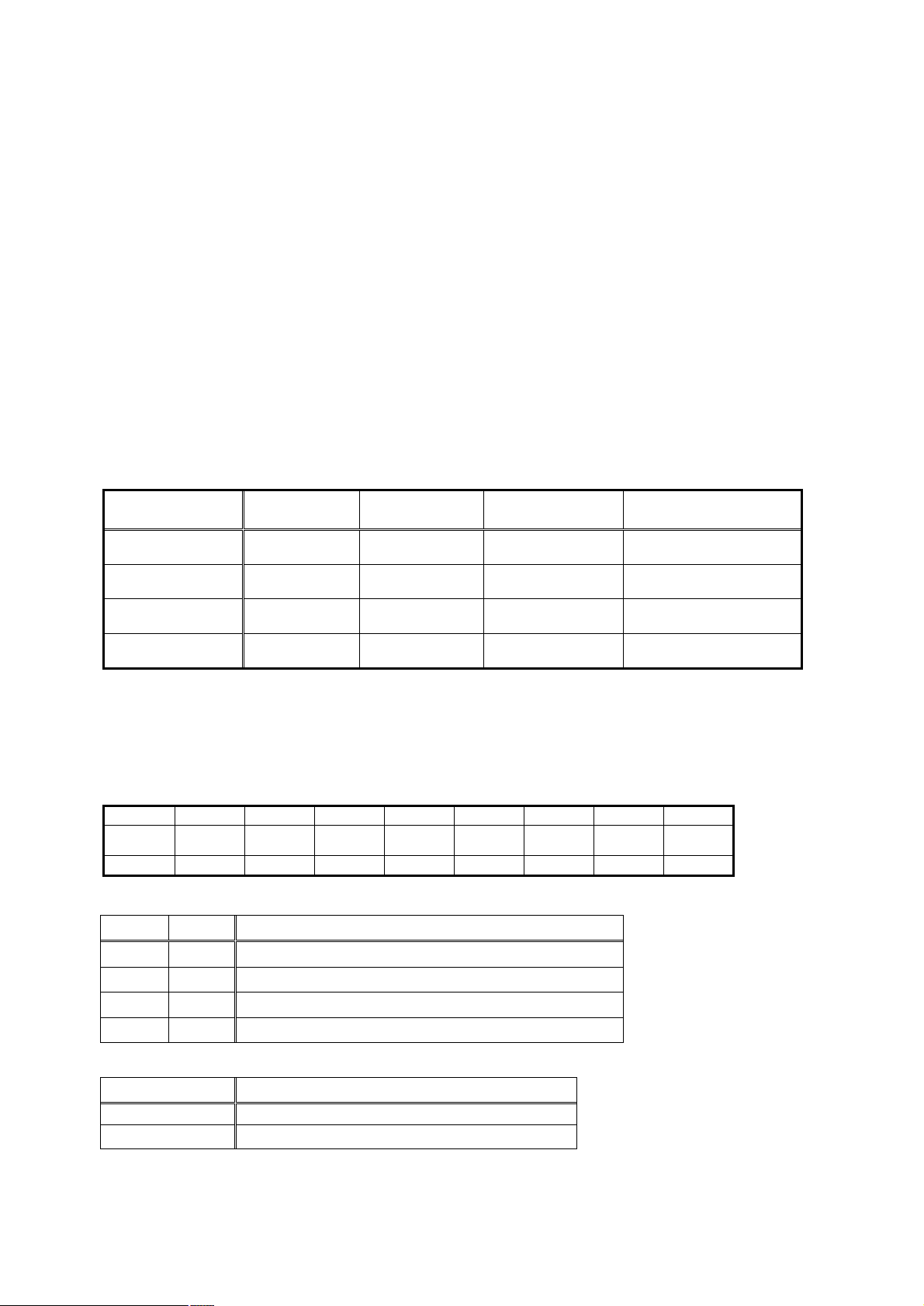
2-2-2 16 bit Linear PCM data mode
In this mode the 16 bit linear PCM data are interfaced to the outside. This mode is useful to compress/extend the PCM
data by much higher compress rate algorithm than u/A-law algorithm by the external DSP. The AK2307/LV CODEC
operates at 14bit accuracy, thus the least 2 bits are output as fixed value.
2-2-2-a Signals
- Frame Sync signal (FS)
8kHz reference signal which is same as in u/A-law PCM data mode. How the FS pulse H level width should be 1 clock
period which is like the short frame FS signal.
- Bit Clock (BCLK)
BCLK defines the PCM data rate. BCLK can be varied from 128kHz to 2.048MHz by 128kHz step which is different
from in the u/A-law PCM data mode.
- PCM data output (DX)
DX is an output signal of 128Kbps linear PCM data. The data is synchronized to the BCLK which determines the data
rate. The period which the PCM data is not occupied, the DX pin turns to Hi-impedance output.
- PCM data input (DR)
DR is an input signal of 128Kbps linear PCM data. The data is clocked by BCLK at the falling edge and fed into the
D/A
block.
16bti Linear Frame format
125us (8KHz)
FS
BCLK
DX
DR
Hi-Z Hi-Z
MSB First
1 2 3
MSB First
1 2 3* *
12 13 14
*12 13 14 *
Hi-Z
* 1
1
2-2-3 AK130 B1/B2 Mode
These modes are for connecting the PCM interface to AK130, AKM’s TCM( ping-pong ) transceiver for PBX/KTS
system.
The PCM data format is A-law or u-law which can be selected by the register. The AK130 B1 mode interfaces the data
to B1 channel which is one of two B channels which AK130 provides, and the AK130 B2 mode interfaces to B2 chann el.
2-2-3-a Signals
- Frame Sync signal (FS) ___
Please feed the FS signal which is generated by AK130.( F0o , pin#3 )
- Bit Clock (BCLK)
BCLK defines the PCM data rate. Please use 2.048MHz clock which is generated by AK130 .( E2o,pin#5 )
- PCM data output (DX)
DX is an output signal of 128Kbps linear PCM data. Please connect to the PCM data input pin of AK130.( DSTi,pin#11 )
- PCM data input (DR)
DR is an input signal of 128Kbps linear PCM data. The data is clocked by BCLK at the falling edge and fed into the
D/A
block. Please connect to the PCM data output pin of AK130.( DSTo,pin#6 )
MS0190-E-05 2005/12
12
 Loading...