


ACM Data Sheet
Version 1.3 Revision 3
November 7, 2013

ACM Data Sheet - November 7, 2013 - Version 1.3 Revision 3
Table of Contents
1 Overview.......................................................................................................................................................3
1.1 Description............................................................................................................................................3
1.2 Benefits.................................................................................................................................................3
1.3 Features................................................................................................................................................4
2 Hardware.......................................................................................................................................................4
2.1 Space Requirements.............................................................................................................................4
2.2 Pinout....................................................................................................................................................5
2.3 Electrical Characteristics......................................................................................................................8
2.4 UART Configuration..............................................................................................................................9
2.5 Antenna...............................................................................................................................................10
3 External Flash and SPI - Usage and Requirements...................................................................................10
4 SKU Nomenclature.....................................................................................................................................11
5 Label Nomenclature....................................................................................................................................11
6 ACM Development Kits and Additional Documentation.............................................................................11
7 FCC NOTICE...............................................................................................................................................12
8 IC NOTICE...................................................................................................................................................12
9 Document Information.................................................................................................................................13
9.1 Document Versioning..........................................................................................................................13
9.2 Revision History...................................................................................................................................14
2
ACM Data Sheet - November 7, 2013 - Version 1.3 Revision 3
1 Overview
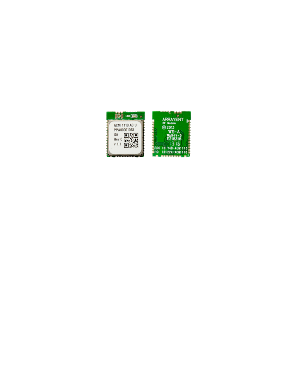
The ACM (“Arrayent Connect Module”, “ACM”, or “Module” for short) is a family of surface-mount modules
for enabling consumer products to communicate wirelessly to the Arrayent Connect Platform, a global
Platform-as-a-Service (PaaS) for connected products.
1.1 Description
The ACM is physically composed of an integrated crystal, internal voltage regulator, matching circuitry,
and filtering. The ACM is based on the CC1110 SoC from Texas Instruments. It measures 0.75 by 0.885
inches and is intended for use as a surface-mount module to be soldered on to the PCB of a consumer
product.
The ACM's energy-aware algorithms support long battery life. When powered by three AA batteries, the
ACM by itself can sustain power for over twelve months.
The ACM has received regulatory approval for modular devices in the United States (FCC), Canada (IC),
and Europe (ETSI).
1.2 Benefits
The ACM has been optimized to connect low-cost consumer products to the Arrayent Connect Platform.
Benefits include:
• Fast time to market
3

ACM Data Sheet - November 7, 2013 - Version 1.3 Revision 3
• Low-power consumption: 2.2uA when sleeping, 165uA when operating normally
• Minimal RF and computer networking experience necessary
• 100% RF-tested in production
• Easy to implement on a two-layer PCB
• Supports whole-house coverage (line of sight range: 150 meters, 10 dBm power output)
• FCC 15.247a2 / 15.249, IC RSS-201 certified
• Compliant with ETSI EN 300 328
1.3 Features
Features of the ACM include:
• 2.3V to 5.5V input
• Three antenna options: external coaxial antenna, wire antenna via through-hole antenna port, and
PCB antenna via ACM pin (PCB antenna option will require additional FCC certification testing)
• Efficient UART interface
• Operates in unlicensed ISM bands (915 MHz in United States, 868MHz in European Union)
2 Hardware
This chapter describes the various hardware requirements and characteristics of the ACM.
2.1 Space Requirements
The ACM is designed to be surface-mounted on a carrier board. The ACM requires 0.75 by 0.855 inches
of space on your carrier board.
4
ACM Data Sheet - November 7, 2013 - Version 1.3 Revision 3
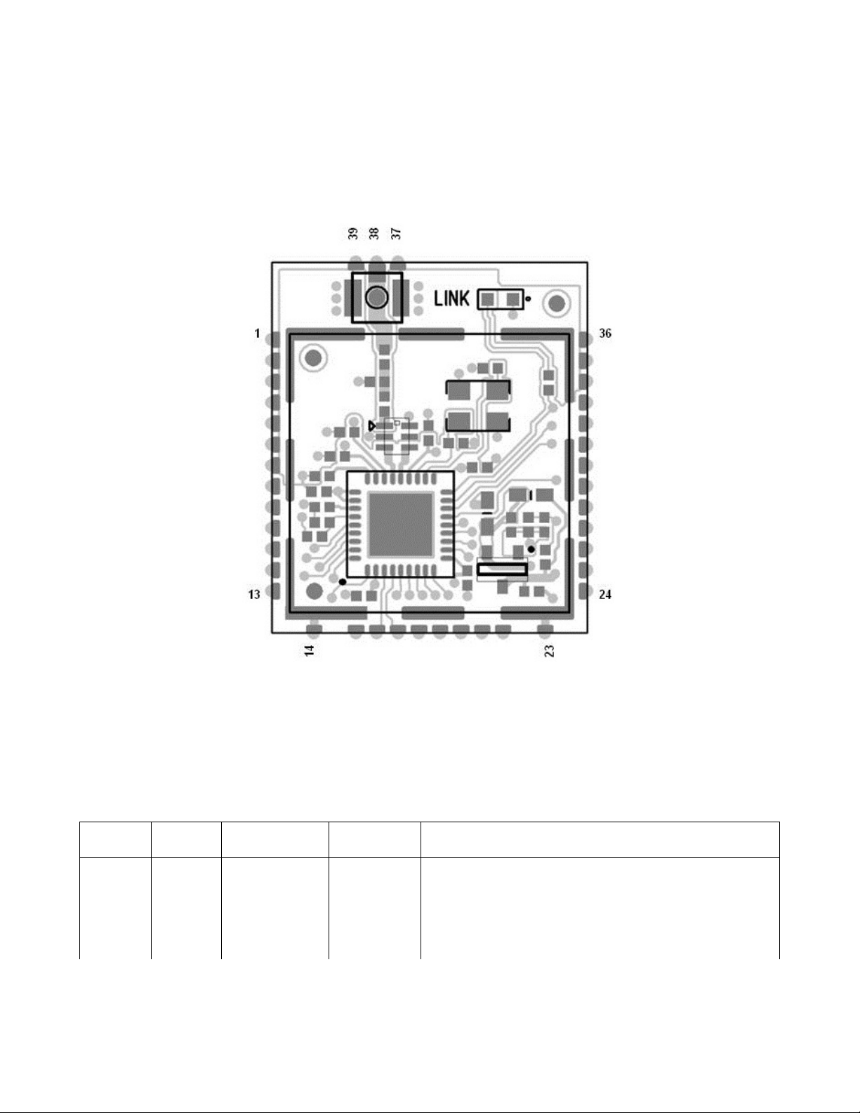
2.2 Pinout
The main interface between the ACM and the Client MCU are the electrical pins of the ACM.
If a pin is not noted in the table below, then it should be considered reserved for internal use and should
not be connected to the circuit of the carrier board.
In the table below, direction is from the perspective of the ACM (input = client MCU ACM, output = →
ACM client MCU).→
Pin # Required Function Direction Description
1-7, 14,
23, 34-
36, 37,
x ACM Ground Connected to carrier board ground. Best practice is
to connect all pins to ground. At minimum, customer
should connect one ground from each corner to
5

ACM Data Sheet - November 7, 2013 - Version 1.3 Revision 3
Pin # Required Function Direction Description
39 ensure good coupling.
20 x SPI_CS_N Output/Hi-Z SPI Select Line. High impedance when SPI_GNT_N
asserted.
21 x SPI_CLK Output/Hi-Z SPI Clock Line. High impedance when SPI_GNT_N
asserted.
22 x SPI_MOSI Output/Hi-Z SPI MOSI Line, for writing data to external flash. High
impedance when SPI_GNT_N asserted.
26 x SPI_MISO Input SPI MISO Line, for reading data from external flash.
17 x SPI_GNT_N Output SPI Grant Line, for arbitrating between multiple
external client MCUs requesting the shared SPI.
16 x SPI_REQ_N Input SPI Request Line, for listening for a request from one
of multiple external client MCUs to control the shared
SPI.
15 x WAKE_N Bidirectional Active low open collector signal, which is driven low
by either the ACM or the client MCU for a preset
period of time before sending any data over the
UART port. 0 = force awake, 1 = allow sleep.
13 ACM_ENABLE Input Active low shutdown line which sends the radio link
of the ACM into a completely inactive state when
driven low. Useful for conserving power. 0 =
disabled, 1 = enabled.
12 x ACM_RX Input UART Rx, for receiving data sent from client MCU.
11 x ACM_TX Output UART Tx, for sending data to client MCU.
6

ACM Data Sheet - November 7, 2013 - Version 1.3 Revision 3
Pin # Required Function Direction Description
9 x ACM_CCA Input Input to the ACM that allows or disallows the ACM
from transmitting on its radio channel. When
asserted by the Client MCU, the ACM will delay data
transmission until the Client MCU releases the signal.
Useful in a multi-radio environment for avoiding
traffic collisions. 1 = RF busy, 0 = OK for ACM to
transmit.
33 STATUS_LED Output Active high output pin which controls the ACM's
LED.
8 RESET_N Input Active low output pin which forces a hard reboot of
the ACM.
25 x ACM Power In Input voltage to ACM. 2.3 to 5V DC.
24 ACM Power
Output
Output voltage from ACM. Customers may use VOUT
as an external power source for SPI flash.
7

ACM Data Sheet - November 7, 2013 - Version 1.3 Revision 3
2.3 Electrical Characteristics
The ACM includes an internal voltage regulator supplied through one of the module pins. Power is
sourced from the customer carrier board and must comply with the following characteristics:
Net Min Typ Max Description
V
input
V
output
I
pm2
I
idle
I
rx
2.3 3.6V 5.5 Internal voltage, regulated to 3.3V
maximum.
3.3V ACM output voltage. Follows VIN up to a
maximum of 3.3V. Maximum current is
50mA.
2.2uA Sleep.
4.1mA Idle.
22mA Receive.
8

ACM Data Sheet - November 7, 2013 - Version 1.3 Revision 3
Net Min Typ Max Description
I
tx
I
average
35mA Transmit at 10dBm.
165uA Average total when ACM is operating in a
normal connected state.
l
average
is the average value during connected operation assuming that the ACM receives one message
every ten minutes. In this state, the ACM is online and is available to send and receive messages in both
directions (from the Client MCU to the Arrayent Cloud, and vice versa).
2.4 UART Configuration
The following table represents the default UART configuration of the ACM.
Parameter Default Value Configurable
Baud Rate 38400. All standard rates from
2400 to 115200 are supported.
Yes
Data Bits 8 No
Parity None No
Stop Bits 1 No
Flow Control None No
Wake Delay 1. Range of supported values is 1
Yes
ms to 255 ms.
Wake Delay refers to the number of milliseconds the ACM will wait after it drives the wake pin low before
sending data to the Client MCU.
The baud rate of the ACM can be adjusted to meet the needs of your product.
9

ACM Data Sheet - November 7, 2013 - Version 1.3 Revision 3
2.5 Antenna
The ACM supports three antenna options:
1. Coaxial external antenna connected to optional U.FL connector
2. Low-cost wire antenna, soldered to the ACM's through-hole antenna port
3. PCB or chip antennas attached to carrier board, connected to RF pin on ACM. Note that this
option will require additionall FCC certification testing.
Antenna requirements are dictated by the System-on-Chip driving the ACM, the Texas Instruments
CC1110. Read more about antenna recommendations for the CC1110 at:
http://www.ti.com/lit/an/swra367a/swra367a.pdf
3 External Flash and SPI - Usage and Requirements
The ACM requires access to an external flash memory chip via a shared SPI bus. The shared SPI bus and
external flash are used for two purposes:
1. Storing ACM firmware images
2. Storing Client MCU firmware images and data when the ACM performs over-the-air downloads
The flash chip must be segmented into a series of contiguous address ranges, called “slots”. The
minimum size for each slot is 64KB. The external flash memory chip must support partial page
programming. Compatible models include (but are not limited to):
• Macronix
• Winbond
• Spansion
10

ACM Data Sheet - November 7, 2013 - Version 1.3 Revision 3
4 SKU Nomenclature
ACM-110-900 (Arrayent Connect Module, TI CC1110, 915MHz without coax)
ACM-110-910 (Arrayent Connect Module, TI CC1110, 915MHz with coax)
ACM-110-800 (Arrayent Connect Module, TI CC1110, 868MHz without coax)
ACM-110-810 (Arrayent Connect Module, TI CC1110, 868MHz with coax)
5 Label Nomenclature
The QR Code evaluates to the following string (excluding quotes): “<Device Name>-<Device Password>”.
6 ACM Development Kits and Additional Documentation
Contact info@arrayent.com to purchase an ACM Development Kit (“DevKit”). The DevKit will give you
access to the ACM Developer Guide, which is the definitive guide for learning how to implement a
connected product that interfaces with the ACM.
11

ACM Data Sheet - November 7, 2013 - Version 1.3 Revision 3
7 FCC NOTICE
FCC ID: Y4B-ACM1110
This device complies with part 15 of the FCC Rules. Operation is subject to the following two conditions: (1) This device may not cause
harmful interference, and (2) this device must accept any interference received, including interference that may cause undesired operation.
This equipment has been tested and found to comply with the limits for a Class B digital device, pursuant to part 15 of the FCC Rules. These
limits are designed to provide reasonable protection against harmful interference in a residential installation. This equipment generates, uses,
and can radiate radio frequency energy and, if not installed and used in accordance with the instructions, may cause harmful interference to
radio communications. However, there is no guarantee that interference will not occur in a particular installation. If this equipment does cause
harmful interference to radio or television reception, which can be determined by turning the equipment off and on, the user is encouraged to
try to correct the interference by one or more of the following measures:
• Reorient or relocate the receiving antenna
• Increase the separation between the equipment and receiver
• Connect the equipment into an outlet on a circuit different from that to which the receiver is connected
• Consult the dealer or an experienced radio/TV technician for help
The FCC requires the user to be notified that any changes or modifications made to this device that are not expressly approved by Arrayent,
Inc., may void the user's authority to operate the equipment.
To comply with FCC RF exposure compliance requirements, the antenna used for this transmitter must be installed to provide a separation
distance of at least 20 cm from all persons and must not be co-located or operating in conjunction with any other antenna or transmitter.
This equipment is sold only to OEM integrators and must be installed by the OEM or OEM integrators under the following conditions:
• The antennas used for this transmitter must be installed to provide a separation distance of at least 20 cm from all persons, and
• The transmitter must not be co-located with any other antenna or transmitter.
8 IC NOTICE
IC ID: 10122A-ACM1110
English
This device complies with Industry Canada licence-exempt RSS standard(s). Operation is subject to the following two conditions:
• this device may not cause interference, and
12

ACM Data Sheet - November 7, 2013 - Version 1.3 Revision 3
• this device must accept any interference, including interference that may cause undesired operation of the device.
This product meets the applicable Industry Canada technical specifications.
The Class [B] digital apparatus meets all requirements of the Canadian Interference-Causing Equipment Regulation.
French
Cet appareil est conforme à Industrie Canada une licence standard RSS exonérés (s). Son fonctionnement est soumis aux deux conditions
suivantes:
• Cet appareil ne doit pas provoquer d'interférences
• Cet appareil doit accepter toute interférence reçue, y compris les interférences pouvant provoquer un fonctionnement indésirable
de l'appareil.
Ce produit est conforme aux spécifications d'Industrie Canada.
La classe [B] appareil numérique est conforme à toutes les exigences du règlement équipement brouilleur du Canada.
9 Document Information
This chapter contains information about the data sheet document itself.
9.1 Document Versioning
The title page and header of this document contains versioning information in the form of “Version X.x
Revision X”.
“Version” represents the version of the ACM product which this document corresponds to. Make sure that
the “Version” corresponds to the version of the ACM which you are developing upon, as newer versions of
the ACM may contain features not supported in older versions of the ACM.
“Revision” represents the number of revisions made to this document for this version of the ACM. The
document with the highest revision number for each respective ACM version is the most up to date.
13

ACM Data Sheet - November 7, 2013 - Version 1.3 Revision 3
9.2 Revision History
Date Revision Description
7 November 2013 3 Updated FCC and IC notices.
Added note that using ACM with PCB antenna requires
additional FCC certification testing.
21 October 2013 2 Expanded description of l
in Section 2.3 “Electrical
average
Characteristics“ to define “normal operating state”.
17 October 2013 1 Note that the ACM Data Sheet has been in circulation but
was not properly revisioned. Revisions below are changes
made from the most recent, un-revisioned Data Sheet.
Removed ACM software block diagram from Section 1.1
“Description“.
Changed the pinout numbering scheme in the diagram and
table of Section 2.2 “Pinout“. Previously, pins were labeled
according to their CC1110 mapping. Now, pins are linearly
labeled from 1 to 39, counterclockwise from top left.
Added information about range of supported Baud rates and
wake delay in Section 2.4 “UART Configuration“.
Added description of VOUT to Section 2.2 “Pinout“ and
Section 2.3 “Electrical Characteristics“.
Reduced font size of FCC and IC Chapters.
Added Chapter 5 “Label Nomenclature“.
Updated Chapter 4 “SKU Nomenclature“ to reflect new
naming scheme.
14
 Loading...