

Page 1
·
~-.~
..
~
.. "
~.,",:.
>
tme'
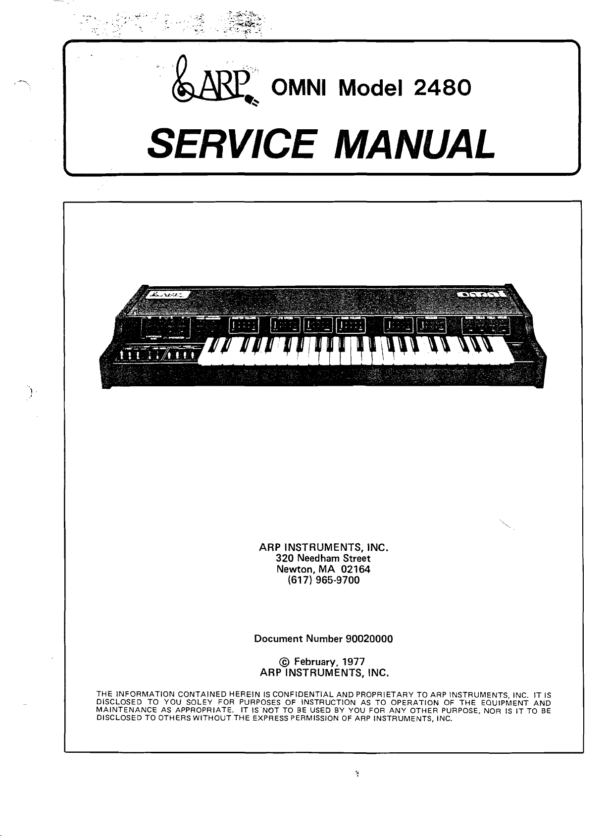
OMNI
Model
2480
.~
SERVICE MANUAL
THE
INFORMATION
DISCLOSED
MAINTENANCE
DISCLOSED
TO
TO
AS
OTHERS
YOU
CONTAINED
SOLEY
APPROPRIATE.
FOR PURPOSES OF
WITHOUT
ARP INSTRUMENTS, INC.
Needham
320
Newton,
MA
(617) 965-9700
Document Number 90020000
© February, 1977
ARP INSTRUMENTS, INC.
HEREIN
THE
IS
CONFIDENTIAL
IT
IS
NOT
EXPRESS PERMISSION OF ARP
INSTRUCTION
TO
BE USED BY
AND
Street
02164
PROPRIETARY
AS
TO
YOU
FOR
INSTRUMENTS,
TO
OPERATION
ANY
OTHER
ARP
INSTRUMENTS,
OF
THE
PURPOSE,
INC.
NOR
IS
INC.
IT
EQUIPMENT
TO
IT
AND
BE
IS
Page 2
OMNI Model
2480
SERVICE MANUAL
TABLE
1.
INTRODUCTION
1.1
Product Description 2
1.2 Specifications 2
1.3
Function
2.
THEORY
3.
CIRCUIT
3.1
Upper
Lower
3.2
3.3 String
3.4 Synthesizer
3.5 Synthesizer Board 10
3.6
Phaser
3.7 Power Supply
4.
ASSEMBLy/DiSASSEMBLy
5.
GENERAL
6.
CALIBRATIONS
SCHEMATICS & LAYOUTS
7.
Description 3
OF
OPERATION
DESCRIPTIONS
Voicing
Voicing
Control
Control
Board 10
INFORMATION
OF
CONTENTS
Board 5
Board 6
Board 8
Board 9
5
11
12
12
13
14-33
8. PARTS
LIST
34-36
1
Page 3
SECTION 1
INTRODUCTION
1.1
Product Description
The
ARP
OMNI
offers
polyphonic
sizer
synthesizer
sounds
synthesizer
piano,
The
by
stereo
ARP's
this
effects
The
and
tone
sources
sound
string
product
computer-grade
reliable.
modification.
sections
simultaneously.
section
and
clavi
net
and
synthesizer
outputs
now-famous
as well.
or
output
its
1.2 Specifications
I.
Controls
A.
String
Section
1.
Instrument
a.
Violins
b.
Violas
c. Cellos
d.
Bass
2.
String
a.
Attack
b. Release
B.
Synthesizer
1.
Synthesizer
a. 4'and
2.
Synthesizer
a.
8'
3.
Voltage
a.
VCF
b.
Resonance
c.
ADSR
d.
LFO
e. Pedal &
4.
LFO
Speed
5.
Synthesizer
a.
Sawtooth
b.
Dynamic
6.
ADSR
a.
Attack
b.
Decay
c.
Sustain
d. Release
C.
General
Controls
the
and
allow
The
permits
without
on
the
systems
The
own
signals
switching
Selection
(4')
(8')
(8')
(16')
Envelope
Time
Time
Section
Waveform
8'
Bass
and
16'
Controlled
Freq
depth
depth
Acc.
Slider
Waveforms
Time
Time
Level
Time
unique
the
versatility
Separate
orchestral
total
such
single
sections
rear panel
interface
OMNI
can
tv
mechanisms
Controls
Switches
Filter
depth
Pulse
combination
string
and
symphonic
variability
sounds
note
limitations.
may
be
of
accept
other
instruments.
Switches
Switches
of
synthe-
of
as brass,
separated
the
OM NI.
applies
external
are
of
and
the
to
fast
1. Master
2. Bass
3.
4.
5.
II.
Outputs
- A. Main
1_
2.
'--
B.
Synthesizer
1.
--"Can
stereo
C.
Gate
1.
2. Trigger:
D.
Foot
1.
III.
Miscellaneous
A.
Keyboard
1. 4
B.
Pedals
1.
Sustain
C.
1.
D.
Materials
1.
2. Rigid
3.
4. Glass-epoxy
5.
E.
Weight
1.
Volume
Volume
String/SYnthesizer
Waveform
Synthesizer-to-Modulator
Outputs
High Level
Low
Low
be used
effects.
Out
Gate:
2 microsec.
Switch
Standard
octave
at
Filter
filter
Foot
piano
Aluminum
Solid
Industrial-grade
and
33
RMS
TYP.
Level
RMS
TYP.
Output
Level
TYP.
and
Trig
Tini D
Tini D Jack;
and
ARP
one
and a half
control
brightness
Switch
switch
high-density
walnut
controls
pounds
Enhancement
Cannon
1/4"
simultaneously
keyboard,
phone
1/4"
phone
Out
Jack;
duration
Foot
accessories
pedal
works
chassis
end
blocks
circuit
electronic
Mix
XLR, 1K,
0,
+1
Pedal
split
octaves
for
like
particle
boards
Switch
Switch
1OK,
10K,
for
OV
0,
+10V
for
from
foot
sustain
board
components
2.5V
.8V
.8V
discreet
bass
low
co~1
pedal
base
RMS
pulse,
voices
end
of
.
on
2
Page 4
3 2
16
17
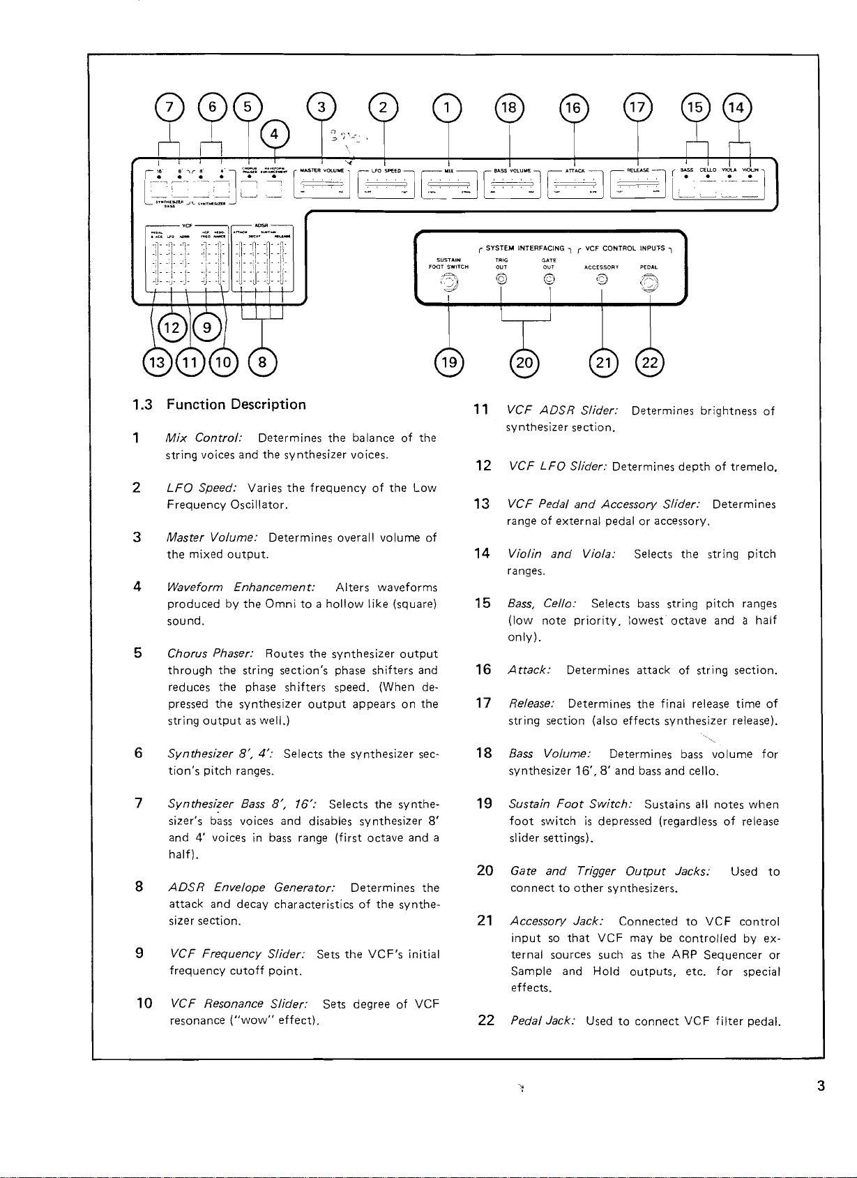
1.3
Function Description
Mix Control:
1
string
voices
LFO Speed: Varies
2
Frequency
Master Volume:
3
the
Waveform Enhancement:
4
produced
sound.
Chorus Phaser:
5
through
reduces
pressed
string
mixed
output
Oscillator.
output.
by
the
the
the
Determines
and
the
synthesizer
the
Determines
the
Omni
Routes
string
section's
phase
shifters
synthesizer
as well.)
the
balance
voices.
frequency
overall
Alters
to a hollow
the
synthesizer
phase
speed.
output
appears
FOOT
of
the
of
the
Low
volume
waveforms
like (square)
shifters
(When de-
of
output
and
on
the
r SYSTEM INTERFACING I r VCF CONTROL
SUSTAIN
SWITCH
TRIG
OUT
11
VCF
synthesizer
12
VCF LFO Slider:
GATE
ou'
ADSR
13 VCF Pedal
range
of
14 Violin
ranges.
15 Bass, Cello:
(low
note
only).
Attack:
16
17 Release:
string
section.
and
external
and
priority,
Determines
Determines
section
INPU1=S
ACCESSORY PEDAL
21
Slider:
22
Determines
Determines
Accessory Slider:
pedal
or
Viola:
Selects
(also
Selects
bass
lowest
attack
the
effects
I
brightness
depth
accessory.
the
string
string
pitch
octave
of
string
final release
synthesizer
of
of
tremelo.
Determines
pitch
ranges
a
and
half
section.
time
release).
of
Synthesizer
6
tion's
pitch
7
Synthes/~er
8
9
10
sizer's
and
ADSR
bass voices
4'
voices
half).
Envelope Generator:
attack
and
sizer
section.
VCF Frequency Slider:
frequency
VCF Resonance Slider:
resonance
8',
4':
ranges.
Bass
in
decay
cutoff
("wow"
Selects
8',
and
bass range
characteristics
point.
effect).
16':
disables
Sets
the
Selects
Sets
synthesizer
synthesizer
(first
octave
Determines
of
the
VCF's
degree
the
the
sec·
synthe-
and
synthe-
initial
of
VCF
8'
the
18
Bass Volume:
synthesizer
Sustain
19
foot
a
slider
20
Gate
connect
21
Accessory Jack:
input
ternal
Sample
effects.
Pedal Jack: Used
22
Foot
switch
settings).
and
to
so
that
sources
and
16',8'
Switch:
is
depressed
Trigger
other
VCF
such
Hold
Determines
and
bass
and
Sustains
(regardless
Output
synthesizers.
Connected
may
be
as
the
outputs,
to
connect
bass
cello.
all
Jacks:
to
VCF
controlled
ARP
Sequencer
etc.
VCF
volume
notes
of
release
Used
control
for
special
filter
for
when
by
ex-
pedal.
to
or
3
Page 5

~
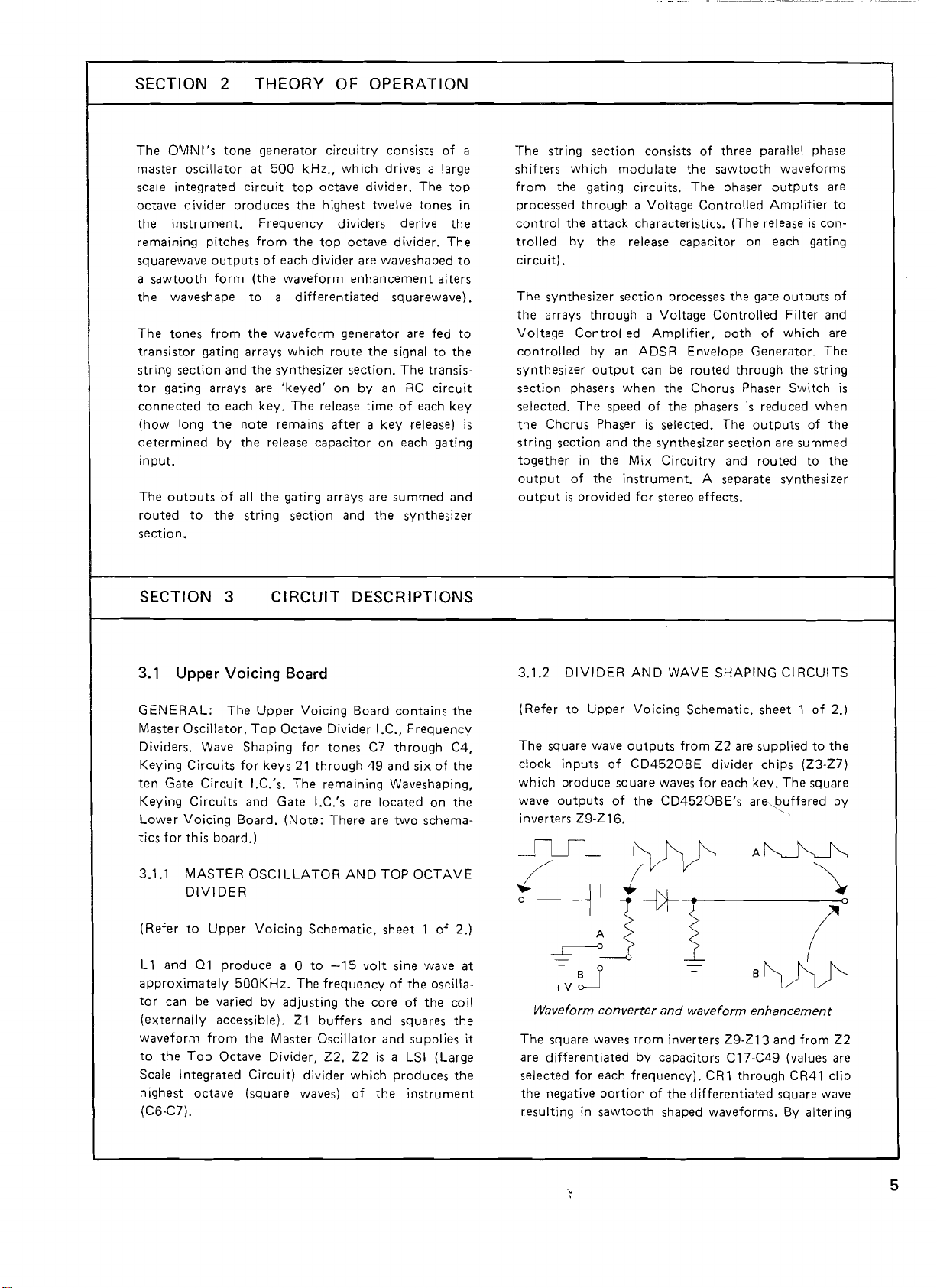
MASTER
OSCILLATOR
1 line
TOP
OCTAVE
DIVIDER
SIMPLIFIED OMNI BLOCK
..rt...rL ..rt...rL
12
lines
FREOUENCY
DIVIDERS
~
49
lines
WAVE
SHAPERS
BUS
RODS
BASS
I L
..rt...rL
2.!.J.ines
L.-.t..
DIAGRAM
GATE
CIRCUITS
t
49
lines
KEYING
CIRCUITS
21 lines
~
BASS
PRIORITY
CIRCUIT
t
4'
-
8'
-
8'
~
16'
~
1-----------------
I
--+--
PHASER
f-----
~
t t
STRING
-...:z::.
chorus
r--
I
AR
SECTION
switch
I
r-
STRING
----------------~
r---------------~
I
I
~
VCF
I
I
t
STRING
VCA
I
VCA
t
~
I
I
I
:
I
~
,------.
OUTPUT
M/X
MIX
OUTPUT
SYNTH
OUTPUT
,;'"
0
ESIZER
/
SYNTHESIZER
L
ADSR
SECTION
~
Page 6
SECTION
The
OMN I
master
scale
octave
the
remaining
squarewave
a
the
The
transistor
string
tor
connected
(how
determined
input.
The
routed
section.
oscillator
integrated
divider
instrument.
sawtooth
waveshape
tones
section
gating
long
outputs
to
2
's
tone
pitches
outputs
form
from
gating
and
arrays
to
each
the
by
of
the
THEORY
generator
at
500
circuit
produces
Frequency
from
of
(the
to
a
the
waveform
arrays
the
synthesizer
are
key.
note
remains
the
release
all
the
string
circuitry
kHz.,
top
octave
the
highest
the
top
each
divider
waveform
differentiated
which
route
'keyed'
gating
The
release
capacitor
section
on
after a key
arrays
OF
OPERATION
consists
which
drives a large
divider.
twelve
dividers
octave
are
waveshaped
enhancement
generator
the
section.
by
an
time
on
are
and
the
of
The
top
tones
in
derive
divider.
squarewave).
signal
The
of
each
summed
synthesizer
alters
are fed
to
transis-
RC
circuit
each
release)
gating
the
The
to
to
the
key
and
a
is
The
string
shifters
from
the
processed
control
trolled
circuit).
The
the
Voltage
controlled
synthesizer
section
selected.
the
string
together
output
output
the
by
synthesizer
arrays
Chorus
section
is
section
which
gating
through a Voltage
attack
the
through a Voltage
Controlled
by an
output
phasers
The
Phaser
in
of
the
provided
consists
modulate
circuits.
characteristics.
release
section
Amplifier,
ADSR
can
when
the
speed
of
is
selected.
and
the
synthesizer
the
Mix
Circuitry
instrument. A separate
for
stereo
of
the
sawtooth
The
Controlled
capacitor
processes
Controlled
Envelope
be
routed
Chorus
the
phasers
effects.
three
phaser
(The
the
both
through
Phaser
is
The
section
and
parallel
waveforms
outputs
Amplifier
release
on
each
gate
outputs
Filter
of
which
Generator.
the
Switch
reduced
outputs
are
routed
synthesizer
phase
are
to
is
con-
gating
of
and
are
The
string
when
of
the
summed
to
the
is
SECTION
3
CIRCUIT
3.1 Upper Voicing Board
GENERAL:
Master
Dividers, Wave
Keying
ten
Gate
Keying
Lower
tics
for
3.1.1
(Refer
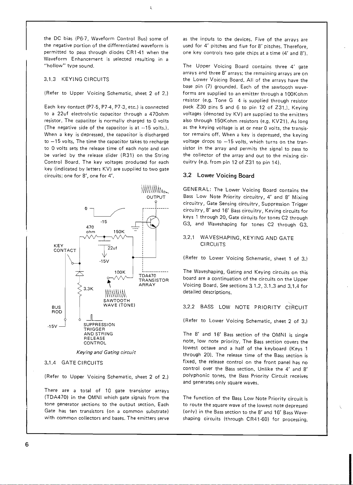
L1
and
approximately
tor
can
(externally
waveform
to
the
Scale
Integrated
highest
(C6·C7).
The
Oscillator,
Circuits
Circuit
Circuits
Voicing
th
is
board.)
MASTER
DIVIDER
to
Upper
01
produce
500KHz.
be varied
accessible).
from
Top
Octave
octave
Upper
Top
Shaping
for
keys
/.C.'s.
and
Board.
OSCI
Voicing
by
the
Master
Divider,
Circuit)
(square
Voicing
Octave
for
21
through
The
Gate
I.C.'s are
(Note:
LLATOR
Schematic,
a 0
to
The
adjusting
Z1
divider
waves)
DESCRIPTIONS
Board
contains
Divider I.C.,
tones
C7
through
49
and
remaining
There
-15
frequency
the
buffers
Oscillator
Z2.
AND
volt
Z2
which
of
are
core
and
is
the
Waveshaping,
located
two
TOP
sheet 1 of
sine
of
and
a LSI
produces
Frequency
six
of
on
schema-
OCTAVE
wave
the
oscilla-
of
the
squares
supplies
(Large
instrument
the
C4,
the
the
2.)
at
coil
the
the
3.1.2
The
o
(Refer
square
clock
inputs
which
produce
wave
outputs
inverters
DIVIDER
to
Upper
wave
of
of
Z9-Z16.
AND
Voicing
outputs
CD4520BE
square
waves
the
WAVE
SHAPING
Schematic,
from
Z2
divider
for
each
CD4520BE's
CIRCUITS
sheet 1 of
are
supplied
chips
key.
The
are~uffered
2.)
to
the
(Z3-Zl)
square
by
i
Waveform
it
The
square
are
differentiated
selected
the
negative
resulting
converter
waves Trom
for
each
portion
in
sawtooth
and
waveform
inverters
by
capacitors
frequency).
of
the
shaped
enhancement
Z9·Z13
C17-C49
CR1
through
differentiated
waveforms.
and
from
(values are
CR41
square
By
altering
Z2
clip
wave
5
Page 7
the
DC
bias (P6-7,
the
negative
permitted
Waveform
"hollow"
3.1.3
(Refer
Each
to a 22uf
resistor.
(The
When a key
to
-15
to
0 volts sets
be varied by
Control
key
circuits;
to
type
KEY I
to
Upper
key
contact
The
negative
volts.
Board.
(indicated
one
Waveform
portion
Enhancement
NG
electrolytic
for
pass
through
sound.
CI
RCUITS
Voicing
(P7-5, P7-4,
capacitor
side
of
is
depressed,
The
time
the
release
the
release slider
The
by
letters
8',
one
of
key
the
differentiated
diodes
is
Schematic,
capacitor
is
normally
the
capacitor
the
the
capacitor
time
voltages
KV) are
for
4'.
Control
selected
P7-3,
capacitor
of
(R31)
Bus)
waveform
CR1-41
resulting in a
sheet 2 of
etc.)
is
through a 4700hm
charged
is
at
-15
is
takes
each
note
on
produced
supplied
some
when
the
connected
to 0 volts
volts.).
discharged
to
recharge
and
can
the
String
for
each
to
two
gate
of
2.)
as
the
inputs
to
the
devices. Five
is
for
4'
used
one
key
controls
The
Upper
arrays
and
the
Lower
base pin (7)
forms
are
supplied
resistor
pack
voltages
also
as
tor
voltage
sistor
the
cuitry
Z30
through
the
keying
remains
in
collector
(e.g.
(e.g.
(denoted
drops
the
pitches
three
Voicing Board. All
pins 5
from
and five
two
Voicing Board
8'
arrays;
grounded.
to
Tone
G 4
and 6 to
by KV)
150Kohm
voltage
off.
When a
to
-15
array
and
of
the
array
pin 12
3.2 Lower Voicing
gate
chips
the
Each
an
emitter
is
supplied
are
resistors (e.g.
is
at
or
key
volts,
permits
and
of
Z31
Board
of
the
for
8'
pitches.
at a time
contains
remaining
of
of
pin
supplied
near
is
depressed,
which
out
to
three
arrays
the
arrays
the
sawtooth
through a 100Kohm
through
12
of
Z31.).
to
the
KV21).
0 volts,
turns
on
the
signal
to
the
pin
14).
arrays
are
Therefore,
(4'
and
8').
4'
gate
are
have
the
wave-
resistor
Keying
emitters
As long
the
transis-
the
keying
the
tran-
to
pass
mixing
cir-
on
to
KEY
CONTACT
BUS
ROD
-15V
3.1.4
GATE
(Refer
There
(TDA470)
tone
Gate
with
to
are a total
generator
has
common
Keying
CI
Upper
in
the
ten
collectors
sections
transistors
-15
470
ohm
,
3.3K
~~WmJi
SAWTOOTH
WAVE
_IL
SUPPRESSION
TRIGGER
AND
STRING
RELEASE
CONTROL
and
Gating circuit
RCUITS
Voicing
OMNI
Schematic,
of
10
which
to
the
(on a common
and
150K
100K
(TONE)
gate
gate
output
bases.
TDA470
TRANSISTOR
ARRAY
sheet 2 of
transistor
signals
section.
The
emitters
OUTPUT
,
,
,
,
,
~-------
arrays
from
substrate)
-
----
2.)
the
Each
serve
GENERAL:
Bass
Low
circuitry,
circuitry,
keys 1
through
G3,
and
3.2.1
The
Voicing
detailed
3.2.2
The
through
fixed,
control
polyphonic
and
The
to
shaping
WAVESHAPING,
CI
(Refer
board
(Refer
note,
lowest
(only) in
to
Waveshaping,
are a continuation
Board. See
descriptions.
BASS LOW
to
8'
and
low
octave
20).
the
over
generates
function
route
the
the
circuits
The
Lower
Note
Priority
Gate
Sensing
8'
and
16'
20,
Gate
Waveshaping
RCUITS
Lower
Voicing
Gating
sections 3 1.2,
Lower
Voicing
16'
Bass
note
priority.
and
a half
The
release
release
the
tones,
only
of
the
square
Bass
control
Bass
the
square
wave
section
(through
circuitry,
Bass
NOTE
section
section.
Bass
Bass
Voicing
circuitry,
circuitry,
circuits
for
tones
KEYING
Schematic,
and
Keying
of
the
PRIORITY
Schematic,
of
The
Bass
of
the
time
on
the
Priority
waves.
Low
Note
of
the
lowest
to
the
CR41-60)
Board
4'
and
Suppression
Keying
for
tones
C2
AND
sheet 1 of
circuits
circuits
of
Unlike
8'
3.1.3
sheet 2 of
the
OMN I
section
keyboard
the
Bass
front
the
Circuit
Priority
note
and
16'
for
on
contains
8'
Mixing
Trigger
circuits
C2
through
through
GATE
on
the
Upper
and
3.1.4
CIRCUIT
is
covers
(Keys
section
panel
has no
4'
and
receives
circuit
depressed
Bass Wave-
processing.
the
for
G3.
3.)
this
for
3.)
single
the
1
is
8'
is
6
I
Page 8

The
may
Bass
Waveshaping
only
accept
one
circuits
waveform
are
monophonic;
at a time.
they
(Z33-Z47)
keys
higher
to
than
transmit
the
one
serially a logic 1
depressed.
state
to
all
Square
Voicing
three
outputs
only
Z33B
are
NOTE:
section are COSMOS (Complimentary
wave
tones
Board
frequency
input
nor
of
these
when
the
pin 6 is a square
at
logic
0.).
All
logic gates in the Bass
C2-G3
gate
nor
other
for
gates
two
wave
are
routed
dividers
each
are
inverted
inputs
only
from
the
Upper
to
one
input
key
(Z33-Z39).
square
waves
are a logic 0 (e.g.
if
pin 4
and
Low
Note
Priority
Symmetry
of
The
pin 3
Metal Oxide Semiconductor) devices. For this
they
particular application,
ground
voltage
voltage
and
-15
between
between
volts. Therefore, a logic 1
ground
-7.5
~
------I~
~~I-----i-
6
,
(A)
I
ENABLE
6
KEYING
The
only
and
The
Z33B,
provided
circuit
(B)
VOLTAGE
output
(C)
of
the
when the Enable (A)
when
the Keying voltage is less than -7.5V.
"enable"
pin
no
under
input
of
3)
will
always
keys
are
examination.
are operated
and
-7.5
volts, logic 0
volts
and
-15
volts.
LJLJ
!
~
NOR
gate will
the
three
depressed
<)
be
input
is a logic 0 (-15V)
input
be
a logic 0
to
between
is
is
--0
a square wave
nor
gates
(-15
volts)
the
left
of
any
any
(e.g.
the
(C)
ENABLE
(C)
a
0-------------,
KEYING
VOLTAGE
(B)
0------1
Enable (A) is a logic 0
Keying voltage is less than
The
release
is
fixed
charge
not
depressed
keys are
of
01-20
keying
3.2.3
(Refer
The T point
supplies a voltage
Low
diode
to
the
drops
insures
bus
depressed.
3.2.4
(Refer
at
about
path
depressed,
is
(bus rod)
BASS
to
Lower
Note
drops
Lower
are
created
that
voltage
GATE
to
Lower
time
(decay
2.5
seconds,
is
provided
to
shorten
01-20
always
of
Priority
higher
01-20
held
voltage
KEYING
Voicing
the
Bass Keying
to
the
Circuit
than
keyboard
using CR
will be biased ON regardless
wh
ich
decreases
DETECTOR
Voicing
only
when Enable
-7.5V
(logic 0). -
time
after
however,
through
VOLTAGE
the
release
are
off.
a full
diode
in
the
Schematic,
bass
of
which
the
keying
bus
rod
114,
030
CIRCUITS
Schematic,
01-20
ENABLE
)-------e
(C)
keys
are
released)
an
additional
for
those
time.
When
The
base
drop
above
reference
Reference
01-20
(P1·14).
as
generator.
sheet 3 of
Generator
of
is
at
least
voltage
The
andCR113.This
more
keys
sheet 3 of
(A)
and
the
keys
no
voltage
the
3.)
the
Bass
three
supplied
diode
of
the
are
3.)
When a key
discharges
transistors
C42
through
depression.)
the
capacitor
through a 3.3Mohm
voltage
gates
permits
input
provided
volts
no
lower
The
keying
COSMOS
is
(e.g.
the
of
that
and
keys
is
depressed,
a 1
uf
(01-020).
R7,
02
When a key
is
allowed
routed
the
B)
Z33B,
square
three
A)
the
are being
voltage
inverter
to
the
enable
sustain
(e.g. Key
and
resistor
an
pin
4).
wave
input
keying
played).
is
(Z45-Z47)
-15
capacitor
CR63
is
released,
to
charge
input
Thus
to
be
nor
voltage
input
also
volts
from
through
2,
Pl-12
to
-15
the
back
(e.g.
R5).
of
the
three
the
keying
transmitted
gate
to
is
is
a logic 0
processed
and
the
discharges
volts
voltage
to
This
input
from
the
less
than
(indicating
through
a
nor
bus
rod
keying
on
key
on
0 volts
keying
nor
voltage
the
output
-7.5
gate
There
are
two
bus
rods
in
the
OMN
I,
one
for
the
lowest
20
keys,
one
for
the
upper
29
keys. Spl itti ng
the
bus
rod
in
this
manner
(Bass
AR)
to
be
developed
keys.
CR107
source
through
is
volts
R130
across R
differentiated
comparator
a
volts
duration,
(Upper
for
CR107
depressed,
to
ground
on
key
130.
to
-15
Bass
the
upper
and
comparator
(Gate).
depression
The
by
Z52A
volts
longer
R130
voltage
C86
momentarily
and
for
separately
Gate
Detector)
bus
rod.
to
Z52B
The
results
so
back
multi-key
permits
-15
the
bus
switches
current
change
that
switches
again
depressions).
a bass
envelope
from
the
is
the
volts
is
suppl
rod.
When a key
from
drawn
in a voltage
across R
the
through
output
from
(10ms.
higher
voltage
ied
-15
drop
130
is
of
+15
typical
This
7
Page 9
pulse
is
used
for
triggering
(ADSR)
not
3.2.5
(Refer
The
Priority
gated
and
when
when a key
C R1
Z51 A.
amplitude
couples
and
022).
same (+7V).
rising edge
clipping
sawtooth
down
synthesizer
and
signal.
8'
in
for
provided
3.2.6
(Refer
The
clipping
key.
waveforms
+15
ground
off,
a
+15
about
and
to
bei
ng
played.
8'
AND
16'
to
Lower
single
square
Circuit
through a "VCA"
cn.
The
no
keys
are
is
depressed.
05
to
clip
As
the
AR
of
the
the
square
the
8'
Bass Waveshaping (R
The
base
This
of
the
off
the
waveform
by R
114
Bass signal.
resonated
The
square
half
(Z49).
the
WAVEFORM
Waveform
When
volts,
+15
little
volts since
+13.5
16'
wave
16'
as
with
to
Lower
diodes
are
the
when
volts
extra
by
Bass
from
CR
Bass
the
the
when
voltage
volts
discharge
BASS
Voicing
wave
(U2)
Bass AR
depressed
the
square
voltage
square
wave
and
means
squarewave
falling edge
on
and R174
022
Waveshaping
106, R119
circuit.
the
8'
Voicing
Control
in
the
output
produced.
"hollow"
Waveform
the
op
by
NOTE: The CA339E (Z52)
output
more
input, the
bV external "pull
comparator. When the inverting
negative in voltage than the noninverting
output
is
up"
is
This device
not
the
Envelope
sustain
WAVESHAPING
Schematic,
from
is
buffered
made
voltage
This
to
emitter
that
the
The
and
Z51 A
Bass
CONTROL
sets
Waveshaping
of
When
sound
the
switch
to
the
amp
itself.
capacitors
the
through
up
and
drops
voltage
wave
drops
wave
increases.
an
emitter
116,
of
021
only
will bias
of
the
emitter
and
sawtooth
used
accepts
and
divides
and
C80
Buffer
(023
and
Schematic,
the
Z53
is 0 volts,
the
is
Enhancement
is
on.
output
cannot
is
open; the voltage
resistor circuits or networks.
a standard
specialized comparator (no feedback).
Generator
sheet 3 of
Bass
Low
Z51A
of
CR1
05, R112
(J11-8)
on
from
the
for
bias
produced.
an
is
to
-15
sets
the
the
output
ground,
follower
C78, R117,
are biased
differentiated
021
squarewave.
of
021
used
is
also
the
string
the
the
frequency
are
the
and
filtering
024).
sheet 3 of
point
circuits
output
CR1
07
when
the
supply
more
open collector
input
is
determined
op
amp;
on
keys
3.)
Note
and
0 volts
volts
bias
the
C77
AC
(021)
C79,
the
on,
thus
The
is
divided
for
the
altered
bass
buffered
"VCA"
are
of
the
for
each
sawtooth
of
Z53
J11-9
switch
provides
input
than
(-)
it
is a
of
of
3.)
(+)
The
Lower
Bus
Gate
Bus
circuitry.
R
150
trigger
The
Upper
the
base
drive
common
each
keying
from
maximum.
3.2.7
(Refer
The
arrays
circuits.
instrument.
blocking
section
Bass
Bass
diodes.
The
are
routed
the
OMNI.
Detector
creates
on
key
and
of
circuit
discharge
key.
The
capacitor
running
4'
AN D 8'
to
Lower
outputs
(TDA470)
Formant
diodes
(first
switches
controls
4'
Poly
Bus
Trigger
circuit
CR
112
the
voltage
depression.
Lower
027
and
and
sustain
path
trigger
not
together
SUM
Voicing
of
the
are
filtering
CR101,
which
20
notes)
are
on.
are
on
Sum
(J11-16)
to
the
String
Detector
are
equivalent
is
the
lower
difference
Bus Triggers
supplied
bus.
for
the
pulse
being
played
when
Schematic,
five
4'
summed
is
CR102,
disable
when
the
Z48
supplies + 15
which
reverse biases
and
and
circuit
bus
for
are
via
026
The
sustain
keying
rapidly
to
the
release slider
and
8'
gating
in
the
provided
CR103
the
outputs
8'
or
8'
Poly
Synthesizer
and
to
the
voltage
discharges
and
16'
source,
the
lower
combined
to
the
bus
capacitors
prevent
sheet 3 of
transistor
4'
and
to
voice
CR104
of
the
Synthesizer
volts
when
the
blocking
Sum
sections
Lower
Upper
bus
on
pulse
is
the
for
any
notes
is
3.)
8'
Sum
the
are
bass
the
(J11-2)
at
of
3.3 String Control Board
GENERAL:
String
Squelch
Suppression
key
depressions,
times.
AR
is
is
is
is
is
to
capacitors
Voice
Selection.
3.3.1
(Refer
Z1
is a COSMOS
pitch
bass.
Z3A
to
the
Synthesizer
signals
Pins 1, 2 and
voices
AR
Envelope
and
The
AR
be
the
by
STRING
to
String
ranges:
sums
Phaser
and
for
are
selected.
The
String
forces
Squelch
same
tracking
VOICE
Control
4'
the
Board.
section
processing
13
disable
String
Generator,
Voice
the
yielding
as
the
the
Ouad
and
8'
four
Z2
to
Control
AR
Selection
AR
to
release
the
proper
forces
the
release
audio
level
SELECTION
Board
Schematic.)
Switch
be
the
which
polyphonic
pitch
ranges
(pins
3, 4 and
summed
through
String
Board
contains
Suppression,
circuits.
fully
stf{()g
release
time
of
from
selects
and
and
routes
5)
with
the
Phaser
AR
when
The
between
attack
time
of
all
the
the
String
the
8'
and
permits
the
Stri
Board.
no
the
AR
AR
the
key
four
16'
them
the
ng
string
8
Page 10
3.3.2
STRING
(Refer
to
String
The
String
control
VCA
integrating
no
gate
o
volts
rate
released,
through
When a key
partially
remains
3.3.3
(Refer
Z4B
Voice
Z4B
reverse
charging
keys
signal
volts.
determined
monitors
(-15V)
voltage
on
the
are
Comparator
which
R37,
from
AR
to
Selection
and
supplies
as
biases
Control
AR
which
Synthesizer
capacitor
depressed.
on
Z4A
charges
the
-15
38,
is
depressed,
discharge
previous
SQUELCH
String
Control
the
circuit.
long
CR
faster
than
AR
Envelope
controls
and
pin 6
Z4A's
C15
by
the
volts
39.
C15
audio
it
to
as
an
11
and
the
AND
Board
Schematic)
Generator
Control
is
normally
When a key
changes
output
down
attack
is
allowed
Q3
momentarily
to 0 volts
key
depressions.
Board
Schematic.)
signal
from
C10
integrates
Z4C.
The
audio
signal
prevents
decay
AR
SUPPRESSION
the
gain
Board.
at 0 volts
is
from
changes
toward
slider.
Z3A
output
is
the
of
the
produces
of
the
String
C15
is
depressed,
-15
volts
to
-15
volts
When a key
to
discharge
turns
if
any
voltage
in
the
String
the
output
of
Z4C
present
AR
from
audio
which
signal.
the
when
the
to
-15
at
on
is
low
dis-
to
of
volts
to
+15
volts
when
the
output
volts.
This
then
reverses
through
the
a
a
is
When
of
repeats.
3.4.2
(Refer
The
attenuates
gain
current
ADSR
(pin
trimmer
voltage
balancing
C R8
external
through
3.4.3
(Refer
R45
direction
the
output
Z4A
switches
SYNTHESIZER
AMPLIFIER
to
Synthesizer
Synthesizer
signals
of
the
VCA
supplied
output
3,
Z2)
via
(R
14)
changes
the
and R17
voltages
the
output
STRING
AMPLIFIER
to
Synthesizer
and
the
of
integration
of
back
from
is
to
is
connected
P12
minimizes
on
current
provide
from
jack.
VOLTAGE
rate
Z4B
reaches
to
VOLTAGE
Control
Voltage
the
determined
the
differential
pin
the
through
output
entering
Control
the
-15
10.
output
of
Z4B
direction
control
at
output
the
CONTROLLED
(R44)
the
output
-5
volts,
vo:ts
COI\JTROLLED
Board
Controlled
of
by
the
pair
to
the
The
control
effect
of
Z2A
and
protection
the
Board
and
Schematic)
the
Z2A,
control
the
OMN I
Schematic.)
reaches
of
current
and
of
the
output
the
cycle
Amplifier
VCF.
amount
B.
input
rejection
of
control
VCA
Z2B.
CR7,
to
prevent
circuits
+5
thus
Z4B.
The
of
The
by
3.3.4
ADSR
BLANKING
The
ADSR
circuit
prevents
pedal
on
the
is
released.
blanking
the
Synthesizer
ADSR
provides a pulse
Control
from
triggering
3.4 Synthesizer Control Board
GENERAL:
the
Synthesizer
Oscillator,
String
Mix
and
3.4.1
(R
efer
The
LFO
output
20Hz.
from
hysteretic
The
Synthesizer
Voice
Synthesizer
Voltage
Bass
LOW
to
in a
Z4B
current
Controlled
AR
Envelope
FREQUENCY
Synthesizer
produces a triangle
frequency
and
Cll
passing
switch
whose
Selection,
Voltage
Generator.
OSCILLATOR
Control
range
are
an
th
rough
output
Control
Controlled
Ampi
ifier,
and a square
from
integrator
switches
when
Board
Low
Board
about
R45.
to
the
board
the
contains
Frequency
Amplifier,
final
Output
Schematic.)
.1
which
Z4A
from
ADSR
which
foot
wave
Hz
to
charges
is
-15
The
String
Voltage
circuit
controlled
instead
3.4.4
(Refer
The
are
volume
3.4.5
(Refer
The
Polyphonic
audio
sizer
output
a
gates
selected.
as
the
by
of
the
OUTPUT
to
Synthesizer
output
mixed
four
of
by
of
the
SYNTHESIZER
to
Synthesizer
pitch
and
through
Control
of
the
(TDA470s)
Controlled
Synthesizer
the
String
ADSR.
MIX
the
Synthesizer
Z5A.
R23,
two
signals.
range
8',
16'
Z1
to
Board.
CR5
first
20
when
Control
the
VOICE
Control
push
Synthesizer
the
VCF
and
notes
the
Amplifier
VCA
AR
Envelope
VCA
Mix
SELECTION
buttons,
input
CR6
of
the
8'
and
except
Board
and
slider,
Board
4',8'
Bass
on
disable
polyphonic
16'
pitch
is
the
same
that
it
Generator
Schematic.)
String
VCA
controls
Schematic.)
Synthesizer
the
route
Synthe-
the
audio
ranges
the
the
tone
is
are
9
Page 11
3.5
Synthesizer Board
GENERAL:
Voltage
Generator,
Output
3.5.1
VOLTAGE
(Refer
to
The
four
and
16'
input
of
Voltage
Octave
The
filter
octave)
ZlB
sums
the
VCF.
trimmer,
audio
output
routed
3.5.2
(Refer
to
To
"start"
of
Z3A
(Logic 1 to
ADSR
Pulse Drive.
with
no
keys
depressed.
input
(Z4D
and
Z4D.
will
cause
(logic
O)
for
volts
The
Pulse Drive
and
pulses
is
depressed.
but
drops
released
The
output
(0 volts)
Pulse Drive pulse
The
Controlled
ADSR
Processing
Synthesizer
pitch
Bass, are
the
VCF
Controlled
and
has a
accepts
on
pin 4
and
inverts
R22,
prevents
(pin
to
the
Synthesizer
ADSR
GATING
Synthesizer
the
ADSR
must
Logic
Gating
to
The
keys
depressed,
pin
The
Z4C
to 0 volts
as long as
to
logic 1
The
to
logic 0
to
prevent
of
but
drops
Synthesizer
Filter,
Gating
circuits.
CONTROLLED
Board
ranges,
change
first
summed
(pin
Filter.
manually
negative
to
the
control
10).
0).
set
up
Gate
The
13)
of
negative
pin
(logic
the
is
normally
ADS R
the
Z4A
to
or
4'
1,
M1).
control
external
CVR
The
VCA
Board
Envelope
from 0 volts
Two
this
(J12-7)
and
Gate
R·S
10
to
Gate
(about
blanking
when
ADSR
is,
logic 0
the
Board
contains
ADSR
and
the
Gate
FILTER
Schematic.)
and
8'
Polyphonic
and
voiced
M1
is a 4075
It has a
control
(Control
voltages
Schematic.)
signals
is
flip
1).
therefore,
cutoff
variable 0 (resonance).
voltages
the
filter
voltages
from
output
via J
12,
Generator,
must
condition:
is
-15
0 volts
supplied
flop
transition
change
Pin 10 will
on
J12-7
logic 0
-1
volt)
is
the
sustain
from
triggering.
(-15
ADSR
and
on
cutoff
which
Voltage
affecting
of
the
pin
to
be
the
volts
with
one
to
made
on
from
remain
is
(about
every
normally
footswitch
normally
volts)
blanking
Envelope
the
Low
of
(-1
5.
the
-15
sent
the
up
Z4C
-15
at 0 volts.
-13
time a key
during
Trigger
and
audio
24
volts/
point.
control
Reset)
VCF
output
volts
to
Gate
(Logic
or
more
Reset
of
pin
volts
volts)
logic 1,
logic 1
pulse.
the
8'
Pass
dB/
the
the
and
0)
Z4C
at
the
second
output
3.5.3
The
negative
and
ATTACK:
high
R46
the
from
3
integrating
DECAY
following
of
turn
Z3D.
is
8
0
falls
-7.5
low
CR4,
turns
and
reverse biased
goes
on
06
input
the
release
setting
sustain
disabled
occurs
3.6
is
Pulse Drive will
to
logic 0
ADSR
ADSR
going
the
VCA.
to
low,
to
the
attack
ground.
and
applies
AND
ADSR
off
and
Z3C
below
volts)
applying
R38
on
R46
R51
and
CR5
RELEASE:
low
capacitor
to
ground.
of
follower
sustain
time.
on
footswitch
whenever
Phaser Board
GENERAL:
identical
Low
Frequency
responsible
OMNI.
to
Envelope
DC
When
-15
non
inverting
mode,
04
Z2
directly
-15
capacitor
SUSTAIN:
the
voltage
voltage
and
establishes
which
by
parallel
and
the'
the
and
and
the
for
approaches
R35
Z3D
threshold
output
-15
CR3
the
and
to
the
When
turns
C13
The
Z2
decay
05
front
ADSR
the
The
Phase
Oscillators.
the
momentarily
restart
the
Generator
voltage
the
volts
to
output
is
input
is
off
follows
volts
through
C13
down.
on
capacitor
lowers
is a bistable
of
volts
from
thus
voltage
the
Sustain
capacitor
level
at
the
gate
on
06.
discharges
output
through
charge
and
07
panel
is
depressed.
Release
footswitch
Phaser
Shifters
orchestral
ADSR.
control
of
appl
ied
of
and
ZlA
-10
the
voltage
of
the
Z3C
pin
holding
divider
C13
Z2
voltage
The
through
of
ZlA
R59
paths
permit
to
be
Control
Board
The
force
circuit
the
Z3A
changes
through C R2
follower
R45
is
disconnected
the
voltage
CR6,
R52
is a buffer
C13.
volts,
on
latch.
When
nand
changes
pin
is
string
from
10
of
02
off.
consisting
Level.
discharges
3.
is
removed,
remaining
R53,
is
applied
thereby
from
the
release
overridden
Pulse
Drive
released.
contains
each
modulated
Phasers
effects
Z3A's
provides
VCF
cutoff
Z2.
During
on
to
charge
amplifier
The
output
02
begins
pin
pin
gate
(about
high
Z3
through
04
of
CR6
is
through
voltage
R50
to
preventing
affecting
~n
input
pulse
are
chiefly
of
from
and
pin
to
13
of
13
to
now
R45
now
Z3B
and
the
the
slider
the
which
three
by
the
a
is
10
Z3A
Z4C
logic 1
until
will
has
after
change
changed
as
well.
from
logic 1
to
logic 1
and
Thus
Z4A
delays
the
Pulse Drive pulse has
to
after
the
logic 0
Z4A
ADSR
then
when
changes
"starting"
occurred,
to
A
3.6.1
(See
Oscillator
LFO
Section
3.4.1
circuit.)
for
details
of
the
Low
Frequency
Page 12
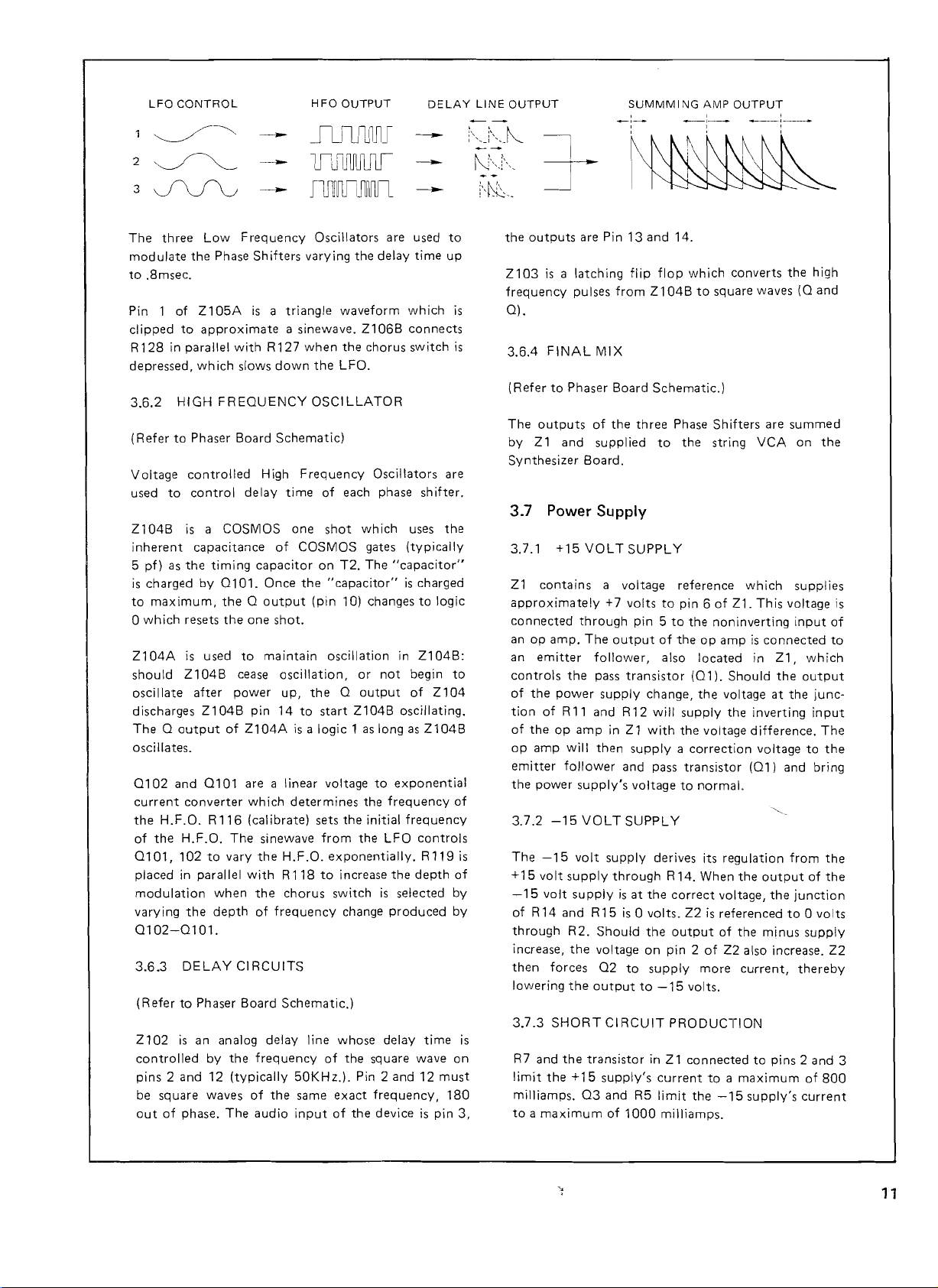
LFO
CONTROL
HFO
OUTPUT
-llUlJlJ1JIJ
DELAY
LINE
OUTPUT
SUMMMING
AMP
OUTPUT
The
three
Low
modulate
to
Pin 1 of Z 1
clipped
R
128
depressed,
3.6.2
(Refer
Voltage
used
Z1
inherent
5 pf) as
is
to
o
Z104A
should
oscillate
discharges Z104B
The 0 output
oscillates.
0102
current
the
of
0101,102
placed
modulation
varying
0102-0101.
3.6.3
(Refer
Z102
controlled
pins 2 and
be
out
the
.8msec.
to
approximate a sinewave.
in parallel
which
HIGH
to
Phaser
controlled
to
control
04B
is
capacitance
the
charged
maximum,
wh
the
by
ich resets
is
Z104B
after
and
converter
H.F.O. R116
H.F.O.
in
parallel
the
DELAY
to
Phaser
is
an
square
of
phase.
Phase
05A
FREOUENCY
a COSMOS
timing
0101.
the 0 output
the
used
0101
to
when
depth
analog
by
12
waves
uJlJlJIJUlJ
ru1lnnJf~rl
Frequency
Shifters
is a triangle
with R127
slows
Board
High
delay
capacitor
Once
one
to
maintain
cease
power
pin
of
Z104A
are a Iinear voltage
which
(calibrate)
The
sinewave
vary
the
with
the
of
CIRCUITS
Board
delay
the
frequency
(typically
of
The
audio
Oscillators
varying
when
down
the
OSCILLATOR
Schematic)
Frequency
time
one
of
COSMOS
the
(pin 10)
shot.
oscillation,
up,
the 0 output
14
to
is
a logic 1 as long as
determines
sets
H.F.O.
R118
chorus
frequency
Schematic.)
line
50KHz.).
the
same
input
the
delay
waveform
Z106B
the
chorus
LFO.
Oscillators
of
each phase
shot
wh
ich uses
gates
on
T2.
The
"capacitor"
changes
oscillation
or
not
start
Z104B
to
the
the
initial
from
the
LFO
exponentially.
to
increase
switch
of
of
change
whose
the
Pin 2
exact
the
is
delay
square
frequency,
device
--
are used
time
wh
ich
connects
switch
shifter.
(typically
"capacitor"
is
charged
to
logic
in
Z104B:
begin
of
Z104
oscillating.
Z104B
exponential
frequency
frequency
controls
R119
the
depth
selected
produced
time
wave
and
12
is
pin
to
up
is
is
are
the
to
of
of
by
by
on
must
180
3,
is
is
the
outputs
Z103
is a latching
frequency
0).
3.6.4
(Refer
The
by
Synthesizer
3.7
3.7.1
Z1
approximately
connected
an
an
controls
of
tion
of
op
emitter
the
3.7.2
The
+15
-15
of
through
increase,
then
lowering
3.7.3
R7
limit
milliamps.
to a maximum
pulses
FINAL
to
Phaser
outputs
Z1
and
Power Supply
+15VOLTSUPPLY
contains
op
amp.
emitter
the
the
power
of R11
the
op
amp
will
follower
power
-15
-15
volt
supply
volt
supply
R14
and
R2.
the
forces
the
SHORT
and
the
the
+15
are Pin
MIX
of
the
supplied
Board.
a voltage
+7
through
The
follower,
pass
supply
and R12
amp
in Z1
then
supply's
VOLT
volt
supply
R15
Should
voltage
02
output
CIRCUIT
transistor
supply's
03
and
of
13
and
14.
flip
flop
which
from
Z104B
Board
three
volts
pin 5
output
transistor
change,
with
supply a correction
and
voltage
SUPPLY
through
is
at
the
is 0 volts.
the
on
to
supply
to
in Z1
R5
1000
to
Schematic.)
Phase
to
the
reference
to
pin 6
to
the
of
the
op
also
located
(01).
the
will
supply
the
voltage
pass
transistor
to
normal.
derives its
R14.
When
correct
Z2
is
output
pin 2
of
more
-15
volts.
PRODUCTION
connected
current
limit
the
milliamps.
converts
square
Shifters
string
of
Z1.
noninverting
amp
Should
voltage
the
regulation
the
voltage,
referenced
of
the
Z2 also increase.
current,
to a maximum
-15
the
waves
are
VCA
which
Th
is
voltage
is
connected
in
Z1,
the
at
inverting
difference.
voltage
(01)
and
output
the
to 0 volts
minus
to
pins 2 and
supply's
high
(0
and
summed
on
the
supplies
input
which
output
the
junc-
input
The
to
the
bring
from
the
of
the
junction
supply
Z2
thereby
of
800
current
is
of
to
3
11
Page 13
SECTION
,r
.
1,1
,
A.
Remove
all
4
ASSEMBLY/DISASSEMBLY
10
screws
as
indicated.
TUNE
CONTROL
B.
to
Lift
clear
rear
Tune
of
instrument
Control).
3-4
inches
(high
enough
C. Pull
forward
SECTION 5
5.1
LM339 Comparator
The
LM339
voltage
the
comparators.
LM339
OUTPUT
2-3
contains
is
OUTPUT
3 GJ\ID
14
inches.
GENERAL
four
With
compatible
4
INPUT
12
INPUT
INFORMATION
independent
an
open
collector
with
TTL
4+
,-
precIsion
output.
and CMOS.
D.
Lift
In
the
-15V.
(voltage
chassis
OMN I, pin
Thus
the
determined
straight
12
ouput
by
up.
of
LM
states
external
V+
339s
of
are
connected
the
device
circuitry)
~
are
or
..
to
open
·15V.
08
12
Page 14

SECTION
6
CALIBRATIOI\lS
6.1 Synthesizer Board
REF.
R22
TRIMMER
VCF
CVR
0
R16
VCF
CAL
0
Synthesizer Control Board
6.2
R14
SYNTH
VCA
CVR
0
Trim
Procedure
Monitor
1.
Put the
2.
Put the
3.
Set the
4.
DOWN,
Adjust
5.
Monitor
1.
2.
CI
Put the
3.
UP;
Adjust
4.
Trim
Procedure
Monitor
1.
Set all
2.
Put the
3.
4. Put the
5.
Set
DOWN,
Put all
6.
7.
Adjust
depressing keys.
pin 10
VCF
VCF
ADSR
RELEASE
R22
pin 10
ip a 33K
VCF
put
all
R16
the
VOICE
MIX
MASTER
ADSR
RELEASE
other
R14
of
filter
FREQ
"ADSR"
sliders
for
minimum
of
filter
ohm
resistor
FREQ
other
sliders DOWN.
for a 16Hz
high level
SELECTION
slider
fully
VOLUME
sliders
as
sliders at
for
minimum
TRIM
module
slider and
slider
as
follows:
DOWN.
amplitude
module
from
slider
fully
sinewave.
output
LEFT
follows:
DOWN.
minimum.
deflection
PROCEDURE
Ml
with
VCF
RESONANCE
fully
UP.
ATTACK
when
Ml
with
pin 10
of
DOWN and the
of
the
Omni
switches
fully
OFF
(synthesizer).
RIGHT
ATTACK
of
an
oscilloscope.
slider
DOWN,
keys are depressed.
an
oscilloscope.
M 1
to
with
(out).
(maximum).
DOWN,
the
oscilloscope trace
DECAY
pin 2.
VCF
an
oscilloscope.
DECAY
RESONANCE
fully
3/4
DOWN.
3/4
UP,
while
UP,
SUSTAIN
slider
SUSTAIN
repeatedly
fully
R33
0
.
6.3
Phaser Board
R
116
0
R216
0
R316
0
6.4
Power supply
R19
0
STRING
VCA
HFO
HFO
HFO
+15
VOLT
CVR
Trim
CAL
CAL
CAL
Trim
2.
3.
4.
Procedure
1
2.
3.
2 1.
2.
3.
3
2.
Procedure
SET
Perform
1.
Move
Depress
Adjust
depressing keys in the highest octave.
Monitor
1.
Attach a lOOK
Adjust R116
Monitor
Attach a lOOK
Adjust
Monitor
1.
Attach a lOOK
3.
Adjust
1.
Monitor
2.
Adjust
the
R33
R216
R316
R19
the
MIX
(turn
for
TP7
TP9
TPll
the
synth.
VCA
CVR
slider
to
fully
on) the
(Z102)
for
with a frequency
for a 20.4
for a 11.3
power supply's
for
STRING
minimum
ohm
an
ohm
with a frequency
ohm
exactly
deflection
with a frequency
resistor
11
microsecond period square wave (+O.l-{}1icroseconds).
resistor
microsecond period squarewave (+0.1
resistor
microsecond period squarewave (+0.1
+15.00
trim
procedure.
RIGHT
from
from
from
+15
(string).
BASS voice selection switch
of
the
oscilloscope trace
counter.
+15V
supply
to
TP6.
counter.
the
+15V
supply
to
counter.
the
+15V
supply
to
volt
output
volts.
with a digital
TP8.
TP10.
(only).
while
repeatedly
microseconds).
microseconds).
voltmeter.
R20
0
-15
VOLT
SET
1.
2.
3.
Set R5
Put
the
and
put
Adjust
(+15
volts)
first.
digital
voltmeter's
the
meter's plus lead on
R20
for
exactly
ground lead on the
the
power
+15.00
volts
(reversed
power
supply's
polarity).
supply's ·15
ground
output.
volt
output
13
Page 15

....
.Po
'5)'NTh'E~j7CRW
oVr"pur
1\
''''
"'n
,<.".'
~~
•-.• v -
uvn~
.....
"
7520fjnl
E I
~
---D
"
~
-
m
~
~
~-
"
I
Ph'A5£RBO.
72//80/
~
~~~
QjL
."
K
5PE£P(,O,v~~~[
MOlJiJi. A
Mt9PU'ATO.lr'(JUrI'VT
-
1
P/4-
__
~::.J.:_
-/H
fOR
-~7J..--·---'.t11
/:;~~ !,~/~~.,
_._ .._-
£.(f
Gt~
..
"
---",f
•.
_-,._-~.
---
,
I
I
I
I
I
I
I
I
I
I
I
/"IUE,('
(<JAlTRtll..
",-
..
"
,~~.,,"
......
SYNT;;FY",
STRING
CONTROLBD
7212201
6ATE
C/ur
=rr1
r~
••••
ZER{'I'YVTROL
72'<3
T!?/6"Vf'
=-]
1l1ill
".
BO'
L
OWER
VOICING
~,
......
.~"
~~~
~
...
-,
fi(;::::
:"!,,,,,",,,,.
__
-,'5rk',v&
--
~ft
~~tr'
~:;~",,"'<rTR£"C<
..
-
'n
__
==-C;';""
j
~--
~~c:;
_~~~
-=-_-=C,,:::,
m
~_
~_
.----,.~."
...
==-~.==~~~:
~_._p,o~
. ~ .
7211901
_,
..
.
WI~£
,~JW='·I·"M~·IIIIII
BO.
'
I""'"
fER
5if'I'Lr
7SI9<;;01
f/~y'Ourl',r
'/SVS~N!,C
-.-=----~~~'!~~_~
JI7
1
.t,
.to
J7
f'2
"":SEAlSil
~~f:[ff!:r
-:3J
J-J-..
"-->-....
~
c
Til
1/5VtJ,A!L
T3
Y
7212001
,I''''
"
~
L
~-
J-
1
_L.~,
O
NNECT/ON
~~
SWITCH
S["MKO
C I
:
II L
I
I
I
I
I
I
INTERCONNECTION
OMNI
MODEL
'.~
2480
DIAGRAM
Page 16

I~~
I
II
_
'"
I
--=-=
",W~"""b''':
.'
, M -
"f
'
~H2;--
R16
'_-
I----=--=--=---=-~=~:=--
I
,"
----- -
---
---
__ -_
"-,;ci,~,,ji;";'C6ii'rn~;:-':~~'"7-~---'=-6=-==-===-
----
en en
-~'"O;i;;;:C'-~~_-~F
----'-==~\
m""
l
.c----
'0
J
__
-.-------=:::..:
_"
_r I \
r-
l}J'i''10e>
"-
r-
II
, I /
I
, / /
,/'/
/
PC
bel
H
316
"KEYBOARD"
/-------//
/~--
---;:::.~--
---I
)
I,
J2
Ii
;i 6
/j
r
l'~X'--
//
/~
/'
/
/;</
tf
\;1
I:;
t: \ __
\:
J3
11\
.-J~LJ!r~_
//
H
19
""",'
(t15V)
'\ \ J4
\:t,\~\,6::,
__
.....
U1
~~------------=--------
DESCRIPTION
FINAL
ASSY
240V
SEMKO
FINAL
ASSY
'20V
CSA,
LA
FINAL
240V
ASSY
STANDARD
------
BRN
TO
POWER
SWITCH,
BLK
SUPPL
BRN
SUPPLY,
TO
Y,
TO
PIN
5
POWER
E-'
POWER
E-'
LINE
CORD
BLU
TO
SWITCH,
WHTTO
SUPPL
BLU
TO
SUPPLY,
CONNECTIONS
POWER
PIN
6
POWER
Y,
E-2
POWER
E-4
GRN/YEL
GRN
GRN/YEL
TO
TO
GND
TO
GND
GND
SCREW
SCREW
SCREW
PIN 2
TO
POWE R SUP E-3
BLK
TO
POWER
SUPPL
Y,
BLK
TO
POWER
SUPPLY,
POWER
E-'
E-'
CORD
PIN'
TO
POWER
RED
TO
SUPPLY,
RED
TO
SUPPLY,
CONNECTIONS
SUP E-4
POWER
E-2
POWER
E-2
WHTTOPOWER
SUPPLY,
WHTTOPOWER
SUPPLY,E~
NONE
E~
Page 17

C'l
NOlE,:
~OI_D
1I~l:.
")
ARt.
flue
,"
MASTER
(UPPER
OSC~ATOR
VOICING
u
rOPO<,TAVC
DIVJLJER
~RYO,t'.."'I,u(j.B/).)
(J
"l
,c;/~~%;;:~Y
(UPPEU~/""'80)1
~OOT
JWlrt:,u
)'LOWEK
r--
IJk o'l"-!"y-"w,.'1rc'/IES
r~r
UPPr;R
&15
I!P~~R
_T--
-
I
BD)
l..rtf
!,WE5
e;,hJTOC7
JU
TONE5
CZ
,.
To63
I "
-l
2=-1_,'-"--'--_+-+__..
, I
..
~~~::Ero:~;-'
CONV,,-""TEs;'
((/pr~~
¥~
<:1#6
/.
(LOWE~
YtJ/~fNi58D)
!
A
.•
_
eJj:/t~Ie~"P':J;~
~w'r<,J
'SWVllo'('(wrep<
..
_'<;(/5
TAl"!
OVO<<'''''.
;'OI('f-"'6BOJ
+
.5d,PPNE5stOA/
TA/tu;e.t<!
6I1NEN/lrO~
1.0W<!",e WK/;\'(SB.t>
~
O~R
J,;V~/Al'GB1>J
r J
TI)A-E561t{7
8/!
I
~
TONt'"~
TO;""
1'{'_Ta.¥E5
8ci
~t/5rAIN
:J1/$rAII'/Rrr.
.!'~.0f~r
+
~--
~
-------+-
I
G"3
TOC"
<3
TOO'
I
1'063
~ -----~-----.
t:2
~
$(/5
1-----1----1
-'
-----+--------\
I
H.
TONES
G"'4TuC714''jAr~
~E!!...W/,!/{~_E'j-~9
r>~.
TONe'!,
C 3
TO
K£r.'fw/TC#€:J
~.
/.20
------~
(.//'-':'-//T
•
WP,PfR
vU'l(p./6FlJ)
,~-4'
OjVE{!
Vc?/(I#r~
~~:'"_~~~-~
...
11'.-;,4
~-,
~f...
-(.'~:/{".'
nrrw",'NIJI'"
"~-iONO(i'
A1""'~"""/<'N'E;l/-rl?
Jf',IJ
co:.
.'
T.
I
IOPPO
YOI<,w68D)
63
~OWI:'RrOIt'..w6trl>.)
,I
--
-r~Y:E~;~~t=-:rr
--:T,f'/A,.'(;Ra€.o1~",
CONrROL_
(5nf'IN<$('O,(/r"",:u.lJ~
BA5E.CAre
VT&NI~
A'EYIN{j
('.?TP6~
~
('I!?<.·~II
/,,-"WAhtJrr4'Id't/n-)
lJ8
f
RA5.5
(j
I--
"NTH
Bt>}
r
.Ali?
('~TROl
i
A
"
6,4rE
HlJ"
/i,4f5
VOLtt,H~~
:S(NTJI{'dV7Prl'
5iRIIVG
, t •
14
/
5£t€t!r
V(!ICF.
...-++'
, I ,..I
I 1 I
-~.-:
~'
SA"
I'
1/~'8A<S
/5TI1/""'6
J'f'YA/'~I'VE5/~~R
'5~l~c'no'"
.'I'
,.f'/?/J<,:,\
~/1O'8,tlS".5
15'(Nrll,
~~~~~t
..sPEED
(~dNT#
I
Ct!NT
V~/C"
(!NvT.
Bo,)
80)
LFO
l'cJ"-'TR(!t BIJ)
f+
(}}'VT,(tlL
t
4C':5R
t
GAT/N6
/_'rNTkc5IZER
BI»
I---+--l--.--
Sb)r
~
__
_0
----------
«r,vrPE'fI?EP
H
vcr
I I
~
y
v
~~~:J
) -
L-
po)
~
5TRIA/u
Ve,of
(.~
y'NT/>
(',:!NT:
liP.)
---,----
L_4-
V,
...
A
f:5fillTl-,(1?NrmLSb)I
1
~
.
··It;YNT
l
GAr,;
(<;
Pf?(J(~5SIN(j
....
£SI.!''
....
SO)
OuTPPTM/)
OJrN
"'LJvr
:5YIIOfE"5IiFCR
8,~"i
1
c(JI,'tlr
-
,,()r?{)T
....
T/A/AL
TKI.
OOT
ooT
,~
y
/
PU'~~
(LOWER
OJfIVA"
MJ.:'W69fJ)
~~~
OMNI
MODEL
BLOCK
2480
DIAGRAM
Page 18

'/5V:::/:~
05
.9 <'-
__
-+----,
:~7:
-/.5\1
if:I
;C>~
,>V
CI
'~~'''.
~9,"o
..
n.
-->-
,.
",
12.'!!.'4,/~,,~
~ = :c~~::R.;-:
/~C'6l _ ""'ON~
./
~/
-
r""o
...
o/i,-r~::u2Ip~c.u
c"rb
P,-",c&:s
",,,,.£,ARIN/i
~
h
I •
~rti.~'
I.
v"''-£s~
o,..
../t./111_,3/t.
"'/t.~'lro'"
2,~~~~;O;'
...
2..
~':l"O."".e,').'
z:
L 3
2.
....
i!~,
,
J
"'''''''£50'''
"tE.F"
....
'ON~t:.Nr'ONS
....
OLTAGO£
t
TJMp~
~A
..
",lt.t.
"".t'-,':..~~,,~,/111/t.
...
/~J6
01:~,
01:1'.
2"
PC'I.'
Vt.£t!
CONNt:,C'r/ON!'o
INP,-I£~
~"ccln/t.o·
"'/11111:
IN "'....
..."
IN
A$
ARE. CP..
Altlt.
"2.1",'
C"'S,C.q1''2"£2,L.I,P,,.,
QI,
A19,
Z,"]
~OR
SuP""-",
'
.,~""
T
("'.,."O'--
Of>~B£
....
/III,t,D.)
P6-)
.IJJ-.. .IJJ-..
P"-I
P"-16
~'-
P1-1!
.IJJ-..
P6
.IJJ-..
_rUL
P6
-13
P6
MJ...
-II
MJ...
-2,
P6
.IJJ-..
-8
P'6
.lJJ-..
-6
S'cS'L
PS-;2
82
P6-4
.IJJ-.. MJ... .IJJ-..
SUl..
P&
·5
P7-IJ
..----W:.
OMNI MODEL 2480
PC
SCHEMATIC
BOARD, "UPPER
1
of
2
I
VOICING"
17
Page 19

V2"~
~II<J
I~o><
4'0
GAT£
'Z.lIt>"
/SOK
~.,
150K
I",
.'
C
,-----'>pn-2
~----@j
1.
I
,I
,
~
;)17-
.'
C
3
~/~o<
MS
~'4
/001«
R,.
1001<
",,'-
IOO#<,
11'
3s,""
I~OI(
,
t::::J
--<'~
I~
KVW
,~
~
.
~
c'C'i'
Dtill
18
GAT€
4'A
GA.TE
!
I.-
'i
4'.
OMNI
MODEL
PC
BOARD,
SCHEMATIC
"UPPER
2
of
2
2480
VOICING"
c
Page 20

Page 21
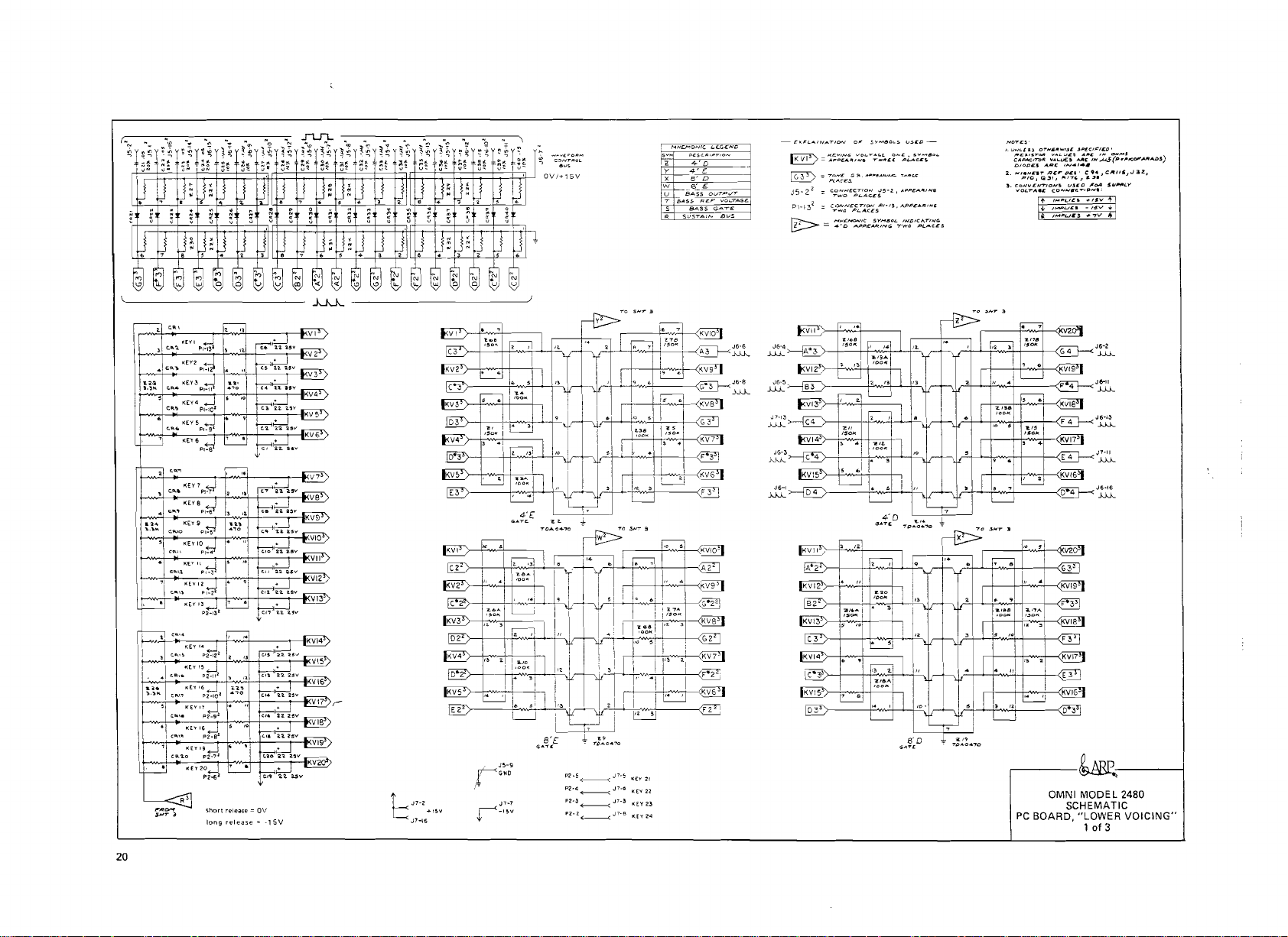
r..
"\0
N - - - - -
"", ..",
.......
"0
......
~
cO
1~I~~rl~r~~rl~r~~I~;rl~Il~rl~I'~I'
5;
T~~
T~~ T~; T~;
...........
T8;
T5~ T~'
Te,
'"
d;
"","",
T5;
T5
"_
I'~I
d'T
"",.>iE·O/V"
&U,
OV/+15V
MN~ONIC
~~MI
I-f..G£Nl)
;:
i
~ = :;::~
~
~/
J5-
PI-13~
~
~
...
6",V.;'~<''''-~:'~,(~'''~':':;c~l!I''''
;:
ToNE
G
~,""."e,l.k/AIC.
....
T~C;;SP'.I',
SYNlJOL
T","'U;
,l.PPEA"''''~
...
PPE
IH/:lIC"'TIHCO
TWO
PUIC£,.5..
2 2
;:
c.~::;;E:~::'~~E~5~2.,
= c
.....
O::::€}
N;.I£~/C
=
"'D
APP€_//V~
....
R'''''
PLACES
""OTC:~
I.
I.J'-I"£
&~
OT,.,~,JfIN/J£
.....
c:,s'ST_
""'''I.JL~
~~~~~~;;~~~.7:~
2
....
,.",CIT
RC~
PfC,
Ciil;"1
\fOL~"'.C
""7~,,,,jI'
Cl;>""""~C""/~"""
t I....
·LIE
'" , __
~
,,,,,,pu
,.
r::OHVe.N7"ION"
JPE.C/~/Cl)'
....~ '''' "'......
PLI'
v.J~/:l
10
LJ~
~
,
..
IN
e '''',
~cA
",'$V
"",7V
AJ(p"
CIIf/iS,J
SU_LY
•
J
.cC#'_
...
D5)
:il2,
shOrl release = QV
long
release
c,'·'""
-,5V
0:
J6-6
J6-4
JJJ... JJJ...
JJJ...
J6-8
JJJ...
'0
"
~
J6~Z
J6-11
JJJ...
J6·1~
JJ.J.-
P'II
.uJ-
J6-16
JJJ...
• "A?l
t
J!>-!il
UV
'H
---<
....
b
J7-\5
yGND
/*
r-I!>V
J7~7
I!>V
P2-5
-<-------------
J7-5
P2'4~J7-GI<EY22
P2'~~J7'~
P2-2~J7-B
I<ty
I<Eva
21
~
r---~,.-,
OMNI
MODEL
BOARD,
SCHEMATIC
"LOWER
,
PC
of
2480
VOICING"
3
-----1
20
Page 22

(
1
J5·11
C2
==,,-""-.l.-r---,--'-"'-L.!-------O,,'--'---~
Ye',
f------J
J6-I0
:
1
c::~"..
Yo,
J6~IZI
"V"\f
J~!-I~!
I
C""'02.5AC
0"
Y"
:
I
'D~::'~ I CD::"~,':l;
~C'::::';f
I :
I
ov
~
...
.
.
.
.
~ ~
I I I
J~·t31
~
c~;;.~
J5-~1 J5-4~
F'
iF"
Cl't
..
& r
J~'J,l
]'''
I
J~·81
--'"lJ"L
J5-IZ
82
~,q52
I
1
J5-I0
1"
:::""'$~
J6-9!
,,',
J6.14
0'
c.
1~:O:r',H;
\
1
...
~s
J5-1
1
T
v·I
PI-I"
KEYI
4
~,.",
I<EYZ
~
E""
KEY
EXAMPLE:
key
down
P1
•
",i
(D1
depreBed)
,
3
=
-1
5V
l:I-I0'
KEY4
b,·,·
KEY5
I,,··'
KEY6
L;.
".,'
KE'l1
--0>
PH'
I".,' I ,,·z' Iez-,,'
K(\"IO
1':011
'-->
~~
iL4'
,4t,
IKOl2
'-->
,47
4
;l,3'!l,3
I«YI3
~
....
37,
~I!l,
.lS,106,
3'1
z
f
..
a,,,,,
...
z,
...
~,4-+
".,'
K[Tt9
key
up/key
down
, I
PC
~<
OMNI
MODEL
SCHEMATIC
BOARD, "LOWER
2
of
3
2480
VOICING"
21
Page 23

N
N
synth
8',
16'
\
JII-9
>---.---+---1
r
~o~
on = +15V
off
= OV "
y'
",'
""
'H
<D<~'"
BASS
DISABLE
4'
S
POLY
".
'::,16
.",
Ih
~1
I~O
·"·
-
QI'
!U3'O'
•
~o~
~!.
__--->
--
i:~
la~
-14.5V/-13.8V
PI/"J
"V
·15V
\:,,~"
.-
"'
,-
,-;;q
.... 8 ..
1
.,
~:.'
-
<i---
PI·/
vp,;c"l
",tc..-t/.,,,"'IJ
Ov,
c.
...
,f!
,jJl-
/OV
7
>---11---
A,
••
101'
~
.....
@2V
pop
---<
,)/1-/6
---1:"2:::
""''I'"
H
FfDETECTOR
.
l~_.
I
7~"
IJlI
A U
_._~
';:.
"i?"
UPPER
BUS
TRIGGER
UPPER
GATE
.,
••
DETECTOR
, "
BUS
.,-
___ ~ _________
".
,.".
~.o
c
,,<A
t+
...
~.\10[
,
..
1
15V
.~
d"
l",'''04o
~I:J.
,.~
__
l-2_
~::'
[F~-9.'-'
CIt"<J
~
7:;"'-
~t(
1
SUSTAiN
PULSE
~:~
J!.
CD4"""""
DRIvE
l:t+-
$1.
_O_V_E_R...:R",:ID;:E=--J"~
_____
~:~-y
~
*~:
~
:t;:',
I
~5V
11
J:
l.i
t-&>'
-<';"'-Jf
OV
'JL
JL..·
I
'
~v;~~
:
L-"JI"'/lT;H
J
,,;f3:;;;::n
PIO'Z
..t:,.""""c~
,V,rA,.
';;~~.
J'-I
JJI-/I
_.-.
15V
.-------r---t----------t--~
.,
..
oJ17-5
.'".,
J"-4
,_.
r_~
>-~_"_:_3_'_"_--+_++
~'S::---+-Hf-----""t--'----t---
r
....
,::
,
~
..
~
~
,,,,e,_,,
ul :
J1Jl!
tone
,)
/1-
3
.'
...
",r",
.)" -14
1It'",>'",_
,)11-8
,~;;'":
WAVE9HAPING
I ,
8'
e'
SUM
I~
""11
BASS
c;""os
,.,~
I
1
,""
11
.M.
'C"'(J~
-t_-+ .
':':
1(1" 1"" 2..,.
~:W~:"
'D'"
All'
,-
"1"
JI.....
~
'--J
-:":'
-:::"
1~';':(l
lAn
--1---._-
~
c--_. ..
----
.--
'':~
'.:~. ~ ,~:':''':'_.
r....
I:~s'o"
~'"
.'1<
.71';
""1'\
,.,_
.,./0(
+ 2...
1
BASS
':",--:;i~
10
..
.
:
-;=-
'C"'04o
~
_
-r-Lf""1..-
down
• so..
t*---
I
of
"'''~
:1,1<
\.....r
...
'M
-':".::'-::=r:,:rr;~~:~"I-·--·--_[~t_:~~'~';N
-------"JI,IO,•.-
.~
...
'o~
-----~-]
,,,","
fl8~
i
10M.
- J
f·-'-:-
•.
'00..
.,
-0TT;;--'::~-
l
..
""
'20]1.
1
8:1"
~
~I/.
Y'"
r---
C""
20)11
...,
IW~
11<1,
~
..
::
-
~.::.,
I !
,.'1.
1.-. 16
. I
(;f~==-::"~-~l
IL
_~
;L
~f.F
l'H
-r-
'CD-+O'~"£
WAVESHAPING
key
up/key
vt.v1-v1
2V
p.p
.111-
----<
10
<CJ-
0I7/~15V I ~;:.J-~f!~
~>-.-
_~_
C
I'''''''
/NHI'
2
R[FERANCE
r-~==-===;-]
,~~~~
<00
,'.:~~
AI~'"
- .
-*--c-
...
~----...-
_f
,q
173
4,.IIK
."
~H
J90"
~L--~
.,::K
2
~..
471';
2.N,.".
AI.'
J
-:::.
KEnNG
GENERATOR
.1
A,~H
-r::-
I:::::
,,2.
,".:,.
-.
1"
,..
~'"
CONTAOL
~'·~;r1
BASS
"II....
'o~
WAVEFORM
~'"
( c
~'::-r;;l
"
100'<
..
~
"I,'::
'R---:;;;:;;"~"
I
~I
;1.7'"
..
.,."
CI"Jo'l:
l1li'7.
,,.
,
"f
_T
LOWER
BUS
GATE
DETECTO~
~~:~L----
(.::::~
~
I:"
.~~
l
1IIt-I!J~
oI-l!JV
JIH,
GND
PIO-I
-~/'<I:JC
P.-'
,)11-14
-t,V
ull-~
I.'
I... -~/
~~f;~:'.
I
PC
==t
0(
_
=1
JlY"IIN.
OMNI
BOARD,
OV/+15V
0
11
T'\
~-----,
MODEL
SCHEMATIC
"LOWER
3
of
3
~:::
,,'
...
".
l1li1.'
,.~
__
_.
,.
. T
C8'
.sv
I
r-
~~..
.
".
~
T'\
.~
2480
VOICING"
-:.
.J~-1"
'o,,~~~'::;-
~
r:?~·v6
.....
po"
..
,_/'V,.
:P'_4
~~:~:
P8-/
·I§
..
,~.,
Page 24

Page 25
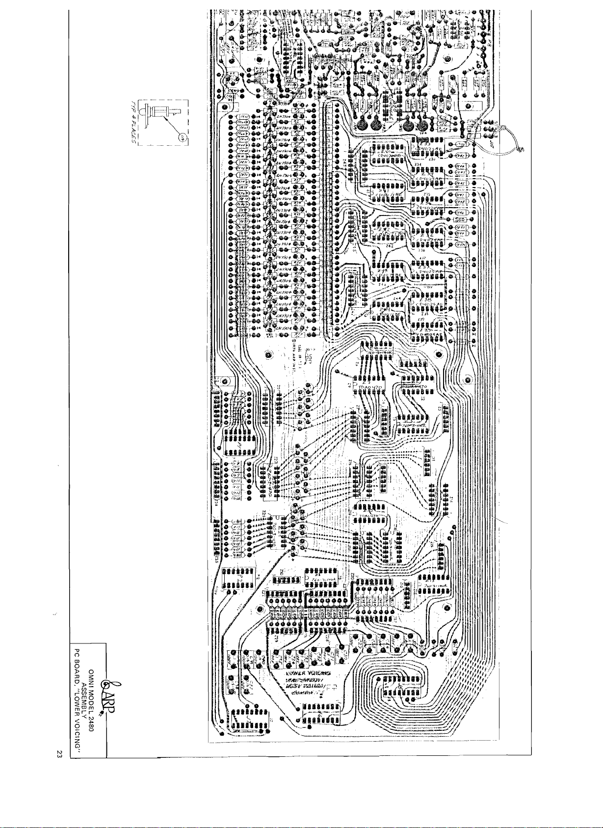
N
w
"tJ
n
co
o
:l>
~~~
~~g
m"'m
:o~r
(§
- 0
Q
z
GJ
l.--_-----'-
0
t
i
,1'
I
I
I
I I
I
--~----------
~
~
-
-~_
..
_--- _
...
--
--_
..
__
..
_-_.
___.J
Page 26

N
~
!l'OollH
TO
'VNTH
MOO'
fNA.ltLC
~s
GAr£
TO
.7V
~
~~J~--=<4~~
BASS
a"-:;-
JI3-H>-~--i
J/:lHi)--
JU-l
~
/1
JI3-7)
(
.IUf
I'"
~liv
R<
-
I.l.
-13V
-
/QV
-""-
,
(
/
CAl
"
'.21<
T j
------r:E---
'~4?!i
f+---+--
-=-
(fIe
RlI
Hl4148
'"''
I
.~,~',
'" r -
rn~148
lN4'4!!
2N3He
CAIO~'
1<1
~~~
ADSR
BLANK
ING
'"
""
STR
ING
VOiCE
_~~
2 r
••
&
Iiu
_
=
SELECTION
~JI
..J
SR4f
>2.~
{
U
-12V
not
OV
selee
'"
"'Ll j
ted
~
+1OV
-1
R2I
""
I
_~<
.-+--+
t-.---t-t
t--t _
,~
~
CI4
''''
",
'"''
AR
l.--
JU-9
'"
,"'"
AOSR
ADSIt
OV/-15V
'-
9
}40
n~
R£lUS£
IllAHKING
AR
SQUELCH
HC
C-<>'O£
OV/-15V
,.t
"
''''
£
H
CAli
11'141411
"+
J
"-
j------<JU--<l
AR
SUPPRESSION
"',
~
>-t'.!.'
-r-+---',M---1~I--~a-~
C..,339£
H,
'"
OV/-15V
'"~
1.'''
COHTROC.
I«JT£S:
, LN...£SS OTHER'IlIS'E
R(SISTOR VAll.{S
CAPA,CIrOR
(P
..
CRI.2.
2. HIGlI(ST
J'21
,PI.,QJ.R41'L~u,l4
,
COHV£lH
YIJl
rAGE
VAl~'
PicorARADS,
S. 4 ARE
REF
DES;
rON'
USEe
CIJI'foI(CTIOHS:
~[CIF'[O:
.tJl(
u~
67,47':Z
Clll.CRI.3.
FOR
'"
11'1
.'lLf'9ly
CUIS
IH
In
"'"
,_
~.
(-
\,
{lOng
short
P"-'~l
release =
release =
STR
~ELEASE
-15V
+8V
ING
de
de
~
, I
,2.',
rowAROS
~
TrIl'NTHAU
i ,
OMNI
MODEL
2480
SCHEMATIC
PC
BOARD,
"STRING
CONTROL"
I
rdJ
R31,311
llASE
VIEWS
lOOK11olG
,
1
~::
1
Tv
Ill'
IIV
/
Page 27

l!)
N
Page 28

N
en
.'
a'
Ill'
I"«.y
PQT
8'
!>TN"Hllln~
ST1i1'l'l 6ASS
'(Ole(
vo,C'(
PIl
{
"'-'11
I'11-lf·
{
1'1'-2
1'11-3
I'll-IS
••
,lf-
E--
-
---'Ul-
~
t-t
~IHJ
~
...
i
11!l~
l__
1'12-15
"H'gI
{
'is'
'''-is
':;':;a~--
1'12-13
".,
{
;;:;~:Bi'
1'12--
_16'1
1'1'-4
{
JI4-J
+7'1
1'12-'
"HS
{
PI
~-l
b'
il.
it "
MAS(
AD.'lR
AD5A 1ll.\Io'KINGl
ll'
STillING
III'
STR''''
I«lO 'HrUT
~-~
~.---
GAT£
1'12-7
f----
"HS
{
1'15-7
'"-"--'
QRlv£{P12-11
f--------J
RnhSE
"'-.~
{
1'1
J~lJ
"'-.--.
L.-~
{
PJJ-lI~
IUS
"H'p
{
PIJ-J
"
....
~
lASS
PI'-14~
{
JIH'~
{
PIJ-fI
P
11-12
f---------r---l
{
'NO
JI4'-1~
-;;
III
~
t
-15V/-13V
8l~
A12,2'.44.1'I1
!lASE
vTr
....
S l(l(J(IHCl
TOWA~5
~~
~
51.1.'.
Tf~INAlS
+,6,8
0.1
2N:'IIJ'.
...
-"v\I\r
"
1cl2
'f'"
~,sv
/
PC
BOARD,
lfO
~OV
-15V
I'll-I
liAS 5 .tA
OMNI
NOT[S:
TD
vcr
2.
~~
MODEL
SCHEMATIC
"SYNTHESIZER
2480
.J
CONTROL"
Page 29

u
j
Page 30

Page 31

.,'
I\J
00
III'
I
-JA~I<;
0-;'
~l:fl
In"
[]];:J-"-'-<:~~
~
,
I - I
I
~~i£RNAL
'"""
I CONrllOL 1
, I
L !
+7
.5V
(-2V
T
-/5V
·1V
~
13
V
JL
-15V
r:? I '
y::s
w/footswitch
~,~m,
::~':';~:;~
ADSR~~G':I~~~-l~L
.-.,..PUL5£
/-2V
~GH'
It
"'Ttl
Jl~-l
RS'
>--t--~.t
r
!
..
~
.'eo"m-,,;r-I-~+--W
8'
POLY
J12-2
>--
8'
~ASS
In-3
BASS
J12-14
lFD
J12~
r---I~---;pt
;A~El-
- I
,
I
f=1
JIS-3
:
f~
m-,~
L'16-'
,,\
-l
..J
7
'15V
Jll'15
eRS
I"'''\~¢I
GNO
JI,-ll
>
GNO
JI2-IJ
CR91N4HI
-'"
",..
)-.---
I~===
held)
-i-
OR[Y(
JI],-II
r-'
J''''~,
I----'I:l~
'I
R62
I()~K
'
LI
•
[LJ
R7
'
LIN
"
f
~
1--'
~1~
RI'!
68,1,'
~
~
1'-I4tH
'27
471'11<
GATE
PROCESSING
-~
CO'¢J<AE
LFO
OUTPUT
4
~~
============
I2=~
-'i't--r---w~T
JRiK
__
"
'"
----1
f-----
'"
'"'_].
lJ
---I"RI4
lililK
LIN
".
~+
lHI4S8N
,I±
,----------.
(II
'"
JlK
J
~~~~---
AOSR
l------'YV'~I
~~1'
C7
.1JU
r2:~
PEO,l..l
II
ACe.
GAT
C~~22
21!1'"
'"
'"
'"
JNG
IReSl"
RiEl
""
\1l1I1(
'"
'56
li'll!ll<
VOLTAGE
FILTER
,~~~
'lOR
le~~
J
CII
"EO
~AL'I
'V
.------1
lileK
'"
===I
I
L)
_
1
CONTROLLED
mJ-'J!
,16
l~'~
@
vcr
fREQ
(lieF)
-.-~
fig,
I
1
-.;-
__
R21!1"
l~'~
ADSR
~.!
<R?I
JtJ~~~1(
'
-:-
-~--.-.
r--~--'
_~
--"
2
1
l
_
------~--
e
J,'Z"\,j
~~~
~~-l
~
I<
vcr
1
"m"e
SIlI
R23
391<
-~-~
I
---"
~-L
--~---
7
J'"
--!
6
'de-
cw
@
•211
3
~-
.~~f
31i~
ci0~
J5~
,---r-----r-1
I".
~~JElIl6
:f~'''-W
-----1
-
,'I~
7~::'~"[
--
-*-
3
[l~~"b
~J
L~-~"
[~::~llA'
_
CR2
IN4i4~
-=-
'
.
~-~
5~.
.
'"
f
....
ell
",
6.6K
1/oJ
~
1~6
CR4
1,..4146
II
-
~r!~6KJ
C",.[---
IN34A
[~~
.[
'
--lL
--;---~
l'
t~:~
'-
,uSli:~ " ~'"
R46 4
.'19K
1
f
Q6
2N39il6
-"VV'v--
~~
..
)33K
.i1l!11
'"
20X
J.
7
f=lH
3
I'
~
!l
~
'1':--£,-1.-
L!'13l!1IAN
___
I;I<;Q
33K
R<'~_'
~_
t,}
"
-
J RSJ
,OW,
1'-I414e I RSI 3 .
111
ATUCK
+J~>P
IN414S
I R52 3 -
li"l
--"NY--
."
2::
f&4
~
"OK""
PROCESS
R3l.l
--
TRIGGER
IK
~~491l16
OUTPUT
ING
r
I
1
~I>-------o--rv
m~
: o-J
i.:
-=-
I
PI6-li)I~'V'
I
:
L
-J:C:S
J16~
J16-5
0--1
~N-RE~R-P:'l~-;
['
J35
TlUG
OUT
J34
g
GATE
OUT:
I'
I
I
I
I
I
:
.J
B
il7.14.IEt.2'.24
45.51.5',
6~
BASE
'flfloiS
~
, ,
fHe,ZZ
lOOl(ftjG !OIl.\110 f[Il:I1INALS
.-
I
ADSR
.\/{
Q7 -'3.3
/
.['
''''''
I'"
R58
IH
.loUD
RELEASE
"
S~~:
],
_.---;;"
.loUD
F---'-
AlJ(J
"0;
--~:----~-----<JI2-5
,II
All'
-..a
OUTPUT
/
eRl
loJ
"14~
CJJ
J
-t
.~"''''N
II
A-:>I
'J/
f-
-----<JI:z~llt
~QV
-1QV
NOI[S
I.
UNlESS
Il[S!Shlll
CAPAc/TOO
rp
IUl,;HfST
C16,
J.
(ONY[PoIlIOPol$
VOL
AU~R
ourpUT
orhHhllSE
~
P1CDf,l..R,l..OSl
I1H
CR9.
J35,
UGE
CONNECT
~--"----'~-j
i
ll1f'liES
J-IHPLI~~~
~~
BOARD,
PC
OMNI
MODEL
2480
SCHEMATIC
"SYNTHESIZER"
...
"'LuES
VALUES
DES:
P 16 .Q7
USED
SPECIFIED
ARE
All!:.
~OR
IONS'
"6Y
l"l
IN
,1\61. Z....
5Uf>"L1
r
OHMS
U(
,
,q
Page 32

I
I "
I
I
I
I
I
I
I
I
I
I
I
,~,:<
29
Page 33

w
o
J.lt~
J~ZV:.I".
lltr.
T.
Zll.~
:
~111
ft
..
~~
't,
t~41~~L
>,--------------------~
l1oU'Il1
J
-.
I1:H1
lUI:..
-~~!:
r
~~,".
KJV
r~l'(
,1'.
~
N.LA'L1Nl
R??~
~O:':_-J
LEO
1)(lAY
'''6
!
"t
'::
--
,~l'i
1
r-"'t·
,
';;['.
--"-":)l~'~
,~
,,,
Pl~ ~ '~--
".~
1. ) +
PI'" ll,
QI
,t'~
T<.~
(~l'<.
I~J,'~"
Tt
CI'
1--
·51
(.,
IN
4001
CRL
,.,,1)')1
'"
TP
'L_
!
~;
~
O~LA'1
LFO
-
LFO
LIN\'.3
UM't.'
L
W'(~~:~A
HIG" ERlQ
~
U.J)
no~
O~t'LLA
LINE \
lOR
II\G\I f REI>
m:.l.AY
()~C1ll.MDR
UIoJE
2.
II
--
O'LA'
It;+,~
'rrL!
(l)"lII"-AE.
R'"
''''"
R\\O
nOK
~---
r
..
MK
cb~I"'"
"
-m;-
l')()',(
ij
I
HI""
ER~a
R~l'"
not<
fl
~IB
£.101(
DELA'l
OSCJUATOR
LINE
I
I;;;;:E~L-;:A-=Y~t~IR~t::U::I~1------------ll
3 I
DELAY
lJf:LAY
'
IJHAY
KtA'fL\NEl.
-NLA'
~'RWIT
LINE.
I
T'
.t
C,R(UIT
l-
lI~t
,.
"
L
MQ1U:
L
lJIt,lU\
Q1MU:fla£
~nu'lI[l):
VAlU'~
....
U.",.
lIU1l\
1
I:
1:
'"
.. 1",ru[S
•
.L
(RH
AI'
10
0(\:
W~Ic.ll:'O~,QIO'2..,R.lO,lIO"
eM,
a.U',
GlUt,
tID,
cJ.l.01,Q!m..,
US[t)
F(Ji{
:>lJf'f'\..'1'
'''!'lID
+ISV
-
I~V
'~nJl:!l
+!iV
,yptl{':)
-'!oil
un
Rl.lOj
~
IN
tllb,
~HO.l
.,.
..
Ii:
/JOT
OM",:-tO"'.
jJf.
{we"
Vll.
140LTAbE
USEn)
SI'llll
f'IIII_'-
QU1f'\JT
,)1'"
tl~~
to'l,
r
-,
~
....
19<
RIIO
1.1.1<
10
J:
..
(.\01
~~T
10
L
'!IS'"
""~t
(\~l
+
1.
C.108
10
!~1
..
'"
--
~~,..
,."
••
t
I
j
t--
AU.
All
l
~\c.w\~
lIN[
L1WU:
ULl'E
1
taIoIV~LlllOlJ
rowlJE.c..TION'J'
~
U~)lOIll:
CA"OTO«
~~
I
3
-.----J
~
P14.o;,
',IG.W
INPUT
....
>-------
L
/
.W·
Alll;;.,
i!:\Go,
'leo.
-----4
,.
i~~(.
:+
~~,
OMNI MODEL 2480
SCHEMATIC
PC
BOARD,
"PHASER"
''1
Page 34

31
Page 35

N
W
T'
paWL,,"
/c.XT£.I'''I''l..
Pc.
E\O
~~
CO"D
EXTERNAL
TO
~
POW[
(E:ll'TILRN
pc
SOAP-Oj
q-
~"
F.?_PO~~_
IZOVAG
N[.UTR""'L
CORD
""0
....
fl.O)
GND
~-:-o
NE.VT~""L
NOTE:<;.:
"UNLE.S5
2.
Bt.::I.AFlO
SWITCH
"'L
TO
~
F:=r<
VAC
J7
OTHE~WISE
!ILL
RESISTOR
ALL
CA~ACITOR
(P.
t'ICQF
....
"'LL
0100[.5
HIGHEST
c~ GR.." E
or~R
-M~
~.
f
~~
~~"~
GND,
•
'"
_""tt,,
(EXTERN"L
~_~t~)l,,~:::
Jft'
TO
PClIO)
SE:':"~~W~~~'-,,~W~~~
---
J3
Fl
(~\...
EB
?~;-
I
r"'
5P£.crFlEO:
VALUE,S
V~LUI.S
RA
os).
A'U
..
IH4001.
~r.F.
DES.
12,
FI J J4J PI)
Q3)R20}
I"\RE
....
R£.
"
,~~,o
IN
OHMS,.
IN
Aitf
TI}
ii!..Z.
CONNE.<:TIONG I
-
______
L
UtEIO
"I
~Il
CR"
...
CI
1000
!lOV
CR<
+
-C2
1000
,ov
1
,ef~.'
R
19,20
BA!lE",
VIEW
(LOOl(t~G
TE.RMIN
.....
i
I
I
~
R'
ISKt-~
CB
~Ov
TQWARD
L~)
~
U
JI-~
_RI
O~
I
;(.,
723DC
"~J
·
"c~
Toot,
-
..
-~
c.'5
WJOP
c.R'5:Y
U
'0
"'~II"O
JH
------------33.1..1(
-
A 5
470
....
----£
..IZ-I
,.j~
i.J
~
~~~~
R7,,~v
J~
".
I I I
I I
Q3
2.NJ906
~
II
RII
,..
3:'~Z
'%
RI'
10K
1%
g.~
r--
RI3
4.7
RI~
ro,l
6
1
1\
1<16
4~'
R17.
o'O~
=
@
K'"
leOK
CW
@
I
R"
.~
OCT
z.
RW+
rool.
J
:"l~V
5£T
+
...
,~:t
I
PC
'"
OUTPUT
r
0)------
I:
It:
-+I'!IV~~I:NSE
~;
3'v
~
C,7
10
35V
E:
3 1 L
0 Y
SENSE:
Q
yE:
~T
EI
-15\l_Se:!'lSE.
E.2.
-1'5
V.(]."U_Tc.Pc..
U:...T=--
~
~------....,
.~
OMNI
BOARD,
MODEL
2480
SCHEMATIC
"POWER
I
~J
I
I
SUPPLY"
--==._
__
~__.
__
..
_
i
PI
;
•
3
~
t'~
..
Page 36

+
cr
a::
0
+
~
q)
.....
r-
..,g
u
u.
0
>-
t-
it
«
-l
0
a.
33
Page 37

r-----~~
,
PC
BOARD,
OMNI
/
wi
MODEL
ASSEMBLY
"SYNTHESIZER"
(ORIGINAL)
2480
(
I
~,
....
_./
Page 38

SECTION
PC
BOARD,
9
"LOWER
PARTS LIST
VOICING"
REFERENCE
CRl14
CRl-113,115
Z53
Z50
Z52
Z2,9,14,19
Z51
Z49
Z48
Z33,34,3
Z45,46,47
Z40,41,42,43,44
Ql-26,31
Q27,30
Q28,29
Z21,23,25
Z22,24,26
Z2
7,28,2
5,36,3
9,3
l4,10,12,20
Z3,8,13,18
Zl,5,11,15
Z6,7,16,17
C41-60
C83,84
Cl-20
C85
C2
5-36,74,77,80,87,91
J5,6,
7
,11
Pl,2
7,38,39
0,31,3
ARP
PART
NUMBER
1200101
1200301
1400801
1401101
1405401
1401201
1400601
1404401
1404501
1404601
1405801
1405101
1302901
1303001
1300401
1406101
1406001
2
1406002
1405901
1406102
1405902
1406103
1100608
1100612
1100613
1101701
1102001
2101302
2101301
ARP/MFG
1N34A
1
N4148
LM301AN
LM1458N
CA339E
TDA0470
CD4011AE
CD4013AE
CD4016AE
CD4025AE
CD4069BE
CD4071BE
>'
2N3904
2N3906
2N2907A
760-3-470
750-81-3.3K
750-81-22K
750-63-100K
760-3-100K
750-63-150K
760-3-150K
G-0-001-G-10-0
G-0-Ol0-G-20-0
G-0-022-F-20-0
TAD250TJ10
120-20-0497
16-511-10
14-511-10
NUMBER
-'
1
'(
"
DESCRIPTION
DIODE,
DIODE,
GERMANIUM
SIGNAL
IC,
OP
AMPL
IC,
OP
AMPL,
IC,
QUAD
IC,
GATE,
IC,
GATE,
IC,
DUAL
IC,
QUAD
IC,
GATE, 3 X31,
IC,
HEX
INVERTER
IC,
GATE,
TSTR,NPN,GP
TSTR,
PNP,
TSTR,
PNP,
IC,
RES
NETWORK,
IC,
RES
NETWORK,
IC,
RES
NETWORK,
IC,
RES
NETWORK,
RES
RES
RES
TANT,
TANT,
TANT,
ELECT,
PLASTIC,
NETWORK,
NETWORK,
NETWORK,
IC,
IC,
IC,
CAP,
CAP,
CAP,
CAP,
CAP,
SOCKET,
SOCKET,
DUAL
COMPARATOR
12
X 11,
ORGAN
4 X 21,
NAND
D,
FF,
SET/RESET
BILATERAL
NOR
4 X 21,
OR
GP
GENERAL
14-PIN,
8-PIN,
8-PIN,
6-PIN,
14-PIN,
6-PIN,
14-PIN,
1UF,
35V,
10UF,
35V,
22UF,
25V,
250UF,
.1UF,
DUAL-I
N-LI N E,
DUAL-IN-LlNE,
SWITCH
PURPOSE
10%
20%
20%
10V,
100V,
16-PI
14-PIN
470
OHM
3.3K
22K
lOOK
lOOK
150K
150K
"
~_.
).
+50-10%
10%
N
?,-.~,~
PC
BOARD,
REFERENCE
CRl-70
CR71,72
Q1
Zl
Z2
Z3-8
Z9-16
Z31,39,45,50,51,53
Z56-59
Z60-63
Z17-28
Z30,32,33,38,4O,54,64
Z46,49,52,55
Z34,37,41,44,47
Z29,35,36,42,43,48
C4,75
34
"UPPER
VOICING"
ARP
1200301
1200101
1302701
1404201
1405701
1405201
1405801
1401201
1406101
1406001
1406002
1405901
1406102
1405902
1406103
1100612
PART
NUMBER
ARP/MFG
lN4148
lN34A
2N5910
CD4007AE
MK50240N
CD4520BE
CD4069BE
TDA0470
760-3-470
750-81-3.3K
750-81-22K
750-63-100K
760-3-100K
750-63-150K
760-3-150K
G-0-Ol0-G-20-0
NUMBER
' b
' .
"
DESCRIPTION
DIODE,
DIODE,
TSTR,
IC,
IC,
IC,
IC,
IC,
IC,
IC,
IC,
IC,
IC,
IC,
IC,
CAP,
PNP,
CMOS
TOP
DUAL
HEX
GATE,
RES
RES
RES
RES
RES
RES
RES
TANT,
SIGNAL
GERMANIUM
OCTAVE
INVERTER
NETWORK,
NETWORK,
NETWORK,
NETWORK,
NETWORK,
NETWORK,
NETWORK,
SWITCH,
PAIR
BINARY
12
X 11,
10UF,
PLUS
DIVIDER
UP
ORGAN
35V,
HS
INVERTER
COUNTER
14-PIN,
8-PIN,
8-PIN,
6-PIN,
14-PIN,
6-PIN,
14-PIN,
20%
'''.
470
3.3K
22K
lOOK
lOOK
150K
150K
OHM
Page 39

C46-74
Ll
P5.6,7
PC
BOARD,
"PHASER"
1100613
1500401
2101301
2200808
G-0-02
2-F
556-3341-24
14-511-10
5142-004
-20-0
CAP,
TANT,
COIL,
SOCKET,
CABLE,
22UF,
ADJ,
220UH,
DUAL-iN-LINE,
INTERCONNECT.
25V;
±20%
20%
14
16
.\
PIN
PIN,
41N.
REFERENCE
CR1,2
C
RIO
1-1
03.201-203,301-303
Ql
Q2
Ql 0 1.1
02,20
1,202,301.302
Z105.205,305
Zl,
101,
201.
301
Z102,202,302
Z103,203,303
Z106,206.306
Z104,204.304
Rl16.216.316
C1,l
01.102.103,108.201.
202.203.301.302,303,208,308
PC
BOARD,
REFERE:'JCE
C
R5,6, 7,8.9.1
Q1
Z2
Zl
Z3,4,5
R44
R22,23,51
R14,33
C4
C12
C1,2
51,2,3,4.5,6
P11
P12.13
"SYNTHESIZER"
0,13,14
ARP
1200201
1200301
1302901
1303001
7500801
1401101
1400801
1405501
1404401
1404501
1405301
1000915
11
00612
ARP
1200301
1302901
1400501
1404501
1401101
5700702
5700703
1000915
1100606
1100611
1100612
1903002
2200806
2200808
PART
PART
NUMBER
NUMBER
ARP/MFG
IN4001
IN4148
2N3904
2N3906
LM1458N/
LM301AN
MN3002
CD4013AE
CD4016AE
MC14528CP
U201
R104B
G-O 10-G-20-0
ARP/MFG
1N4148
2N3904
CA3086
CD4016AE
LM1458N
U201
R104B
G-0-X4
7-G-1
G-0-3
X3-G-1
G-0-010-G-20-0
DC-51-03
5142-015
5142-004
NUMBER
NUMBER
0-0
0-0
DESCRIPTION
RECT,
50V,
lA
DIODE,
TSTR,
TSTR,PNP,
TSTR
IC,
IC,
IC,
IC,
IC.
IC,
POT,
CAP,
DESCRIPTION
SIGNAL
NPN,
GP
GP
ASSY,
NPN/PNP
OP
AMPL.
DUAL
OP
AMPL
CD
DELAY
DUAL
QUAD
DUAL,
ROTARY
TANT,
DIODE,
TSTR.
IC,
TSTR
IC,
QUAD
IC,
OP
POT,
SLIDE.
POT,
SLIDE,
POT,
ROTARY
CAP,
TANT,
CAP,
TANT,
CAP,
TANT.
SWITCH. ALTACTION,
CABLE,
CABLE,
LINE
'0',
FF,
BILATERAL
MONO.
TRIM.
10UF,
SIGNAL
NPN,
GP
ARRAY
BILATERAL
AMPL,
DUAL
AUDIO.
LINEAR,
TRIM,
A7UF,
3.3UF,
10UF,
16
PIN
INTERCONNECTION,
SET/RESET
SWITCH
MUL
TIVIBRATOR
lOOK,
35V.
20%
SWITCH
lOOK,
lOOK,
lOOK.
35V,
10%
35V,
10%
35\7;-20%
SP
1/4W,
1/3W,
1/3W,
lI,W,
16
30%
30%
30%
30%
PIN
PC
BOARD,
REFERENCE
CRl-7
CR8,9
Q1
Q2-7
Z2
Zl
Z3,4
R22
"SYNTHESIZER
CONTROL"
ARP
PART
1200301
1200201
1302901
1303001
1400801
1401101
1400601
1000901
NUMBER
ARP/MFG
1N4148
1N4001
2N3904
2N3906
LM301AN
LM1458N'
CD4011AE
U201R101B
NUMBER
DESCRIPTION
DIODE.
RECT,
TSTR.
T5TR,
IC,
IC,
IC.
POT,
NPN,GP
PNP.
OP
AMPL
OP
AMPL,
GATE.
ROTARY
SIGNAL
50V,
4 X
1A
GP
DUAL
21
TRIM,
NAND
100
OHM.
I/,W.
30%
35
Page 40

R16
R7
R
14,19,20,24,45
R50,51,52
C13
C1,9,10
M1
J12
PC
BOARD,
"STRING
CONTROL"
1000915
5700704
5700703
5700701
1100611
1100612
7210501
2101302
U201
R1
04B
G-0-3
X3-G-1
G-0-010-G-20-0
16-511-10
0-0
POT,
ROTARY
POT,
SLIDE,
POT,
SLIDE,
POT,
SLIDE,
CAP,
TANT,
CAP,
TANT,
VCF,
4075
SOCKET,
TRIM,
LINEAR,
LINEAR,
AUDIO,
3.3UF,
35V
10UF,
35V,
MODULE
DUAL-IN-LINE
lOOK,
1K,
lOOK,
1M,
1/3W,
10%
20%
'/4W,
1/2W,
1/3W,
30%
30%
30%
30%
REFERENCE
CR5-11
CR12,13
Q2
Q1,3
Z1,2
Z3
Z4
R38
R31
C1,l1,12,15,16
C17,18
Sl-4
J13
PC
BOARD,
REFERENCE
CR1,2,3,4,5
Q3
Zl
Z2
R7,8
R19,20
C8
C6,7
C3
C1,2
Q1
Q2
T1
F1
"POWER
SUPPLY"
ARP
1200301
1200201
1302901
1303001
1404501
14011
1405401
5700701
5700705
1100612
1100601
1903002
2101302
ARP
1200201
1303001
1401301
1400801
1000111
1000915
1100609
1100612
1101702
1101301
1304501
1304301
5704401
1700404
PART
01
PART
NUMBER
NUMBER
ARP/MFG
1N4148
1N4001
2N3904
2N3906
CD4016AE
LM1458N
CA339E
G-O-O 1
0-G-2
G-0-022-D-20-0
DC-51-03
16-511-10
ARP/MFG
1N4001
2N3906
723DC
LM301AN'
BW-20
U201
R1048
G-0-001-G-20-0
G-0-010-G-20-0
TAD250TQ50
TCW1
02V050N1
MJE1100
MJE1090
MDV-1/2
NUMBER
--'
0-0
NUMBER
R3P
DESCRIPTION
DIODE,
SIGNAL
RECT,
50
V,
1A
TSTR,
NPN,
GP
TSTR,PNP,GP
IC,
QUAD
BILATERAL
IC,
OP
AMPL,
DUAL
IC,
QUAD
COMPARATOR
POT,
SLIDE,
AUDIO,
POT,
SLIDE,
LINEAR,
CAP,
TANT,
10UF,
CAP,
TANT,
22UF,
SWITCH, ALTACTION,
SOCKET,
DESCRIPTION
RECT,
TSTR,
IC,
IC,
RES,
POT,
CAP,
CAP,
CAP,
CAP,
TSTR,
TSTR,
TRANSFORMER,
FUSE,
DUAL-IN-LINE
50V,
PNP,
VOLTAGE
OP
AMPL
WW,
TC,
ROTARY
TANT,
TANT,
ELECT,
ELECT,
NPN,
PNP,
PIGTAIL,
1A
GP
REGULATOR
0,68
TRIM,
1UF,
35V,
10UF,
250UF,
1000UF,
PWR
DARL
PWR
DARL
POWER
SLO-BLO
SWITCH
1M,
10K,
35V,
20%
16V,
20%
SP
OHM,
100K,y~W,
20%
35V,
2O%~-
50V,
50V,
1/3W,
1/3W,
1W,
+50-10%
+75-10%
1/2A
30%
30%
5%
30%
250V
MISCELLANEOUS
REFERENCE
36
ARP
1201102
PART
NUMBER
ARP/MFG
FLV
360
NUMBER
DESCRIPTION
DIODE,
LIGHT
EMITTING
 Loading...