

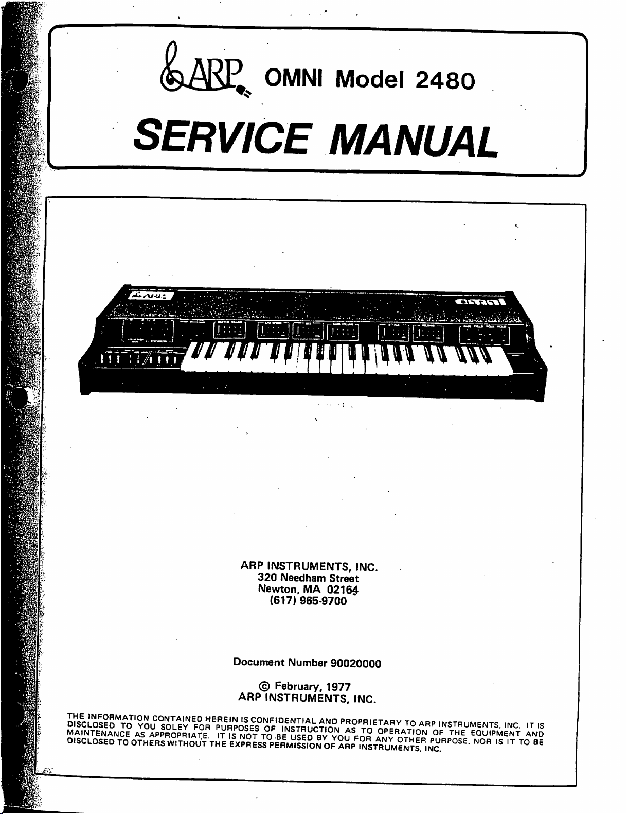
Page 1
;
Scan by Manual Manor
http://www.markglinsky.com/ManualManor.html
OMNI
Model
2480
SERVICE
MANUAL
CLOSeTt^^^^^
MAINTENANCE
O.SCLOSED
AS
TO
APPROPRIATE
OTHERS
ARP
INSTRUMENTS,
320
Needham
Newton,
(617)
Document
ARP
IT
IS
WITHOUT^
THE
NOT
'IxSSIJigSJKg&Sy
Number
©
February,
INSTRUMENTS,
TO
BE
uIpd
INC.
Street
MA
02164
965-9700
90020000
1977
INC.
Jv
vnn
cno
£PJRATI0N
Jw?!^,^^^*"**-
TO
ARP
0F
.NSTRUMENTS.
THE
EQUIPMENT
N°R
,NC.
,T
IS
AND
'S
IT
T0
BE
Page 2
OMNI
Scan by Manual Manor
http://www.markglinsky.com/ManualManor.html
Model
2480
SERVICE
TABLE OF
1.
INTRODUCTION
1.1
1.2
1.3
2.
THEORY
3.
CIRCUIT
3.1
3.2
3.3
3.4
3.5
3.6
3.7
Product
Specifications
Function
Upper
Lower
String
Synthesizer
Synthesizer
Phaser
Power
Description
Description
OF
OPERATION
DESCRIPTIONS
Voicing
Voicing
Control
Board
Supply
Board 5
Board
Board
Control
Board
Board 9
MANUAL
CONTENTS
2
2
3
5
6
8
10
10
11
4.
ASSEMBLY/DISASSEMBLY
5.
GENERAL
6.
CALIBRATIONS
7.
SCHEMATICS & LAYOUTS
8.
PARTS
INFORMATION
LIST
12
12
13
14-33
34-36
Page 3
Scan by Manual Manor
http://www.markglinsky.com/ManualManor.html
Page 4
[-»
Scan by Manual Manor
http://www.markglinsky.com/ManualManor.html
tiro
4—|
Swran r "*»■"
nnnnjnh
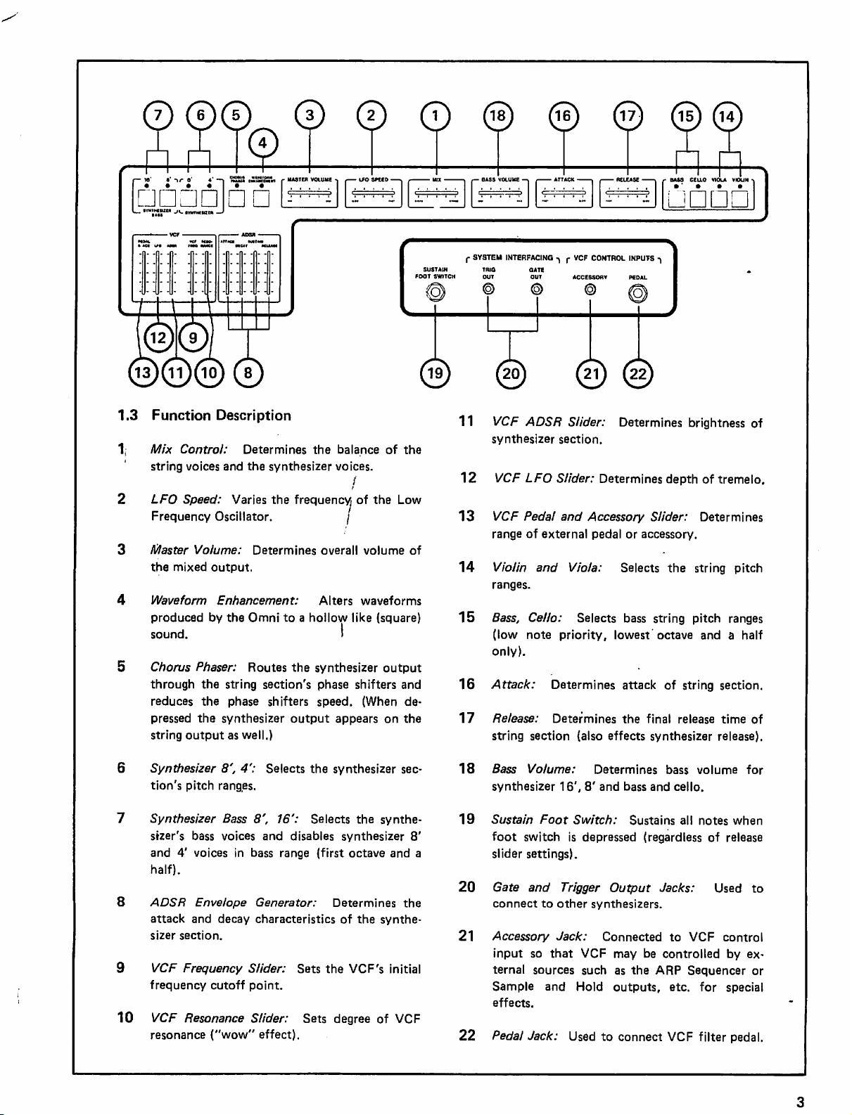
1.3
Function
1;
string
2
LFO
Frequency
3
Master
the
mixed
4
Waveform
produced
sound.
5
Chorus
through
reduces
pressed
string
Description
Control:
voices
and
Speed:
Varies
Oscillator.
Volume:
output.
Enhancement:
by
the
Phaser:
the
string
the
phase
the
synthesizer
output
as
[^
Determines
the
synthesizer
the
frequency
Determines
Omni
to a hollow
Routes
well.)
the
section's
shifters
output
volum
SUSTAIN
FOOT
SWITCH
the
balance
voices.
overall
Alters
>
synthesizer
phase
speed.
appears
of
the
of
the
Low
/
volume
of
waveforms
like
(square)
output
shifters
and
(When
on
de
the
18)
r
SYSTEM
INTERFACING
TRIG
OUT OUT ACCESSORY
11
VCF
synthesizer
12
VCF
13
VCF
range
14
Violin
ranges.
15
Bass,
(low note
only).
16
Attack:
17
Release:
string
(16)
•, r VCF
GATE
ADSR
section.
LFO
Slider:
Pedal
and
of
external
and
Cello:
priority,
Determines
Determines
section
(17)
CONTROL
INPUTS
PEDAL
Slider:
Viola:
Determines
Determines
Accessory
pedal
Slider:
or
accessory.
Selects
Selects
bass
string
lowest octave
attack
the
final
(also
effects
synthesizer
(15)
(14
-,
brightness
depth
of
tremelo.
Determines
the
string
pitch
pitch
ranges
and a half
of
string
section.
release
time
release).
of
of
6
Synthesizer
tion's
7
Synthesizer
sizer's
and
4'
half).
8
ADSR
attack
sizer
9
VCF
frequency
10
VCF
resonance
8\
pitch
ranges.
Bass
bass
voices
voices
Envelope
and
decay
section.
Frequency
cutoff
Resonance
("wow"
4':
Selects
8',
and
in
bass
Generator:
characteristics
Slider:
point.
Slider:
effect).
the
synthesizer
16':
Selects
disables
range
synthesizer
(first
Determines
of
Sets
the
Sets
degree
the
octave
VCF's
sec
synthe
and
the
the
synthe
initial
of
VCF
8'
a
18
Bass
Volume:
synthesizer
19
Sustain
foot
switch
slider
settings).
20
Gate
and
connect
21
Accessory
input
so
ternal
sources
Sample
effects.
22
Pedal
Jack:
Determines
16',
8'
Foot
Switch:
is
depressed
Trigger
to
other
synthesizers.
Jack:
that
VCF
such
and
Hold
Used
bass
volume
and
bass
and
cello.
Sustains
Output
Connected
may
as
the
outputs,
to
connect
all
notes
(regardless
Jacks:
to
VCF
be
controlled
ARP
Sequencer
etc.
for
VCF
filter
for
when
of
release
Used
to
control
by
ex
or
special
pedal.
Page 5
MASTER
Scan by Manual Manor
http://www.markglinsky.com/ManualManor.html
OSCILLATOR
1
line
TOP
OCTAVE
DIVIDER
J-LTL
12
lines
FREQUENCY
DIVIDERS
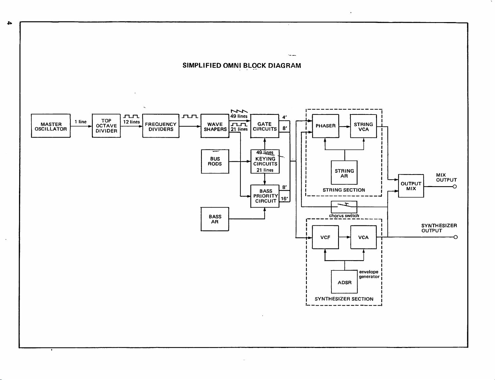
SIMPLIFIED
OMNI
49
WAVE
SHAPERS
21
BLOCK
lines
GATE
CIRCUITS
lines
DIAGRAM
PHASER
STRING
VCA
BUS
RODS
BASS
AR
KEYING
CIRCUITS
21
lines
BASS
PRIORITY
CIRCUIT
STRING
AR
STRING
I
VCF
j
SYNTHESIZER
SECTION
chorus
switch
a
ADSR
1
VCA
envelope
generator
SECTION
j
OUTPUT
MIX
MIX
OUTPUT
O
SYNTHESIZER
OUTPUT
O
Page 6

SECTION 2 THEORY
Scan by Manual Manor
http://www.markglinsky.com/ManualManor.html
The
OMNI's
master
scale
integrated
octave
the
instrument.
remaining
squarewave
a
sawtooth
the
waveshape
The
tones
transistor
string
section
tor
gating arrays
connected
(how
long
determined
input.
i
The
outputs
routed
section.
tone
generator
oscillator
divider
gating
to
at
500
circuit
produces
Frequency
pitches
to
from
outputs
form
from
the
by
the
of
each
(the
waveform
to a differentiated
the
waveform
arrays
which
and
the
synthesizer
are
'keyed'
each
key.
The
note
remains
the
release
of
all
the
gating
string
section
circuitry
kHz.,
top
octave
the
highest
the
top
divider
route
release
after a key
capacitor
arrays
OF
OPERATION
consists
which
drives a large
divider.
dividers
octave
are
enhancement
generator
the
section.
on
by
time
The
twelve
tones
derive
divider.
waveshaped
squarewave).
are
fed
signal
The
transis
an
RC
circuit
of
each
release)
on
each
are
summed
and
the
/synthesizer
of
a
top
in
the
The
to
alters
to
to
the
key
is
gating
and
The
string
section
shifters
from
processed
control
trolled
circuit).
The
the
Voltage
controlled
synthesizer
section
selected.
the
string
together
output
output
which
the
the
by
modulate
gating
through a Voltage
attack
the
"*
synthesizer
arrays
phasers
Chorus
section
of
is
section
through a Voltage
Controlled
by
an
output
when
The
speed
Phaser
and
in
the
the
instrument. A separate
provided
consists
circuits.
characteristics.
release
Amplifier,
ADSR
can
of
is
the
synthesizer
Mix
for
of
three
the
sawtooth
The
phaser
Controlled
(The
capacitor
processes
on
the
Controlled
both
Envelope
be
routed
through
the
Chorus
the
phasers
selected.
Circuitry
stereo
Phaser
is
The
section
and
effects.
parallel
waveforms
outputs
Amplifier
release
each
gate
outputs
Filter
of
which
Generator.
reduced
outputs
are
routed
synthesizer
phase
are
to
is
con
gating
of
and
are
The
the
string
Switch
is
when
of
the
summed
to
the
SECTION
3.1
Upper
GENERAL:
Master
Dividers,
Keying
ten
Gate
Keying
Lower
tics
for
3.1.1
(Refer
L1
and
approximately
tor
can
(externally
waveform
to
the
Scale
Integrated
highest
(C6-C7).
3
Voicing
The
Upper
Oscillator,
Wave
Circuits
Circuit
Circuits
Voicing
this
MASTER
DIVIDER
to
Q1
be
Top
octave
Top
Shaping
for
keys
I.C.'s.
and
Board. (Note:
board.)
OSCILLATOR
Upper
Voicing
produce a 0
500KHz.
varied
by
accessible).
from
the
Octave
Circuit)
(square
CIRCUIT
Board
Voicing
Octave
Gate
Master
Divider,
Divider
for
tones
21
through
The
remaining
I.C.'s
There
AND
Schematic,
to
—15
The
frequency
adjusting
Z1
the
buffers
Oscillator
Z2.
divider
waves)
which
DESCRIPTIONS
|
Board
contains
I.C.,
C7
through
49
and
Waveshaping,
are
located
are
two
TOP
sheet 1 of
volt
sine
of
the
core
of
and
squares
and
Z2
is a LSI
produces
of
the
instrument
the
Frequency
C4,
six
of
the
on
the
schema
OCTAVE
2.)
wave
at
oscilla
the
coil
the
supplies
it
(Large
the
3.1.2
(Refer
The
clock
which
wave
inverters
The
are
selected
the
resulting
DIVIDER
to
square
inputs
produce
outputs
AND
Upper
Voicing
wave
outputs
of
CD452OBE
square
of
the
Z9-Z16.
+v
Waveform
square
differentiated
negative
converter
waves
rrom
by
for
each
frequency).
portion
in
sawtooth
WAVE
SHAPING
Schematic,
from
Z2
are
divider
waves
for
each
key.
CD452OBE's
and
waveform
inverters
capacitors
of
the
differentiated
shaped
are
enhancement
Z9-Z13
C17-C49
CR1
through
waveforms.
CIRCUITS
sheet 1 of
supplied
chips
The
buffered
and
(values are
square
By
2.)
to
the
(Z3-Z7)
square
by
from
Z2
CR41
clip
wave
altering
Page 7

the
Scan by Manual Manor
http://www.markglinsky.com/ManualManor.html
DC
bias
(P6-7,
the
negative
permitted
Waveform
"hollow"
3.1.3
(Refer
Each
to a 22uf
resistor.
(The
When a key
to
—15
to 0 volts
be
varied
Control
key
(indicated
circuits;
portion
to
pass
Enhancement
type
sound.
KEYING
to
Upper
key
contact
electrolytic
The
capacitor
negative
side
is
depressed,
volts.
The
sets
the
by
the
Board.
one
The
by
for
8',
Waveform
of
the
through
Control
differentiated
diodes
is
selected
CIRCUITS
Voicing
(P7-5,
Schematic,
P7-4,
P7-3,
capacitor
is
normally
of
the
capacitor
the
capacitor
time
the
capacitor
release
time
release
letters
slider
key
voltages
KV)
one
for
are
4'.
Bus)
waveform
CR1-41
etc.)
through
charged
is
takes
of
each
(R31)
produced
supplied
when
resulting
sheet 2 of
is
connected
a
to 0 volts
at
—15
is
discharged
to
note
on
the
to
some
of
is
the
in
a
2.)
470ohm
volts.).
recharge
and
can
String
for
each
two
gate
as
the
inputs
used
for
4'
pitches
one
key
controls
The
Upper
arrays
the
Lower
base
pin
forms
resistor
pack
Z30
voltages
also
through
as
the
tor
remains
voltage
sistor
the
collector
cuitry
3.2
Voicing
and
three
Voicing
(7)
grounded.
are
supplied
(e.g.
Tone G 4
pins 5 and 6 to
(denoted
150Kohm
keying
voltage
off.
drops
in
the
array
of
(e.g.
from
Lower
Voicing
to
the
devices.
and
five
two
gate
Board
8'
arrays;
Board.
Each
to
an
emitter
by
KV)
resistors
is
at
When a key
to
—15
volts,
and
permits
the
array
pin
12
of
Board
Five
of
the
for
8'
pitches.
chips
at a time
contains
the
remaining
All
of
of
three
arrays
the
arrays
the
sawtooth
through a lOOKohm
is
supplied
pin
are
supplied
or
near 0 volts,
is
which
and
Z31
through
12
of
Z31.).
to
the
(e.g.
KV21).
depressed,
turns
on
the
signal
out
to
the
to
pin
14).
arrays
are
Therefore,
(4'
and
8').
4'
gate
are
on
have
the
wave
resistor
Keying
emitters
As
long
the
transis
the
keying
the
tran
to
pass
to
mixing
cir
KEY
CONTACT
BUS
ROD
J
-15V
Keying
3.1.4
(Refer
There
(TDA470)
tone
Gate
with
GATE
to
Upper
are a total
in
generator
has
ten
common
■15
470
ohm
3.3K
150K
22uf
t
-15V
100K
\
SAWTOOTH
WAVE
(TONE)
JL_
SUPPRESSION
TRIGGER
AND
STRING
RELEASE
CONTROL
and
Gating
CIRCUITS
Voicing
the
OMNI
sections
transistors
collectors
Schematic,
of
10
gate
which
to
the
(on a common
and
bases.
TDA470
TRANSISTOR
ARRAY
circuit
sheet 2 of
transistor
gate
signals
output
section.
substrate)
The
emitters
2.)
arrays
from
the
Each
serve
GENERAL:
Bass
Low
circuitry,
circuitry,
keys 1 through
G3#
and
3.2.1
The
Lower
Note
Priority
Gate
Sensing
8'
and
16'
20,
Gate
Waveshaping
WAVESHAPING,
CIRCUITS
(Refer
The
board
Voicing
detailed
3.2.2
(Refer
The
note,
lowest
through
fixed,
control
polyphonic
and
The
to
(only)
shaping
to
Lower
Voicing
Waveshaping,
are a
Board.
Gating
continuation
See
sections
descriptions.
BASS
to
8'
low
octave
the
generates
function
route the
in
LOW
Lower
Voicing
and
16'
Bass
note
priority.
and a half
20).
The
release
release
over
the
circuits
control
the
Bass
tones,
the
only
square
of
the
square
wave
Bass
section
(through
Voicing
Board
circuitry,
circuitry,
Bass
circuitry,
circuits
for
KEYING
Suppression
Keying
for
tones
AND
Schematic,
and Keying
of
the
circuits
3
1.2,
3.1.3
NOTE
section
Bass
PRIORITY
Schematic,
of
the
The
Bass
section
of
the
keyboard
time
of
the
on
the
front
section.
Bass
Unlike
Priority
waves.
Low
Note
of
the
lowest
to
the
8'
and
CR41-60)
contains the
4'
and
8'
Mixing
Trigger
circuits
tones
C2
through
C2
through
GATE
sheet 1 of
circuits
OMNI
Circuit
Priority
note
for
on
on
the
Upper
and
3.1.4
CIRCUIT
sheet 2 of
is
single
covers
(Keys
Bass
section
panel
has
the
4'
and
receives
circuit
depressed
16'
Bass
Wave-
processing.
for
G3.
3.)
this
for
3.)
the
1
is
no
8'
is
Page 8
The
Scan by Manual Manor
http://www.markglinsky.com/ManualManor.html
may
Bass
Waveshaping
only
accept
one
circuits
waveform
are
at a time.
monophonic;
they
(Z33-Z47)
keys
to
transmit
higher
than
the
one
serially
a
logic 1 state
depressed.
to
all
Square
Voicing
three input
outputs
only
Z33B
are
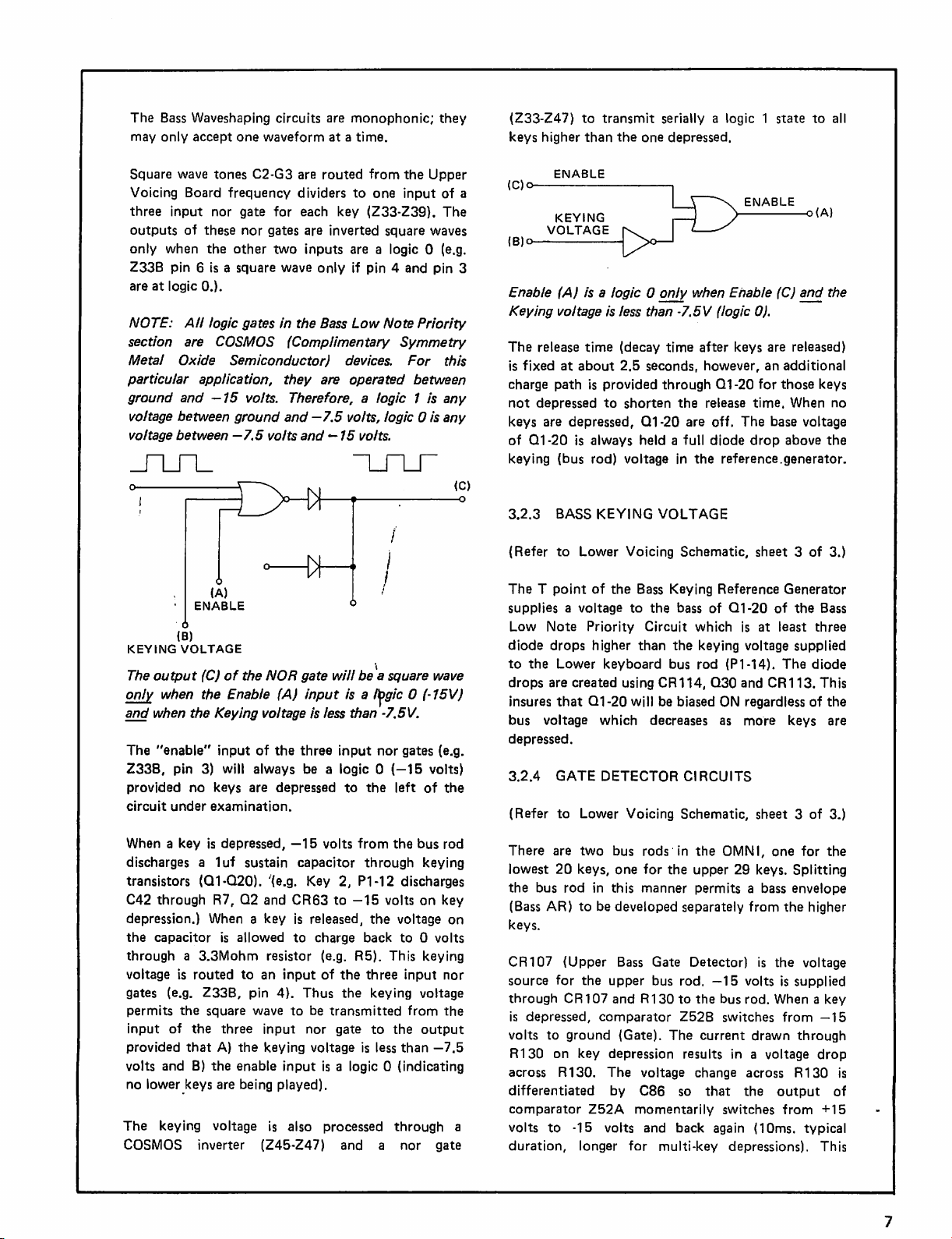
NOTE:
section
Metal
particular
ground
voltage
voltage
KEYING
The
only
and
The
Z33B,
provided
circuit
wave
tones
Board
frequency
nor
of these
when
the
other
pin 6 is a square
at
logic
0.).
All
logic
are
COSMOS
Oxide
Semiconductor)
application,
and — 15
between
between
(B)
VOLTAGE
output
when
when
"enable"
pin
under
ground
—7.5
(A)
ENABLE
(C)
of
the
Enable
the
Keying
input
3)
will
no
keys
examination.
C2-G3
are
dividers
gate
for
each
nor
gates
two
wave
gates
in
the
(Complimentary
they
volts.
Therefore,
and
volts
and
<—H
the
NOR
gate
(A)
voltage
of
the
three
always
are
be a logic 0 (—15
depressed
routed
are
inputs
only
Bass
from
the
to
one
input
key
(Z33-Z39).
inverted
square
are a logic 0 (e.g.
if
pin 4 and
Low
Note
Symmetry
devices.
are
operated
a
logic 1 is
—7.5
volts,
logic 0 is
-15
volts.
will
be a square
input
is a ibgic 0 (-15V)
is
less
than
-7.5V.
input
nor
gates
to
the
left
Upper
of
a
The
waves
pin
3
Priority
For
this
between
any
any
wave
(e.g.
volts)
of
the
(C)o
The
ENABLE
|B)o
Enable
Keying
is
charge
not
keys
of
keying
3.2.3
(Refer
The T point
supplies a voltage
Low
diode
to
drops
insures
bus
depressed.
3.2.4
(Refer
(A)
is a logic 0 oniy
voltage
release
fixed
path
depressed
are
Q1-20
(bus
BASS
to
is
time
at
about
is
provided
to
depressed,
is
always
rod)
KEYING
Lower
of the
Note
Priority
drops
higher
the
Lower
are
that
voltage
GATE
keyboard
created
Q1-20
which
DETECTOR
to
Lower
less
than
(decay
2.5
seconds,
shorten
Q1-20
held a full
voltage
Voicing
Bass
to
Circuit
than
using
will
Voicing
when
Enable
-7.5V
(logic
time
after
keys
however,
through
Q1-20
the
release
are
off.
The
diode
in
the
reference.generator.
VOLTAGE
Schematic,
Keying
the
bus rod
CR114,
be
decreases
Reference
bass
of
Q1-20
which
the
keying
(P1-14).
Q30
biased
ON
as
is
and
more
CIRCUITS
Schematic,
ENABLE
o{A)
(C)
and
the
0).
are
released)
an
additional
for
those
keys
time.
When
no
base
voltage
drop
above
the
sheet 3 of
3.)
Generator
of
the
Bass
at
least
three
voltage
regardless
supplied
The
diode
CR113.
This
of
the
keys
are
sheet 3 of
3.)
When a key
discharges
transistors
C42
through
depression.)
the
capacitor
through a 3.3Mohm
voltage
gates
permits
input
provided
volts
no
lower
The
keying
COSMOS
is
depressed,
a
1uf
(Q1-Q20).
R7r
When a key
is
is
routed
(e.g.
Z33B,
the
square
of
the
three
that
A)
and
B)
the
keys
are
voltage
inverter
sustain
Q2
allowed
to
the
enable
being
—15
volts
capacitor
'{e.g.
Key
and
CR63
is
released,
to
charge
resistor
an
pin
wave
input
keying
(e.g.
input
of
4).
Thus
to
be
transmitted
nor
voltage
input
is a logic 0 (indicating
played).
is
also
processed
(Z45-Z47)
from
the
bus
through
2,
P1-12
discharges
to
-15
volts
the
voltage
back
to 0 volts
R5).
This
the
three
input
the
keying
from
gate
to
the
is
less
than
through
and a nor
rod
keying
on
key
on
keying
nor
voltage
the
output
-7.5
a
gate
There
are
two
bus
rods
lowest
the
(Bass
20
keys,
bus rod
AR)
in
to
one
for
this
manner
be
developed
keys.
CR107
source
through
is
volts
R130
across
differentiated
comparator
volts
duration,
(Upper
for
CR107
depressed,
to
ground
on
R130.
to
Bass
the
upper
and
comparator
(Gate).
key
depression
The
by
Z52A
-15
volts
longer
Gate
bus
R130to
voltage
C86
momentarily
and
for
in
the
OMNI,
the
upper
29
keys.
permits a bass
separately
Detector)
rod.
the
Z52B
The
current
results
change
so
back
multi-key
from
is
—15
volts
bus
rod.
switches
drawn
in a voltage
across
that
the
switches
again
(10ms.
depressions).
one
for
the
Splitting
envelope
the
higher
the
voltage
is
supplied
When a key
from
—15
through
drop
R130
is
output
from
of
+15
typical
This
Page 9

pulse
Scan by Manual Manor
http://www.markglinsky.com/ManualManor.html
is
used
for
triggering
(ADSR)
not
3.2.5
(Refer
The
Priority
gated
and C77.
when
when a key
CR105
Z51A.
amplitude
couples
and
Q22).
samej(+7V).
rising
clipping
sawtooth
down
synthesizer
and
signal.
8'
in
for
provided
3.2.6
(Refer
The
clipping
key.
waveforms
+15
ground
off,
a
little
+15
about
NOTE:
output
more
input,
by
This
specialized
and
to
discharge
being
played.
8'
AND
16'
to
Lower
single
square
Circuit
through a "VCA"
no
to
As
the
the
8'
The
edge
off
(U2)
The
Bass
keys
are
is
depressed.
clip
the
the
AR
of
the
square
Bass
Waveshaping
base
and
This
of
the
the
falling
waveform
by
R114
Bass
signal.
resonated
The
square
half
(Z49).
the
by
16'
Bass
wave
from
CR106,
16'
Bass
as
with
the
WAVEFORM
to
Lower
Waveform
diodes
When
volts,
when
+15
volts
extra
volts
+13.5
Control
in
the
output
are
produced.
the
"hollow"
the
when
voltage
since
the
volts
by
The
CA339E
comparator.
negative
the
external
device
in
output
"pull
is
not a standard
comparator
BASS
Voicing
wave
is
AR
depressed
square
voltage
square
wave
emitter
means
squarewave
on
the
and
Q22
Waveshaping
Z51A
R119
circuit.
8'
Bass
CONTROL
Voicing
the
Waveshaping
Waveform
the
to
op
amp
itself.
When
voltage
is
open;
up"
resistor
(no
the
Envelope
sustain
capacitors
WAVESHAPING
Schematic,
from
buffered
made
voltage
and
This
voltage
wave
drops
wave
to
an
emitter
(R116,
of
that
only
will
edge
of
emitter
R174
The
sawtooth
and
used
and
and
Buffer
(Q23
Schematic,
sets
the
of
Z53
When
sound
Enhancement
switch
is
the
output
cannot
(Z52)
is
the
inverting
than
the
voltage
circuits
sheet 3 of
the
Bass
through
up
of
CR105,
(J11-8)
drops
to
sets
on
the
from
ground,
increases.
follower
C78,
Q21
are
the
differentiated
bias
Q21
the
squarewa've.
of
Q21
and
used/for
is
for
the
accepts
divides
the
the
C80
are
and
filtering
and
Q24)l
sheet 3 of
bias
point
circuits
is 0 volts,
the
output
is
produced.
on.
CR107
when
supply
an
open
input
the
noninverting
is
or
op
amp;
feedback).
Generator
on
keys
3.)
Low
Note
Z51A
and
R112
is 0 volts
—15
volts
the
bias
of
output
R117,
biased
of
the
C77
AC
(Q21)
C79,
the
on,
thus
The
is
divided
the
also
altered
string
bass
buffered
frequency
the
"VCA"
are
3.)
of
the
for
each
sawtooth
of
Z53
is
J11-9
is
switch
the
more
collector
determined
networks.
is
provides
input
is
than
(—)
is
(+)
it
is
a
The
Lower
Bus
Trigger
Bus
Gate
Detector
Bus
circuitry.
R150
creates
trigger
The
Upper
the
base
drive
circuit
common
each
key.
keying
from
running
maximum.
3.2.7
4'AND
(Refer
The
outputs
arrays
circuits.
instrument.
blocking
section
Bass
switches
Bass
controls
diodes.
The
4'
are
routed
theOMNI.
3.3
String
GENERAL:
String
AR
Squelch
Suppression
key
depressions,
times.
The
AR
to
capacitors
Voice
Selection.
3.3.1
(Refer
to
Z1
is a COSMOS
pitch
ranges:
bass.
Z3A
to
the
Phaser
Synthesizer
signals
Pins
1, 2 and
voices
are
CR112
the
voltage
on
key
depression.
and
Lower
of
Q27
and
and
sustain
discharge
The
trigger
capacitor
not
together
8'SUM
to
Lower
Voicing
of
the
(TDA470)
Formant
are
filtering
CR101,
diodes
which
(first
20
notes)
are
on.
are
on
Poly
Sum
(J11-16)
to
the
Control
The
String
Envelope
and
String
forces
yielding
AR
Squelch
be
the
same
by
tracking
STRING
and
VOICE
String
Control
Quad
4'
and
sums
the
Board.
section
for
processing
13
disable
selected.
Detector
circuit
are
is
the
difference
Bus
supplied
bus.
path
for
pulse
being
when
Schematic,
five
4'
summed
CR102,
disable
when
Z48
supplies
which
reverse
String
and
circuit
equivalent to
lower
bus
Triggers
via
The
the
keying
rapidly
played
the
and
8'
in
the
is
provided
CR103
the
outputs
the
8'
+15
biases
and
8'
Synthesizer
Board
Control
Generator,
Voice
Selection
the
AR
forces
as
the
release
the
audio
SELECTION
Board
Switch
8r
polyphonic
four
pitch
Z2
(pins
to
be
through
the
Board
AR
to
release
the
proper
the
release
time
level
Schematic.)
which
ranges
3,
4 and
summed
String
AR
and
Lower
the
Upper
voltage
source,
for
the
lower
bus
are
combined
Q26
to
sustain
capacitors
discharges
to
prevent
release
slider
sheet 3 of
gating
4'
and
to
and
CR104
of the
or
16'
Synthesizer
volts
the
Poly
Sum
sections
contains
Suppression,
circuits.
fully
string
time
of
all
from
the
selects
and
8'
and
routes
5)
permits
with
the
the
Phaser
when
on
the
pulse
bus
is
the
for
any
notes
is
at
3.)
transistor
8'
Sum
voice
the
are
bass
when
the
blocking
(J11-2)
of
the
AR
The
AR
between
attack
of
the
the
key
String
the
four
and
16'
them
the
String
Board.
no
string
Page 10

3.3.2
Scan by Manual Manor
http://www.markglinsky.com/ManualManor.html
STRING
(Refer
to
String
Control
The
String
control
VCA
on
integrating
no
keys
gate
signal
0
volts.
volts
which
rate
determined
released,
through
When a key
partially
remains
3.3.3
(Refer
Z4B
monitors
Voice
Z4B
and
(—15V)
reverse
charging
AR
voltage
which
the
Synthesizer
capacitor
are
depressed.
on
Z4A
Comparator
charges
by
the
—15
R37,
38, 39.
is
depressed,
discharge
from
previous
AR
SQUELCH
to
String
Control
the
audio
Selection
as
biases
circuit.
supplies
it
long
as
CR11
faster
than
AR
AND
Board
Envelope
controls
and
When a key
pin 6 changes
Z4A's
C15
the
volts
C15
key
Board
signal
C10
to
Z4C.
an
audio
and
the
AR
Schematic)
Generator
the
Control
is
Board.
normally
from
output
down
toward
attack
slider.
is
allowed
Q3
momentarily
to 0 volts
depressions.
Schematic.)
from
integrates
The
output
signal
prevents
decay
of
SUPPRESSION
produces
gain
of
the
String
C15
is
the
at 0 volts
is
depressed,
changes
—15
When a key
to
if
Z3A
the
of
is
present
the
AR
the*
audio
when
the
—15
volts
to
—15
volts
at a
discharge
turns
on
any
voltage
jn
the
String
output
Z4C
is
low
which
from
dis
signal.
a
to
is
to
of
volts
to
+15
volts
when
the
volts.
This
then
reverses
through
the
When
of
repeats.
3.4.2
(Refer
The
attenuates
gain
current
ADSR
(pin
trimmer
voltage
balancing the current
CR8
external voltages
through
3.4.3
(Refer
R45
and
the
direction
the
Z4A
SYNTHESIZER
AMPLIFIER
of
integration
output
switches
to
of
back
Synthesizer
Synthesizer
signals
of
the
supplied
output
3,
Z2)
(R14)
changes
and
R17
the
STRING
AMPLIFIER
to
from
VCA
is
to
the
is
connected
via
P12
minimizes
on
provide
from
output
jack.
VOLTAGE
Synthesizer
rate
Z4B
reaches
to
VOLTAGE
Control
Voltage
the
determined
differential
pin
the
through
output
entering
Control
output
of
Z4B
the
direction
control
—15
(R44)
at
the
output
—5
volts,
volts
and
CONTROLLED
Board
Schematic)
Controlled
output
10.
output
CONTROLLED
of
the
by
the
amount
pair
Z2A,
to
the
control
The
control
the
effect
Z2A
protection
the
Board
of
of
the
and
Z2B.
OMNI
Schematic.)
reaches
of
the
+5
current
and
thus
of
Z4B.
output
the
cycle
Amplifier
VCF. The
of
B.
The
input
rejection
control
VCA
by
CR7,
to
prevent
circuits
3.3.4
ADSR
BLANKING
The
ADSR
circuit
prevents
pedal
3.4
GENERAL:
the
Synthesizer
Oscillator,
String
Mix
and
3.4.1
(Refer
The
output
20Hz.
from
hysteretic
blanking
on
the
Synthesizer
the
ADSR
is
released.
Synthesizer
The
Synthesizer
Voice
Synthesizer
Voltage
Bass
LOW
to
LFO
in a frequency
Z4B
current
Controlled
AR
Envelope
FREQUENCY
Synthesizer
produces a triangle
and
C11
passing
switch
whose
provides a pulse
Control
from
triggering
Control
Board
when
Control
Selection,
Voltage
Amplifier,
Generator.
OSCILLATOR
Control
range
are
an
integrator
through
output
Low
Controlled
Board
and a square
from
R45.
switches
to
the
ADSR
board
which
the
foot
Board
contains
Frequency
Amplifier,
final
Output
Schematic.)
wave
about
.1Hz
to
which
charges
Z4A
is
a
from
—15
The
String
Voltage
circuit as
controlled
instead
3.4.4
(Refer
The
are
mixed
volume
3.4.5
(Refer
The
Polyphonic
audio
sizer
output
gates
selected.
the
Synthesizer
by
the
of
the
ADSR.
OUTPUT
to
output
of
MIX
Synthesizer
of
the
by
Z5A.
the
two
SYNTHESIZER
to
Synthesizer
four
pitch
range
and
8',
through
Control
of
(TDA470s)
Z1
Board.
the
first
when
Controlled
String
Synthesizer
R23,
signals.
VOICE
push
16'
to
the
CR5
20
notes
the
Amplifier
VCA
except
AR
Envelope
Control
the
Board
VCA
Mix
slider,
SELECTION
Control
Board
buttons,
4',
Synthesizer
VCF
input
and
CR6
disable
of
the
polyphonic
8'
and
16'
is
the
same
that
it
is
Generator
Schematic.)
and
String
VCA
controls
Schematic.)
8'
Synthesizer
Bass
on
the
the
route the
Synthe
the
audio
tone
pitch
ranges
are
Page 11
3.5
Scan by Manual Manor
http://www.markglinsky.com/ManualManor.html
Synthesizer
GENERAL:
Voltage
Generator,
Output
3.5.1
(Refer
to
The
four
and
16'
input
of
Voltage
Octave
The
filter
octave)
Z1B
sums
the
VCF.
trimmer,
audio
output
routed
to
3.5.2
(Refer
to
To
"start"
of
Z3A
(Logic
ADSR
Pulse
Drive.
with
no
keys
depressed.
input
(Z4D
and
Z4D.
will
cause
(logic
0)
volts
for
The
Pulse
and
pulses to
is
depressed.
but
drops
released
The
output
(0
volts)
Pulse
The
Controlled
ADSR
Processing
VOLTAGE
Synthesizer
pitch
ranges,
Bass,
are
the
VCF
Controlled
and
has a manually
accepts
on
pin 4 to
and
inverts
R22,
prevents
(pin
the
Synthesizer
ADSR
GATING
Synthesizer
the
ADSR
must
change
1
to
Logic
Gating
to
The
keys
depressed,
The
pin 13)
The
first
Z4C
to 0 volts
as
long
Drive
is
logic 1 (about
The
to
logic 0 when
to
prevent
of
Z4A
but
drops
Drive
pulse
Board
Synthesizer
Filter,
Gating
circuits.
CONTROLLED
Board
4'
summed
(pin
1,
M1).
Filter.
Board
ADSR
and
the
Schematic.)
and
8'
and
voiced
M1
It
has a cutoff of
variable
negative
the
control
control
control
external
CVR
the
voltages
(Control
voltages
10).
The
output
VCA
via
Board
Schematic.)
Envelope
Generator,
filter
from 0 volts
0).
Two
signals
set
up
this
condition:
Gate
(J12-7)
is
-15
and 0 volts
Gate
is
supplied
of
R-S
flip
flop
negative
pin
(logic
as
the
normally
ADSR
the
to
or
transition
10
to
change
1).
Pin
10
Gate
on
logic 0 (about
-1
volt)
blanking
the
sustain
ADSR
from
is,
therefore,
logic 0 (—15
the
ADSR
contains
the
Envelope
Gate
and
Trigger
FILTER
Polyphonic
is a 4075
Q
voltages
which
Voltage
from
of
J12,
to
must
volts
with
made
from
will
J12-7
every
is
normally
triggering.
normally
volts)
blanking
and
8'
on
the
audio
Low
Pass
24
dB/
(resonance).
(—1
volts/
cutoff
point.
control
Reset)
affecting
the;
pin
the
bejsent
the
one
to
on
remain
is
footswitch
the
VCF
is
output
—15
volts
to
the
Gate
and
(Logic
0)
or
more
the
Reset
up
of
Z4C
Z4C
pin
8
—15
volts
at
at 0 volts.
-13
volts)
time a key
logic
1,
logic
during
the
pulse.
0
is
1
second
output
3.5.3
The
negative
and
ATTACK:
high
R46
the attack
from
3 and
integrating
DECAY
following
of
turn
Z3D.
falls
—7.5
low
CR4,
turns
and
reverse
R51
RELEASE:
goes
on
Q6
input
the
release
setting
sustain
disabled
occurs
3.6
GENERAL:
identical
Low
responsible
OMNI.
Pulse
Drive
to
logic 0 to
ADSR
ADSR
the
to
to
ADSR
off
below
applying
R46
and
low
capacitor
to
sustain
Phaser
Envelope
going
DC
VCA.
When
low,
—15
the
noninverting
mode,
ground.
applies
Z2
—15
capacitor
AND
SUSTAIN:
the
voltage
voltage
and
R35
Z3C
and
Z3D
the
threshold
volts)
the
output
—15
R38
and
CR3
on
and
the
establishes
biased
and
CR5
to
the
When
which
turns
C13
ground.
of follower
time.
on
footswitch
whenever
The
and
decay
Q5
the
front panel
by
ADSR
the
Board
The
parallel
Frequency
for
the
directly
approaches
Z2
Oscillators.
will
momentarily
restart
the
ADSR.
Generator
voltage
the
volts
Q4
to
output
is
applied
input
is
off
follows
volts
through
C13
down.
on
capacitor
lowers
volts
the
is a bistable
of
of
Z3C
from
thus
voltage
capacitor
discharges
divider
the
Sustain
level
at
the
gate
on
Q6.
output
through
charge
and
Q7
to
is
depressed.
Release
footswitch
Phaser
Phase
Shifters
orchestral
circuit
control
of
Z3A
of
follower
and
R45
the
CR6,
Z1A
is a buffer
—10
volts,
voltage
latch.
the
changes
pin
holding
consisting
Level.
C13
discharges
Z2
pin
voltage
The
through
of
Z1A
R59
thereby
paths
from
permit
be
overridden
Pulse
Control
is
released.
Board
each
The
Phasers
string
force
Z3A's
provides
the
VCF
cutoff
changes
through
is
disconnected
voltage
R52
C13.
Q2
on
When
nand
from
10
of
Q2
off.
3.
is
removed,
remaining
R53,
is
applied
affecting
the
release
Drive
pulse
contains
from
CR2
and
Z2.
During
on
pin
to
charge
amplifier
The
output
begins
pin
13
pin
gate
(about
high
Z3
through
Q4
now
of
R45
CR6
is
now
through
Z3B
voltage
R50
and
to
the
preventing
the
slider
when
the
input
which
three
modulated
are chiefly
effects
of
the
a
to
of
13
to
is
by
Z3A
will
change
Z4C
has
changed
logic 1 as well.
until
after
10
Thus
the
from
to
logic 1 and
Z4A
Pulse
logic 1 to
after
delays
the
Drive
pulse
logic 0 then
Z4A
ADSR
has occurred.
when
changes
"starting"
to
A
3.6.1
(See
Oscillator
LFO
Section
3.4.1
circuit.)
for
details
of
the
Low
Frequency
Page 12
The
Scan by Manual Manor
http://www.markglinsky.com/ManualManor.html
three
Low
Frequency
modulate
to
Pin 1 of
clipped
R128
depressed,
3.6.2
(Refer
Voltage
used
Z104B
inherent
5
is
to
0
which
Z104A
should
oscillate
discharges
The Q output
oscillates.
Q102
current
the
of
Q101,
placed
modulation
varying
Q102-Q101.
3.6.3
(Refer
Z102
controlled
pins 2 and
be
out
the
Phase
.8msec.
Z105A
to
approximate
in
parallel
which
HIGH
FREQUENCY
to
Phaser
controlled
to
control
is a COSMOS
capacitance
pf)
as
the
timing
charged
maximum,
by
Q101.
the Q output
resets
the
is
used
Z104B
after
Z104B
and
Q101
converter
H.F.O.
the
square
of
R116
H.F.O.
102
to
in
parallel
when
the
depth
DELAY
to
Phaser
is
an
analog
by
12
waves
phase.
The
with
slows
Board
delay
one
to
cease
power
of
Z104A
are a linear
which
(calibrate)
The
vary
with
CIRCUITS
Board
the
(typically
Oscillators are
Shifters
is a triangle
capacitor
pin
varying
the
waveform
a
sinewave.
R127
when
the
down
the
LFO.
OSCILLATOR
Schematic)
High
Frequency
time
of
each
one
shot
which
of
COSMOS
on
T2.
Once
the
"capacitor"
(pin
10)
shot.
maintain
oscillation,
14
oscillation
or
up,
the Q output
to
start
Z104B
is a logic 1 as
voltage
determines
sets
the
sinewave
the
the
of
frequency
delay
frequency
of
the
audio
from
the
H.F.O.
R118
Schematic.)
exponentially.
to
increase
chorus
switch
change
line
whose
of
the square
50KHz.).
same
input
Pin
exact
of
the
used
to
delay
time
up
which
is
Z106B
The
the
connects
chorus
switch
is
Oscillators
phase
gates
are
shifter.
uses
the
(typically
capacitor"
is
charged
changes
initial
frequency,
to
logic
i
in
Z104B:
i^ot
begin
to
of
Z104
oscillating.
long
as
Z104B
to
exponential
frequency
of
frequency
LFO
controls
R119
is
the
depth
of
is
selected
produced
delay
2 and
device
by
by
time
wave
on
12
must
180
is
pin
is
3,
SUMMMING
the
outputs
Z103
frequency
are
Pin
13
is a latching
pulses
flip
from
CO.
3.6.4
FINAL
(Refer
The
outputs
by
Z1
Synthesizer
3.7
Power
3.7.1
Z1
contains a voltage
approximately
connected
an
op
amp.
an
emitter
controls
of
the
tion
of
of
the
op
amp
emitter
the
power
3.7.2
-15
The
—15
+15
volt
—
15
volt
of
R14
through
increase,
then
forces
lowering
3.7.3
SHORT
R7
and
limit
the
milliamps.
to a maximum
MIX
to
Phaser
Board
of
the
and
supplied
Board.
Supply
+15
VOLT
SUPPLY
+7
volts
through
The
output
follower,
the
pass
transistor
power
supply
R11
and
R12
op
amp
in
Z1
will
then
follower
volt
supply
supply
and
R2.
the
the
and
supply's
VOLT
SUPPLY
supply
through
is
R15
is 0 volts.
Should
voltage
Q2
to
output
CIRCUIT
the
transistor
+15
supply's
Q3
and
of
1000
three
pin 5
supply a correction
voltage
at
to
R5
AMP
OUTPUT
and
14.
flop
which
converts
Z104B
change,
will
with
pass
derives
the
the
on
supply
to
square
Schematic.)
Phase
Shifters
to
the
string
reference
to
pin 6 of
to
the
of
the
also
located
(Q1).
the
supply
the
transistor
to
normal.
R14.
When
correct
Z2
output
pin 2 of
more
—15
volts.
which
Z1.
noninverting
op
amp
Should
voltage
the
voltage
difference.
(Q1)
its
regulation
the
voltage,
is
referenced
of
the
Z2
also
current,
PRODUCTION
in
Z1
connected
current
limit
to a maximum
the
—15
supply's
milliamps.
the
high
waves
(Q
and
are
summed
VCA
on
the
supplies
This
voltage
is
connected
in
Z1,
the
at
the
inverting
voltage
and
from
output
the
to 0 volts
minus
increase.
is
input
of
to
which
output
junc
input
The
to
the
bring
the
of
the
junction
supply
Z2
thereby
to
pins 2 and 3
of
800
current
11
Page 13
SECTION 4 ASSEMBLY/DISASSEMBLY
Scan by Manual Manor
http://www.markglinsky.com/ManualManor.html
TUNE
CONTROL
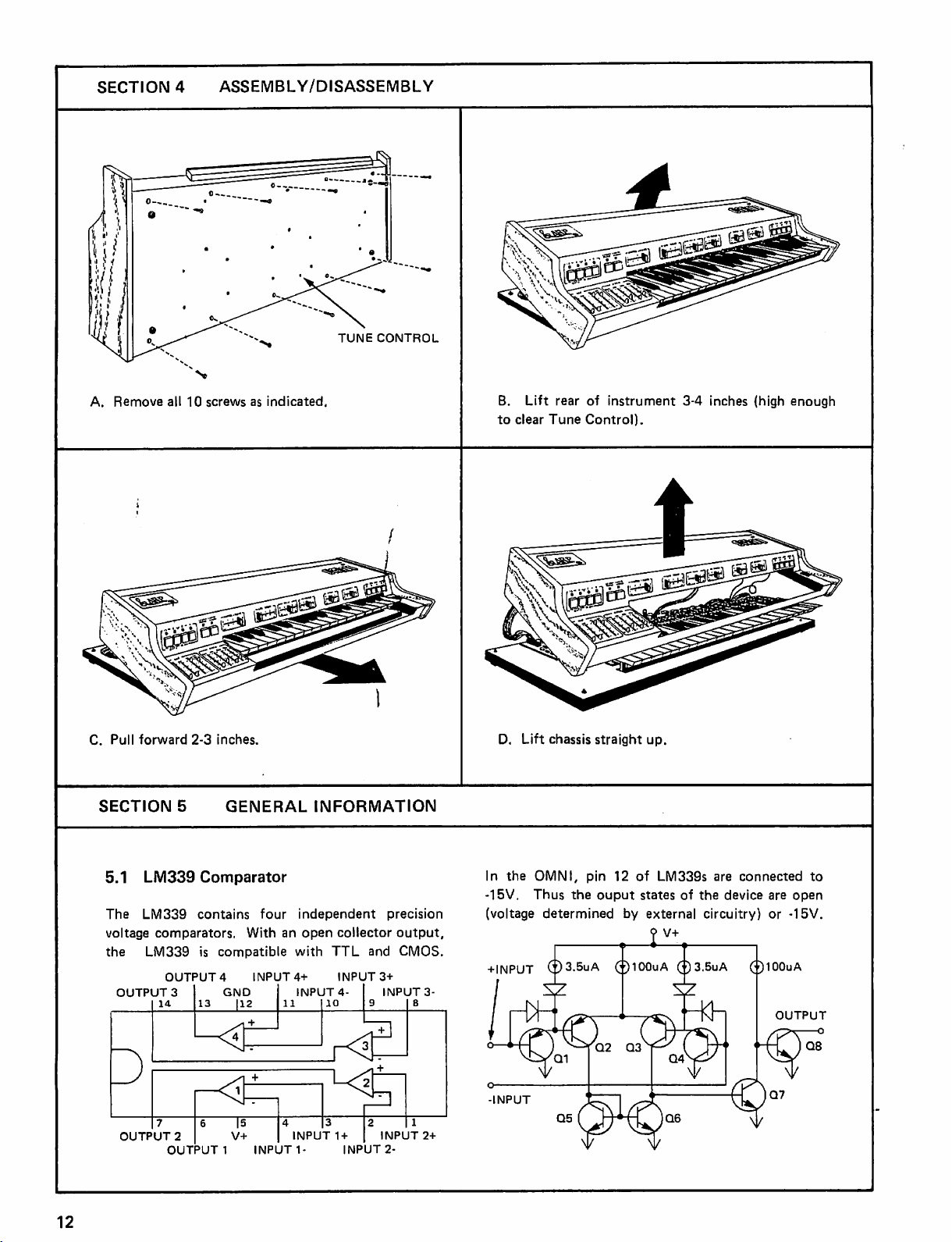
A.
Remove
all
10
screws
as
indicated,
B.
Lift
to
clear
rear
of
Tune
Control).
instrument
3-4
inches
(high
enough
C.
Pull
forward
SECTION
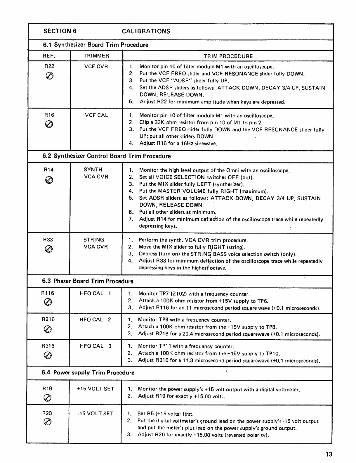
5.1
LM339
The
LM339
voltage
the
comparators.
LM339
OUTPUT
OUTPUT 4 INPUT
14
OUTPUT
OUTPUT
2-3
inches.
5
GENERAL
Comparator
contains
is
3
2
four
With
compatible
INPUT
1
INFORMATION
independent
an
open
collector
with
TTL
and
INPUT
4+
INPUT 4-I
11
10
1-
3+
INPUT
|9
INPUT2-
precision
output,
CMOS.
3-
B
D.
Lift
chassis
In
the
OMNI,
-15V.
Thus
(voltage
+INPUT
-INPUT
determined
Q3.5uA
straight
pin
12
the
ouput
by
(J)100uA
up.
of
LM339s
states
of
the
external
9V+
circuitry)
(J)3.5uA
are
connected
device
are
or
(J)100uA
to
open
-15V.
12
Page 14
SECTION
Scan by Manual Manor
http://www.markglinsky.com/ManualManor.html
6.1
Synthesizer
6
Board
Trim
CALIBRATIONS
Procedure
REF.
R22
R16
6.2
Synthesizer
R14
TRIMMER
VCFCVR
VCFCAL
SYNTH
VCACVR
Control
Board
1.
Monitor
2.
Put
the
3.
Put
the
4.
Set
the
DOWN,
5.
Adjust
1.
Monitor
2.
Clip a 33K
3.
Put
the
UP;
put
4.
Adjust
Trim
1.
Monitor
2.
Set
3.
Put
4.
Put
5.
Set
R16
Procedure
all
VOICE
the
the
ADSR
DOWN,
6.
Put
all
other
7.
Adjust
depressing
R14
pin
10
of
filter
VCF
FREQ
slider
VCF
"ADSR"
ADSR
sliders
as
RELEASE
R22
for
pin
ohm
VCF
all
other
for a 16Hz
the
MIX
MASTER
sliders
RELEASE
for
keys.
DOWN.
minimum
10
of
filter
resistor
FREQ
slider
sliders
high
level
SELECTION
slider
fully
VOLUME
as
follows:
DOWN.
sliders
at
minimum
TRIM
PROCEDURE
module
slider
follows:
module
from
M1
with
and
VCF
RESONANCE
fully
UP.
ATTACK
amplitude
fully
M1
pin
10
DOWN
when
with
of
DOWN.
sinewave.
output
of
the
Omni
switches
LEFT
fully
OFF
(synthesizer).
RIGHT
ATTACK
i
minimum.
deflection
of
an
oscilloscope.
slider
fully
DOWN,
keys
an
oscilloscope.
M1
to
and
the
with
(out).
(maximum).
DOWN,
the
oscilloscope
DECAY
are
depressed.
pin
2.
VCF
RESONANCE
an
oscilloscope.
DECAY
trace
DOWN.
3/4
3/4
UP,
while
UP,
SUSTAIN
slider
fully
SUSTAIN
repeatedly
R33
6.3
Phaser
R116
R216
R316
6.4
Power
R19
STRING
VCA
CVR
Board
supply
Trim
HFOCAL
HFOCAL
HFOCAL
Trim
+
15
VOLT
1.
Perform
2.
Move
3.
Depress
4.
Adjust
depressing
Procedure
1
2
3
Procedure
SET
1.
Monitor
2.
Attach a 100K
3.
Adjust
1.
Monitor
2.
Attach a 100K
3.
Adjust
1.
Monitor
2.
Attach a 100K
3.
Adjust
1.
Monitor
2.
Adjust
the
synth.
VCA
the
MIX
slider
to
(turn
on)
the
R33
for
minimum
keys
in
the highest
TP7
(Z102)
R116
for
TP9
with a frequency
R216
for a 20.4
TP11
R316
for a 11.3
the
power
R19
for
with a frequency
ohm
resistor
an
11
ohm
resistor
with a frequency
ohm
resistor
supply's
exactly
CVR
trim
procedure.
fully
RIGHT
STRING;
deflection
from
microsecond
from
microsecond
(string).
BASS
voice
of
the
octave.
counter.
+15V
supply
period
counter.
the
+15V
period
counter.
from
the
+15V
microsecond
+15
+15.00
period
volt
output
volts.
selection
oscilloscope
square
supply
squarewave
supply
squarewave
with
switch
(only).
trace
while
to
TP6.
wave
(+0.1
to
TP8.
(+0.1
microseconds).
to
TP10.
(+0.1
microseconds).
a digital
voltmeter.
microseconds).
repeatedly
R20
-15
VOLT
SET
1.
Set
2.
Put
and
3.
Adjust
R5
(+15
volts)
the
digital
put
the
meter's
R20
for
first.
voltmeter's
exactly
ground
plus
lead
+15.00
lead
on
the
volts
on
the
power
power
supply's
(reversed
ground
polarity).
supply's
-15
volt
output.
output
13
Page 15

£0W
Scan by Manual Manor
http://www.markglinsky.com/ManualManor.html
LEVSi.
PVASEPBD
7^//SO/
£xT
f/t
r£K
CONTJtei
ri
7Z/Z3O/
I
Sl
7Z//9O/
SWITCH
CONNECTION
V
fiZ
&YBOARD
\
OMNI
INTERCONNECTION
MODEL
2480
DIAGRAM
Page 16

fc I V
Scan by Manual Manor
http://www.markglinsky.com/ManualManor.html
rt n 13
^
*• ' l» 1 Ijl
---■■'>'
,'
fi\ * M
1..J
\
\
DESCRIPTION
FINAL
240V
FINAL
120V
FINAL
240V
ASSY
SEMKO
ASSY
CSA,
LA
ASSY
STANDARD
BRN
SWITCH,
BLK
SUPPLY,
BRN
SUPPLY,
TO
TO
TO
POWER
PIN
5
POWER
E-1
POWER
E-1
LINE
CORD
BLU
SWITCH,
WHT
SUPPLY.
BLU
SUPPLY,
CONNECTIONS
TO
TO
TO
POWER
PIN
6
POWER
E-2
POWER
E-4
GRN/YEL
GRNTOGND
GRN/YEL
TO
TO
GND
SCREW
GND
SCREW
SCREW
TO
POWER
BLK
SUPPLY,
BLK
SUPPLY,
PIN
TO
POWER
TO
POWER
POWER
2
SUP
E-3
E-1
E-1
CORD
PIN
TO
POWER
RED TO
SUPPLY,
RED
TO
SUPPLY,
CONNECTIONS
1
SUP
POWER
E-2
POWER
E-2
E-4
NONE
WHT
TO
SUPPLY,
WHT
TO
SUPPLY,
POWER
E-3
POWER
E-3
Page 17

MASTER
Scan by Manual Manor
http://www.markglinsky.com/ManualManor.html
(UPPER
UPPER
ffereooet—1
OSCILLATOR
VOICING
raeaucAiCY
UPPER
'Bits
to}
jxr
_n/
.
Si.)
BD)
Toetcs c "j
«vws
cz
ro
to c 7
as
->OOAR£
(lows*
nilff
toteiN6£t&
BASS
lunff/t
*
'BA**
finsfrff.tWTA
(carer
AK
lJ
yeHiMt
3e.)
vaci/t&Si.)
WAvf
iweiMSt
sei.eei
4-
voice
t
BO.)
en.)
3_r~
OMNI
MODEL
BLOCK
2480
DIAGRAM
Page 18

+
Scan by Manual Manor
http://www.markglinsky.com/ManualManor.html
ISV
P7-/6
P5-9
GND
P7-7
-/5V
"
1
C75
° > /o
1
T*
4>—mpn_£
At
,
L/
AS
/2K
22O4I*
2OX
/OK
/soop
<ai
2NS9/O
3*
C2
68OP
5%
C«7#
IW54A
CAT2
IM34A
|i
js
■-O
r
|b
|a
]»
|m
0°-
4 S 6 t a 9
|b
|io
H>
MKSO24CM
|»a
Z2
/O
// ( li
•♦
/*
/S|
?
29,'O.i/,
>a,ii,/*,iS,)tt
CO*O69ac
KCYIWS
T9W£
= TWO
VOLTA41
THACE
C*6
A/»^ffAA/*/«
*>IAC£S
21
PI.ACCS
ACS'STO*
CAPAC'TOA
O'OOCI
2.
19,'«,'','«,'3,'4.'J,'6
E
2ft,
3.
MiSMtST
4.
CO*/VC*/1~'O*/S
VOLTASC
VALUCI
VAC.
L/C
AAC
24.
23,26,2?,
ft
tt+*l+a
Kirocti
USS0
CO/
f
/AfPt/£S*(5Vf
i/MPnes
AflC
AAC
26
Ql,
Ql
-isv^
'/*
OMMt
>H
sUf
AAC
ARC
22K
CT5
,C«T2,42,J.I,
A/91C3
C"
PIT,
-TLTL
P6-/0
C»2
■
IBB A A
P6-9
C"3
fit?
ISA
CO452OM
C3
.0/
20a
•02
2OX
CT
.O5
2
C9
.O2
1
*
'1 TS
J-LTL
P*-/2
D2
iee
.as
toi
A6-/4-
£>3
m-TA.
CO4A2O8C
1%
t7
Ei%r
E.2C
12
Cll
C/8
.Of
02
20 x
20
1
1
I?
_TLTL
P5-/5
7
c/3
:
.os9
r.
!:
P6-/5
2
OK
J-LTL
£2
"P
r
«J2A Y V
2 e
C'S
C/«
•<va
*
.033 T ^e/
20R
2ox
I
:
£3
E/2O
C/7
hot
CtO
■02
_n_n_
P5-5
srj
P5-/6
C?O
.0/
2OK
1
'5
s
v
S6S
CD432OBC
C2/
■
O2
2OX
-TLTL
4
P5-/
5
I
y
C22
2OH
1 F 5
C2B
.O<
20X
1
S
C24
O/S
20»
-TLTL
P5-3
22
C25
.033
cox
r!
P5-2
G3
V
CZ6
.00M
20%
-TLTL
PS-8
r
.,«
C27
20X
czs
20%
C29
2O>
CM
Z0%
♦ b :r~
_n_n_
P5-7
A2
C32
.02
ZOX
!!»
E'OA
2
C53
:
.05-
20*
r?
9
yi/oo
a
C34
.005
: : .01 & .02
::?
ul
146
CO4S2OBC
\7
::?
_n_n_
P5-6
A»2
>«
4s
:i
C30
E98
C39
.01
20*
_TLTL
P5-/2
82
1 > m if
£9/
2
C-»2
.0/
2OX
P5-//
C2
B.SB
CO4S2O8C
C43
.02
!
20X
4.
4j
_TLTL
5
C3
AA"
CS
.OS
.005
30X
*
P6-7
COMTAOL
at/s
»aa-a
ma«*T
*a>2
11
mo |m
y
y
P6-3
■2*-:
1
P6-I
P6-I6
E£*-i
ECB-2
1
P7-II
P6-I3
P6-II
a.
Z26-S
E24
ia-6
1]
P6-2
P6-8
£26-
t99-
1
P6
-6
1
P6-4
P6-5
OMNI
PC
BOARD,
E24-S
MODEL
E3S-J
1
1
P7-I3
2480
SCHEMATIC
"UPPER
1
of
VOICING"
2
17
Page 19

*6O
Scan by Manual Manor
http://www.markglinsky.com/ManualManor.html
P7-I
RI7
J.9K
OV = short
CA42
—«
K&Y
2/
C**3
-M-
KEY
22
23
K£Y
CA4*
—M
cmr
—N—
e**a
CA5O
—W-
24
KEY
25
K£Y27
*£V2fl < J
release,
"P7-5
P7-4
,^
"PT-8
>3-/3
P3-/2
P3-9
-1SV ° long
47O
c4«
cso
cja
release
aa
asv
aa
aa
aav
aa
zsv
aa
aav
aav
-
3.3*
Cfl«a
MCY
KCV
cms*
CAA5
—w-
XEY
KB*
CAS7
K£V
m
KSV
C««9
■*-
CA*o
CA*/
—M
CA6a
CA4S
W-
"P3-8
3t
<
P36
I
32
P3-5
34 < J
33
<
I
P3a
36
P3-2
37 < I
P4-/3
^
I
P4-/2
P4//
P4-//
<
I
P4-9
1ST
47O
4
6
TO
9
aa
aa
cj?
aa
cjo
aa
car
za
aa
€*•♦ a a
aa
C64
aa.
c<>«»
aa
c«>7
aa
asv
t«v
13v
asv
»av
a«9
3.AM
—W
KEY
C«*fc
—m
M
KEY
CA*a
—W
CA7O
—N—
P-J-7
44
^
"P4-6
46 < I
P4-4
P43
P4-2
A4-/
139
C74
C73
C7/
cm
C66
22
22 25V
aa
asv
aa
a«v
aa
22
asv
25V
8'A
<JATC
Z53
TDAO4
OMNI
PC
BOARD,
MODEL
2480
SCHEMATIC
"UPPER
2
of
VOICING"
2
Page 20

OMNI
Scan by Manual Manor
http://www.markglinsky.com/ManualManor.html
PC
BOARD,
MODEL
ASSEMBLY
"UPPER
2480
VOICING'
19
Page 21

•si
Scan by Manual Manor
http://www.markglinsky.com/ManualManor.html
J
j
s:
23:
J
to
ltd
J
ar.
ttv
Irol
lull
KEY
I
KEY
2
PH2"
KEYS
«_J
PHI»
KEY
4
•
*4
PHO»
KEYS
«_J
J
v
Sir
g!
—
1
3<>
£w
IvJ
IodJ
-TLTL
J
K3
ft
J
J
J
LoJ [LJ
j
I
J
IU.J
luj
r 5 <n
I
J
3«
3
LqJ
J
J
J
LqJ
""v
0V/ + 15V
3
3
cawr/wt
|KV13>
=
voctasc
4'O
Af>f>£Af*lf*<i
J3-2
S
w»
,
TWO
CM
O/O0SS
2.
P/O, Q 3//
VALWSS
AM6
t**
A/7C
,,
C»«
CAt*
CR*O
KEY
7
KEY
8
KEY
9
pZp
KEY
10
KEY
II
KEY
12
KEY
13
u
KEY
14
2H2»
KEY
IS
KEYia
P2M01
KEYI7
£?
KEY
18
KEVI9
p
W«
KEY
20
P2H?
T
1
I
I
T
"aa
ca
"aa
aa
en
"aa
c«a
"aa
CIS
ltl5V
ci«
"aa
c/*
aa
c««
"aa
asv
cao"aa
cn
'zx
asv
asv
asv
aav
asv
tsv
aav
|KVI6S
kVI73
asv
asv
asv
20
short
release = 0V
long
release = -1
5V
J7-2
•f
fc
13V
OMNI
PC
BOARD,
MODEL
SCHEMATIC
"LOWER
1
of
3
2480
VOICING1
Page 22
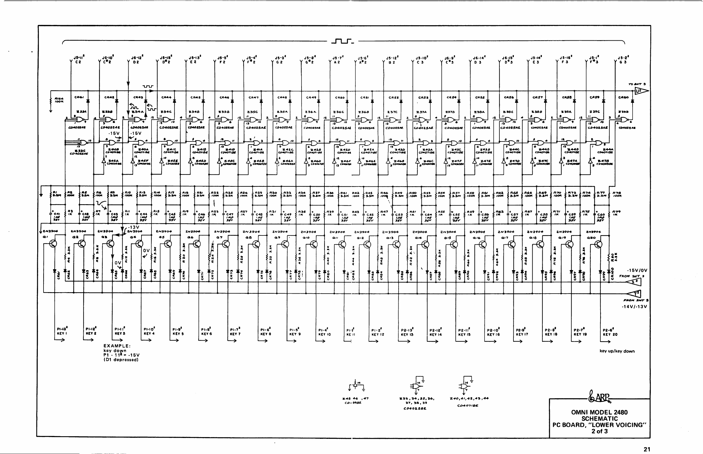
EXAMPLE:
Scan by Manual Manor
http://www.markglinsky.com/ManualManor.html
key
down
PI -11*=
(D1
-15V
depressed)
ZA/39O4-
an
(
a/2
I
key
up/key
down
S4S
♦*
co 4 wae.
,
IS)
,34,35,96,
37,
%B , 39
PC
BOARD,
OMNI
MODEL
SCHEMATIC
"LOWER
2
of
2480
VOICING"
3
21
Page 23

K
Scan by Manual Manor
http://www.markglinsky.com/ManualManor.html
synth
8',
16'
on = +15V
off = OV
u
-
•^
JBAS3T
POLY
DISABLE
)SSm
%%
-14.5V/-13.8V
-15V/OV
JH-7
>
»f
T
LMMUN
@2VP-P
Vf
<t'M
UPPER
BUS
TRICCER
OETECTOR
UPPER
BUS
GATE
OETECTOR
^
+6V
u:
-rt**
SUSTAIN
OVERRIDE
SUPPRESSION
~f
TRIGGER
GENERATOR
5*
"
+
15V
r*OM«MT
E>
•
i
JUL'
tone
Jlt-B
m'
arttrm
I
n
/
e'
sum
•-—JUL
0
6AS8
WAVE&HAPtNG
IP
«
CA»
"»
-14.5V/-13.8V
c*a^
J^
LOWER
TRIGGER
DETECTOR
<*«»*
BUS
«
PULSE
-
DRIVE
ov
-15V
m
C*ft
2?
C*T
JE
?2r
Ff
2VP-P
BASS
KEYING
**t
REFERANCE
*
*>
re
0V/+15V
CT1
S
mm
i
C^W
-
i -6
r»
2
o
1
«Tr
16'
BASS
WAVESHAPING
m;
:af
GENERATOR
WAVEFORM
I
•-
.«#
CONTROL
«■#*«
LOWER
BUS
GATE
DETECTOR
G*a * I
RiQ-t 4
J
1
Jll-S
/»■
ir*««
0V/+1
5V
key
up/key
down
PC
BOARD,
OMNI
MODEL
SCHEMATIC
"LOWER
3
of
2480
VOICING"
3
Page 24

,
Scan by Manual Manor
http://www.markglinsky.com/ManualManor.html
'I
Page 25

r
Scan by Manual Manor
http://www.markglinsky.com/ManualManor.html
Ji
w
plac£S
OMNI
PC
BOARD,
MODEL
ASSEMBLY
"LOWER
2480
VOICING"
23
Page 26
4*
Scan by Manual Manor
http://www.markglinsky.com/ManualManor.html
PELT
II'
Mil
Jt»-M>
Jl»-t4>
*.
%
STRIKE
VOICE
SELECTION
-*-
JaL
41
detects
audio
level
ah
souacN
0V/-15V
MIX
JlS-?>
A
-13V/0V
-$&
U-
A
AD5R
BLAKKIN5
5»
/"V
not
selected
OV
«+10V
to
H
i
I
AR
SUPRSSSIOM
0V/-15V
m
0V/-15V
TV
JL
^■?F;?;"'
a
•12V
1
^ I long
release
»
-15V
?
short
release
=
+8V
dc
dc
f
i
PC
BOARD,
OMNI
MODEL
SCHEMATIC
"STRING
2480
CONTROL"
Page 27

^Xge^a^Sya^/
Scan by Manual Manor
http://www.markglinsky.com/ManualManor.html
Page 28
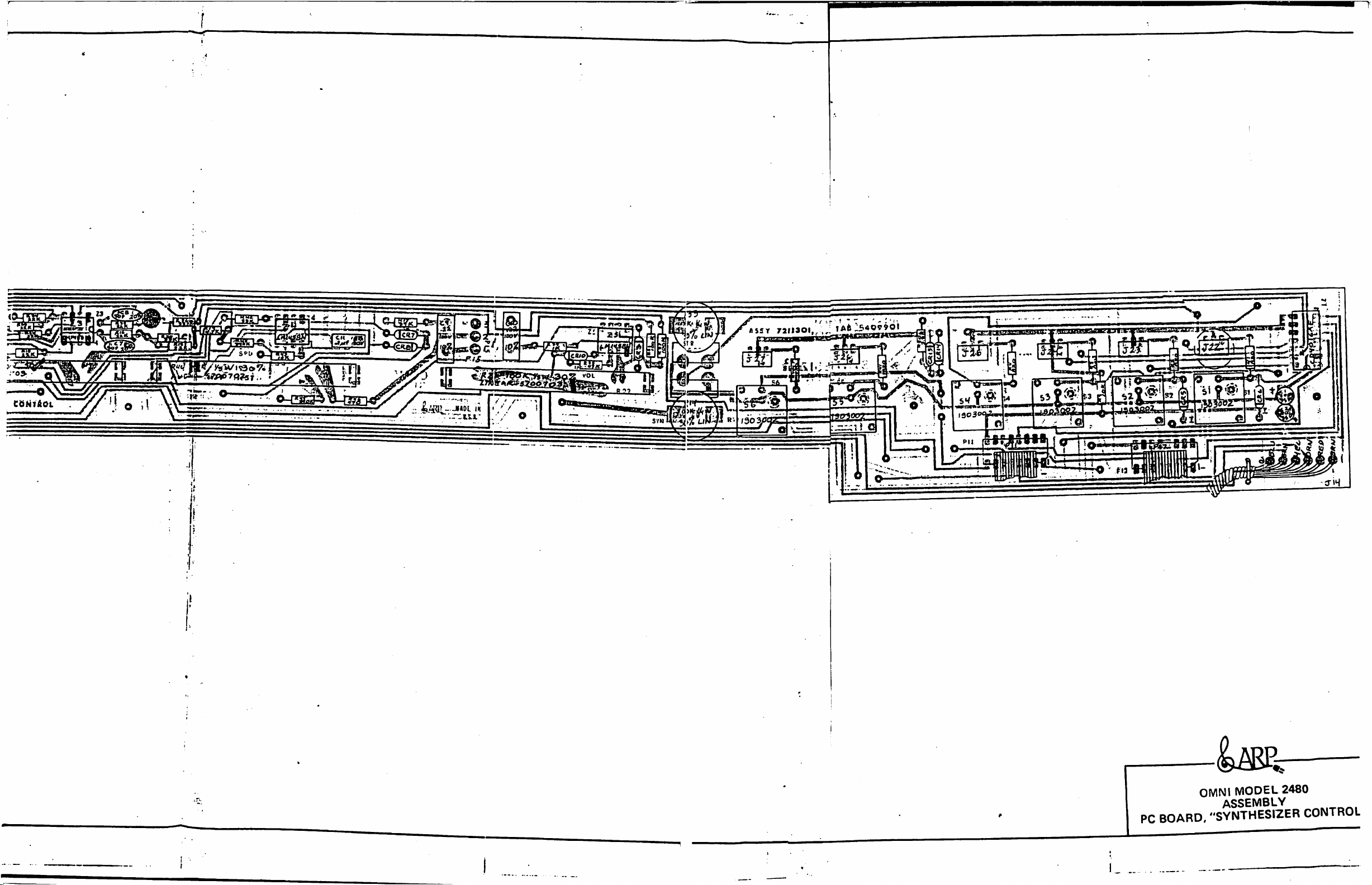
PC
Scan by Manual Manor
http://www.markglinsky.com/ManualManor.html
BOARD,
OMNI
MODEL
ASSEMBLY
"SYNTHESIZER
2480
CONTROL
Page 29

STRINO
Scan by Manual Manor
http://www.markglinsky.com/ManualManor.html
PC
BOARD,
OMNI
MODEL
ASSEMBLY
"STRING
2480
CONTROL'
25
Page 30

■1
Scan by Manual Manor
http://www.markglinsky.com/ManualManor.html
!•'
SHIM
tus uti
MIS
ri|-|l
ru-il<
JB2-1
SYMTHE51ZER
VOICE
SELECTION
J-LTT_
a
I
5TNTMESI2ER
VCA
->PI*-M
If
«OS
J
>^IH«
SfMTM
ffi
MS
CNULf
■<
1
!<
\
i<
1
rix-r
^...
/
««<—I
\
#IM<
1
'"^5—I
>«-<—'
n+ut
1
-15V/-13V
H
MSC
VIM
LOOCtJ*
TCHMCS
fOMDHLS
PC
BOARD,
OMNI
MOOEL
2480
SCHEMATIC
"SYNTHESIZER
CONTROL"
Page 31

VI
Scan by Manual Manor
http://www.markglinsky.com/ManualManor.html
3
>COj
Page 32

PC
Scan by Manual Manor
http://www.markglinsky.com/ManualManor.html
BOARD,
OMNI
MODEL
ASSEMBLY
2480
"SYNTHESIZER
CONTROL"
27
Page 33
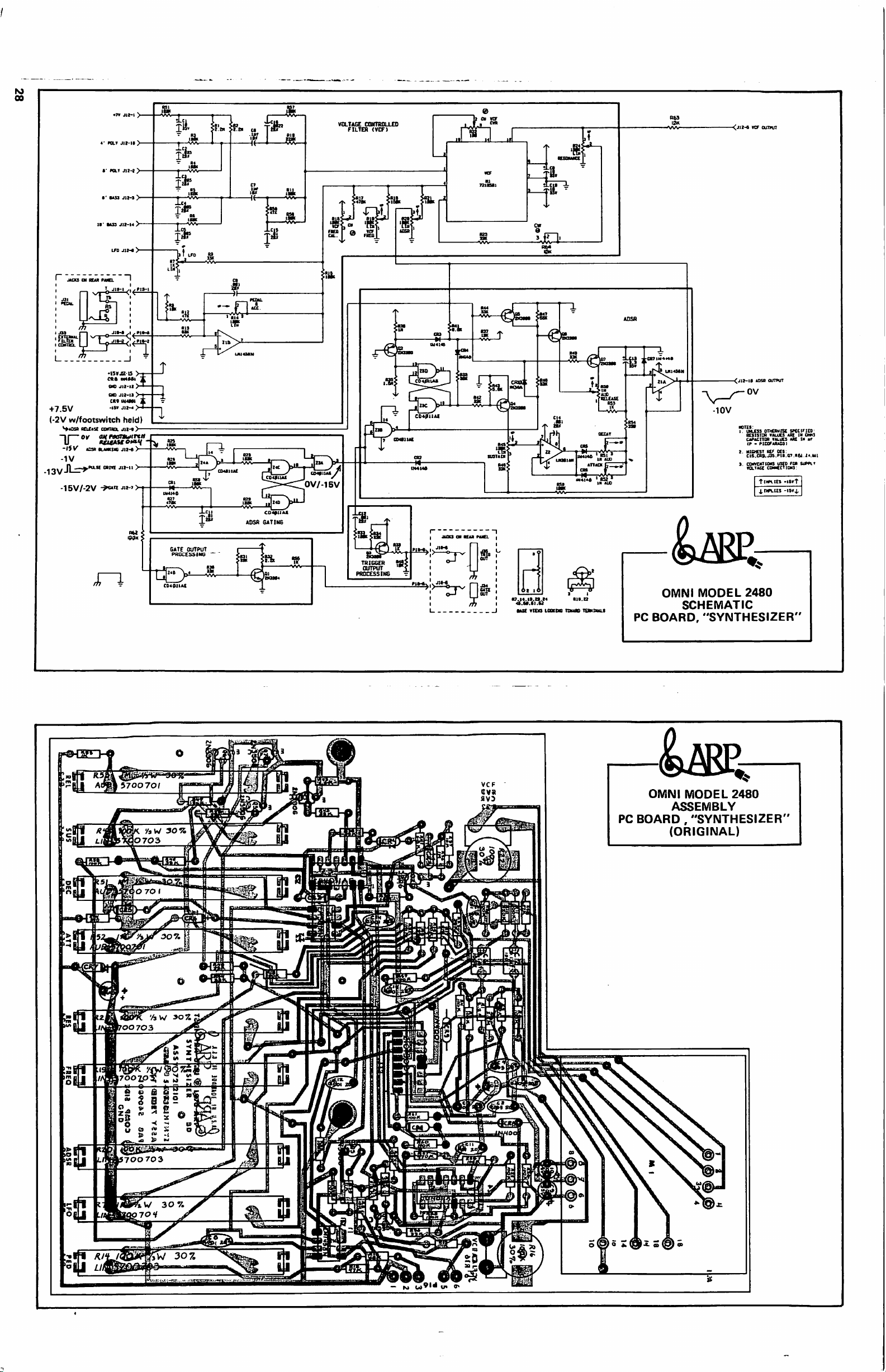
ro
Scan by Manual Manor
http://www.markglinsky.com/ManualManor.html
+7.5V
(-2V
w/footswitch
***osa
gome
coma.
held)
Jit-t
>-
<J!2-fi
VCF
OUIWT
OMNI
MODEL
2480
SCHEMATIC
PC
BOARD,
OMNI
"SYNTHESIZER"
MODEL
2480
ASSEMBLY
PC
BOARD . "SYNTHESIZER'
(ORIGINAL)
Page 34

OMNI
Scan by Manual Manor
http://www.markglinsky.com/ManualManor.html
PC
BOARD,
MODEL
ASSEMBLY
"SYNTHESIZER
2480
(REVISED)
Page 35
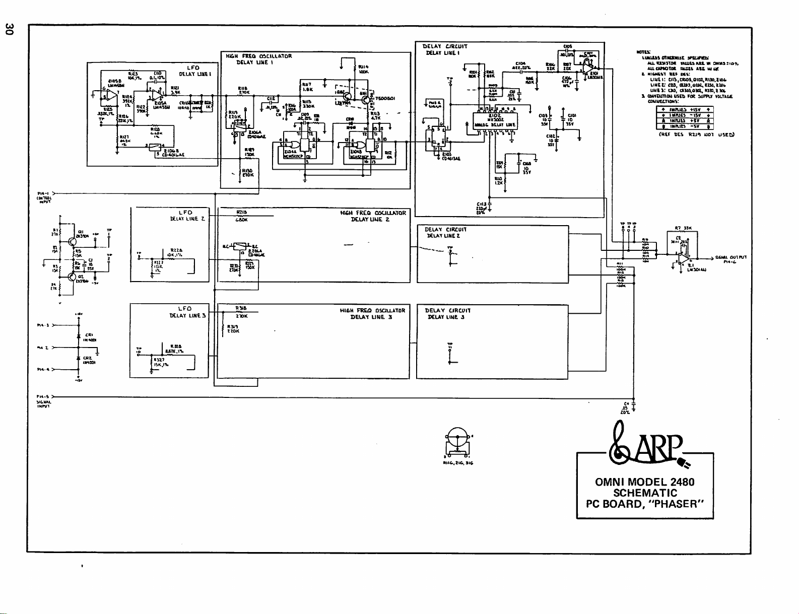
'life*
Scan by Manual Manor
http://www.markglinsky.com/ManualManor.html
LFO
OLLAY
rtilS
am
LIVE
I
El
Hl&H
DCLM
s»«
nt&O
(»CILLKTOR
UME
1
n
nous
M
LiHCt:
(twamw
COUHUTIOHV.
Ottf
cu,
auj1oiM,r2ia,iU(.
u«t»
for
CLi
RU1
MOT
USED)
LFO
DLUX
LIHt
Z.
J
LFO
DLLAY LINC3
J
ZTOtC
HI£U
FRED
DLLAYUME
HIGH
FRC^
O5CILLAT0R
Z
DSOLLATOR
UNE
3
DELAY
BELAY
DELAY
CIRCUIT
rr
t
LIME
3
ti
ssr
C4
T
OMIMI
MODEL
SCHEMATIC
PC
BOARD,
♦*
2480
"PHASER'
Page 36

OMNl
Scan by Manual Manor
http://www.markglinsky.com/ManualManor.html
ASSEMBLY
PC
BOARD,
MODEL
2480
"PHASER"
Page 37

^
Scan by Manual Manor
http://www.markglinsky.com/ManualManor.html
4
1 i
aliWR
OMNI
ASSEMBLY
PC
BOARD,
MODEL
2480
"PHASER"
.
Page 38
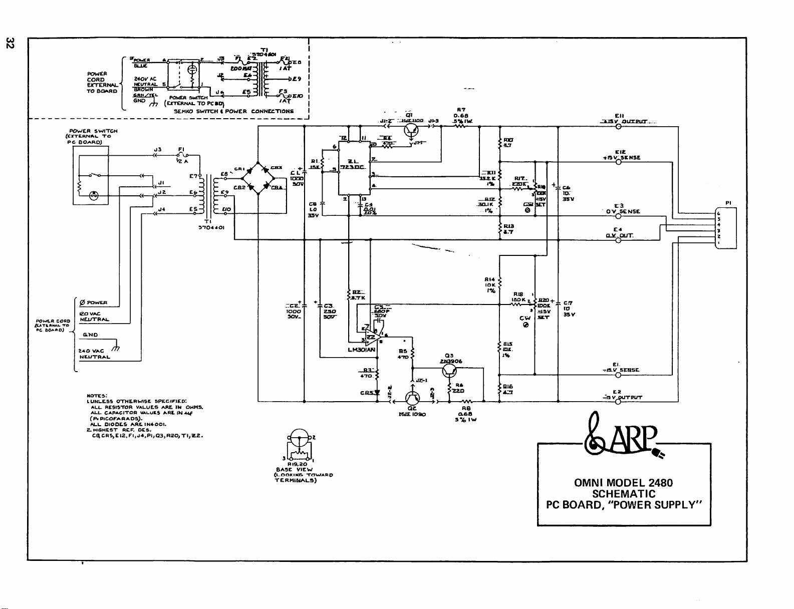
I
Scan by Manual Manor
http://www.markglinsky.com/ManualManor.html
POWtP
POWER
(CITTCRNAC
PC
BOARQ)
0
CORD
POWER
CORD
EXTERNAL**
TO
BOARD
SWITCH
TO
POWER
6ND
rh
(external
03
to
5EMKO
SWITCH t POWER
E5-
pcso)
CONNECTIONS
CL--
1
aov
LO
35V
i ± C3
r
RT
O.66
t
to:
1%
R13
RI4
IOK.
RIB
I0OK
-B2D
+
H7QK
to
35
cw
V
OV
E1C
E.3
SCNSE
O
ZAQ
VAC
NEUTRAL
'
NOTE5-"
L
UNLESS
OTHERWISE
AUU
RESISTOR
ALU
CAPACITOR
fP.
PICOFARADS).
ALL
DIODES
2.
HIGHEST
RCF.
VALUES
ARC
DCS.
4MLUES
SPECIFIED*.
IN4-OOI.
ARE
ARE
IKl
IN
OHMS.
AJf
BASE
VIEW
(l-OOKIMCi
TERMINALS)
HUEIO9C
HIS
IS
Blfi
OMNl
PC
BOARD,
£1
-J3.W
MODEL
2480
SCHEMATIC
"POWER
SUPPLY'
Page 39

OF
Scan by Manual Manor
http://www.markglinsky.com/ManualManor.html
06,7
8
OMNI
PC
BOARD,
MODEL
ASSEMBLY
"POWER
2480
SUPPLY1
Page 40
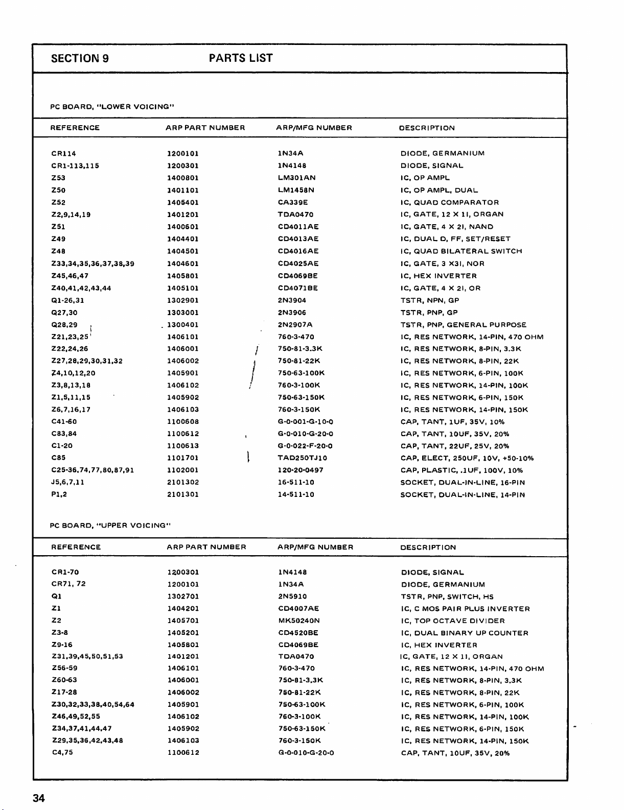
Scan by Manual Manor
http://www.markglinsky.com/ManualManor.html
34
Page 41

Scan by Manual Manor
http://www.markglinsky.com/ManualManor.html
35
Page 42
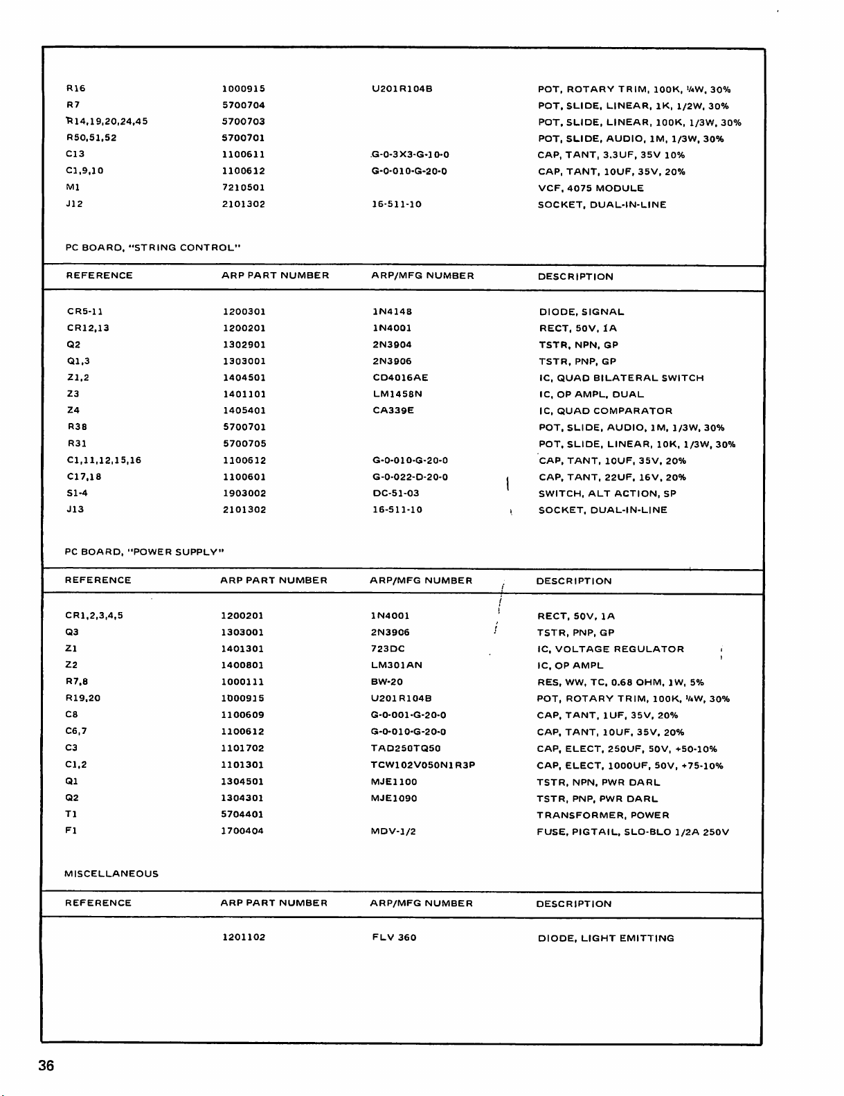
36
Scan by Manual Manor
http://www.markglinsky.com/ManualManor.html
Page 43

FOWCR
Scan by Manual Manor
http://www.markglinsky.com/ManualManor.html
CORD
EXTCRNAJ.
POWLR
4WITCM
(ClTLNNAL
PC
BOAftDl
TO
AB^V"
«WU»
/77
SWITCH1
^
Pi
UN1.CftS
OTHtBWlSE
ALL
RCUiTOR
(p.
PICOFARADS).
M.I.
DiODL*
BCF.
6PCCIFIC0*.
WAUOE.5
M»L
IN*OOI
QC».
ARt
IH
OMH*.
view
(U.OOKIM&
TCRMIMAL.fi)
TOWARD
QMNI
PC
BOARD,
MODEL
2480
SCHEMATIC
"POWER
SUPPLY*
Page 44

FCN0011
Scan by Manual Manor
http://www.markglinsky.com/ManualManor.html
series
'A'
series 'B'
REASON
CMOS
devices.)
FOR
MODEL:
EFFECTIVITY:
EST.
Please
failure,
CHANGE:
To
reliability
OMNI
TIME
TO
COMPLETE:
make
the
(This
Field
reduce
the
possibility
of
the
2483
SEE
following
Change
CMOS
BELOW
20
min.
changes
of
circuitry
to
any
Notice
is
not
transient
noise
when
instrument
DATE:
OMNI
that
necessary
from
for
power
is
11/14/77
is
being
OMNIs
supply
turned
repaired
for
a
containing
affecting
on
or
the
off.
PARTS
DETAILS
DISPOSTION:
OF
Order
FCN0011
CHANGE:
Refer
to
the
following
Refer
to
location
Readjust
It
series
power
is
recommended
where
possible.
parts
kit.
page
(Sht. 2)
of
components
supply
to
plus
and
that
defective
and
add
on
P.C.
Board
minus
CMOS
devices
the
components
assembly
13.00
volts.
be
(Sht.
replaced
as
illustrated.
3).
with
'B'
ARP
INSTRUMENTS
INC. ♦ 320
NEEDHAM
ST. ♦ NEWTON,
MASS.
02164 ♦ (617)-965-9700
 Loading...