

Arizona Microtek AZ100ELT21 User Manual
AZ100ELT21
Differential PECL to CMOS/TTL Translator
1630 S. STAPLEY DR., SUITE 125 • MESA, ARIZONA 85204 • USA • (480) 962-5881 • FAX (480) 890-2541
www.azmicrotek.com
ARIZONA MICROTEK, INC.
FEATURES
• 3.5ns Typical Propagation Delay
• Differential PECL Inputs
• CMOS/TTL Outputs
• Flow Through Pinouts
• Operating Range of 3.0V to 5.5V
• Direct Replacement for ON Semiconductor
MC100ELT21
• Use AZ100ELT21 for 10K Applications
DESCRIPTION
The AZ100ELT21 is a differential PECL to CMOS/TTL translator. Because PECL (Positive ECL) levels are
used, only V
CC
and ground are required. The small outline 8-lead packaging and the single gate of the ELT21 makes
it ideal for those applications where space, performance and low power are at a premium.
The ELT21 provides a V
BB
output for single-ended use or a DC bias reference for AC coupling to the device.
For single-ended input applications, the V
BB
reference should be connected to one side of the D0/D0¯¯ differential
input pair. The input signal is then fed to the other D0/D0¯¯ input. The V
BB
pin should be used only as a bias for the
ELT21 as its sink/source capability is limited. When used, the V
BB
pin should be bypassed to ground via a 0.01µF
capacitor.
NOTE: Specification in ECL/PECL tables are valid when thermal equilibrium is established.
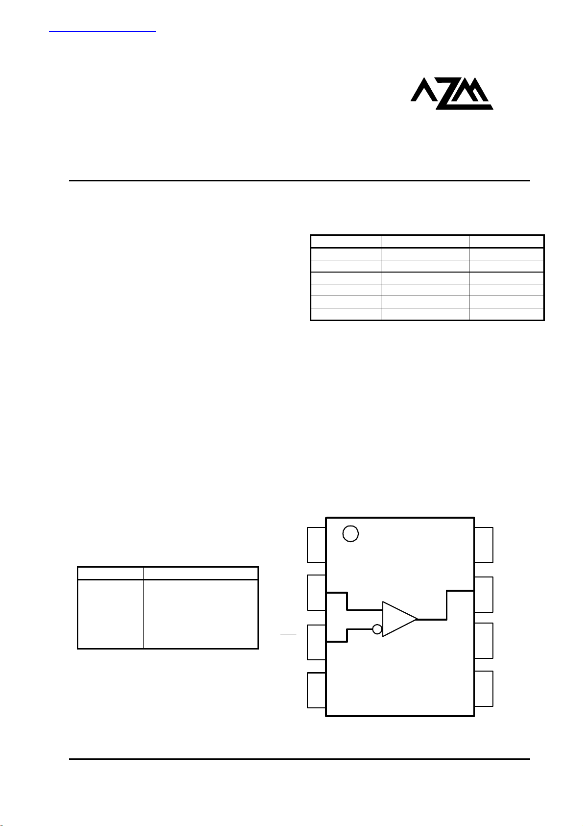
LOGIC DIAGRAM AND PINOUT ASSIGNMENT
PACKAGE AVAILABILITY
PACKAGE PART NO. MARKING
SOIC 8 AZ100ELT21D AZM100ELT21
SOIC 8 T&R AZ100ELT21DR1 AZM100ELT21
SOIC 8 T&R AZ100ELT21DR2 AZM100ELT21
TSSOP 8 AZ100ELT21T AZHLT21
TSSOP 8 T&R AZ100ELT21TR1 AZHLT21
TSSOP 8 T&R AZ100ELT21TR2 AZHLT21
PIN DESCRIPTION
PIN FUNCTION
Q CMOS/TTL Output
D0, D0¯¯ Differential Inputs
VCC Positive Supply
VBB Reference Voltage Output
GND Ground
NC No Connect
8
5
6
7
4
3
2
1
V
CC
Q
GND
NC
D0
V
BB
D0
NC
PECL
CMOS/TTL
查询AZHLT21供应商
AZ100ELT21
March 2002 * REV - 3 www.azmicrotek.com
2
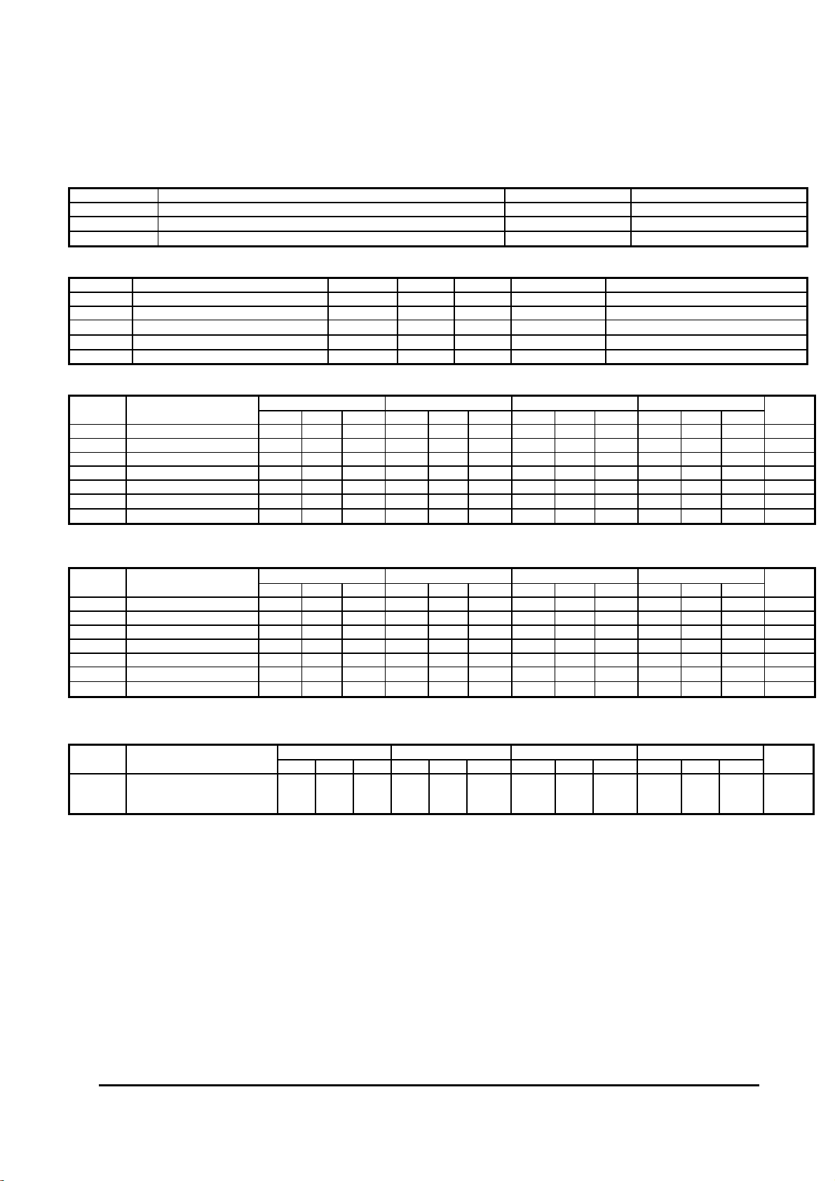
Absolute Maximum Ratings are those values beyond which device life may be impaired.
Symbol Character Value Unit
VCC DC Supply Voltage (Referenced to GND) 7.0 V
TA Operating Temperature Range (In Free-Air) -40 to +85
°C
T
STG
Storage Temperature Range -65 to +150
°C
CMOS/TTL DC CHARACTERISTICS (VCC = +3.0V to +5.5V)
Symbol Characteristic Min Typ Max Unit Condition
VOH Output HIGH Voltage V
CC
- 0.5 V IOH = -24 mA
VOL Output LOW Voltage 0.5 V IOL = 24 mA
ICC Power Supply Current
9.0 15 mA
0°C to 85°C
ICC Power Supply Current
9.0 17.6 mA
-40°C to 85°C
IOS Output Short Circuit Current 100 mA
100K LVPECL DC Characteristics (VCC = +3.3V)
-40°C 0°C 25°C 85°C
Symbol Characteristic
Min T
yp
Max Min T
yp
Max Min T
yp
Max Min T
yp
Max
Unit
VIH Input HIGH Voltage 2135 2420 2135 2420 2135 2420 2135 2420 mV
VIL Input LOW Voltage 1490 1825 1490 1825 1490 1825 1490 1825 mV
VBB Reference Voltage 1920 2090 1920 2090 1920 2090 1920 2090 mV
V
PP
Minimum Input Swing
1
200 200 200 200 mV
V
CMR
Common Mode Range 1.2 VCC 1.2 VCC 1.2 VCC 1.2 VCC V
IIL
Input LOW Current 0.5 0.5 0.5 0.5
µA
IIH Input HIGH Current 150 150 150 150
µA
1. 200mV input guarantees full logic swing at the output.
100K PECL DC Characteristics (VCC = +5.0V)
-40°C 0°C 25°C 85°C
Symbol Characteristic
Min T
yp
Max Min T
yp
Max Min T
yp
Max Min T
yp
Max
Unit
VIH Input HIGH Voltage 3835 4120 3835 4120 3835 4120 3835 4120 mV
VIL Input LOW Voltage 3190 3525 3190 3525 3190 3525 3190 3525 mV
VBB Reference Voltage 3620 3790 3620 3790 3620 3790 3620 3790 mV
V
PP
Minimum Input Swing
1
200 200 200 200 mV
V
CMR
Common Mode Range 1.2 VCC 1.2 VCC 1.2 VCC 1.2 VCC V
IIL
Input LOW Current 0.5 0.5 0.5 0.5
µA
IIH Input HIGH Current 150 150 150 150
µA
1. 200mV input guarantees full logic swing at the output.
AC Characteristics (V
CC
= +3.0V to +5.5V)
-40°C 0°C 25°C 85°C
Symbol Characteristic
Min Typ Max Min Typ Max Min Typ Max Min Typ Max
Unit
t
PLH
/ t
PHL
Propagation Delay to Output
1
VCC = 4.5V to 5.5V
V
CC
= 3.0V to 3.6V
2.0
3.5
5.5
7.0
2.0
3.5
5.5
7.0
2.0
3.5
5.5
7.0
2.0
3.5
5.5
7.0
ns
1. CL=20pF
 Loading...