

Page 1

Service
ARCAM
Bringing music & movies to life
DiVA
Manual
Issue 1.0
A80 Amplifier
P80 Power Amplifier
ARCAM
Bringing music & movies to life
Page 2

!
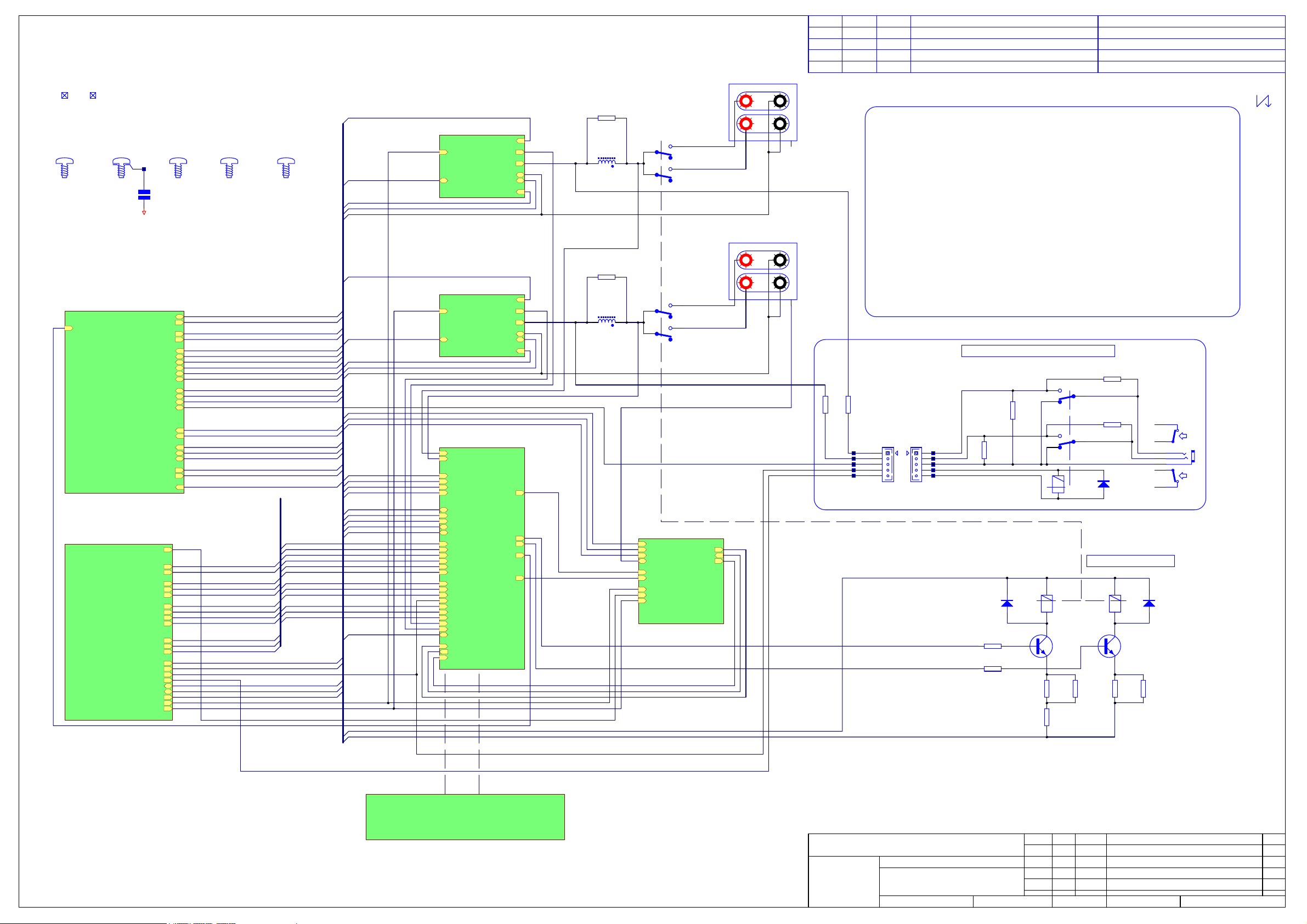
Circuit description
o
A80/P80
!
Technical specifications
Circuit diagrams
!
o L943AY
!
Transformers
o
L916TX – 115/230VAC toroidal
o
L917TX – 100VAC toroidal
o
L907TX – 100VAC frame
!
Exploded view diagram
o
A80
Mechanical & packing parts list
!
o A80
o P80
!
Circuit board silk screen
o
A80
o
P80
!
Circuit board parts list
o
A80/P80 combined
Contents List
Page 3
Circuit description.
Power supply.
The mains input to the unit is supplied at
filtered the Y Caps and locations C200 /C201 and X
cap at location C209, these are in-place to reduce
mains born HF interference and to prevent bridge
rectifier noise from leaving the unit.
The mains select switch at location
conjunction with the dual primaries on the 115/230v
transformers, the switch allows for the units to be used
in territories running a 115v or 230v grid when the
switch is set to the 115v position the primary windings
are connected in parallel.
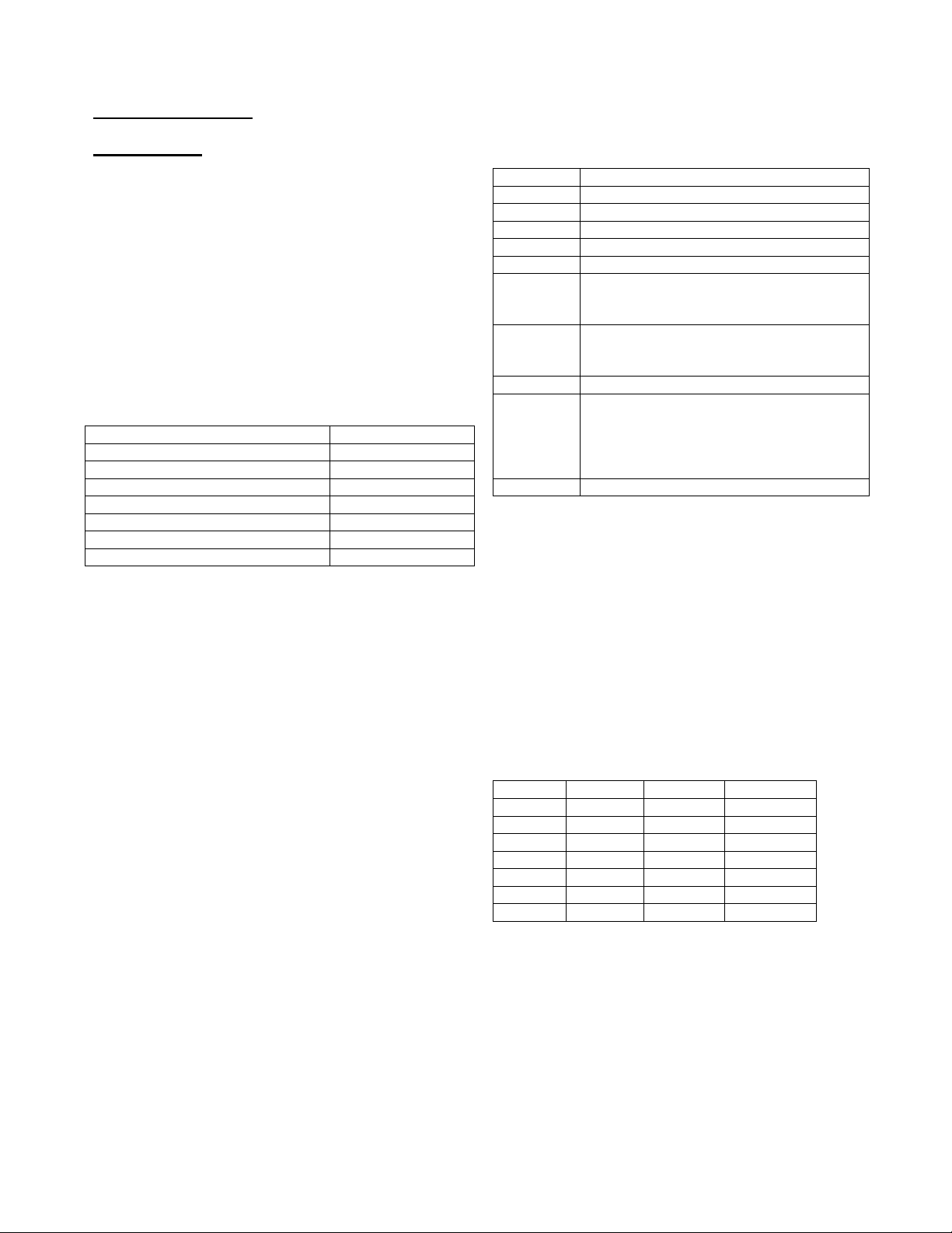
Fig 1. Fuse value information.
Fuse location. Value.
FS200 T2.5A (20mm)
FS201 T2.5A (20mm)
FS200 (100v) T3.15A (20mm)
FS201 (100v) T3.15A (20mm)
FS202 (s.m standby 9v a.c rms) T500mA (s.m)
FS203 (D.C inline) T2.0A (20mm)
FS204 (D.C inline) T2.0A (20mm)
The standby Transformer TX200 continuously powers
digital
the
connected to the unit, this supply powers the Micro via
a regulating circuit based around regulator
special mention should be made of fuse FS202 as any
interruption to this supply will render the unit
completely lifeless and as such this circuit should be
checked before inspecting any other areas of the
board.
We will see that the main power transformer
supplies a separate secondary winding for the
–15v analogue
board locations FS203 and FS204, the failure of either
of these fuses will cause the op-amps connected to the
regulated rails to swing D.C. The regulator at location
REG 200 regulates the +15 rail and intern supplies the
+5V(A) analogue supply via the reference Zener at
location
The high level power amp A.C supplies arrive at
Con204 as a 4-wire supply this allows us to implement
a dual bridge network circuit with 4 individually
smoothed D.C rails these are labelled as +45(L),
+45(R) and -45(L), -45(R) we pull a –38v rail from this
point to form the VFD cathode bias voltage via R211
Con205 delivers the 3.3 V A.C supply to the main
board and then onto the display VFD via R203 (2R2
f.u).
DZ200
circuitry (+4.8v(D)) when power is
regulation stages via the two fuses at
and drive transistor
SK200
and is
SW200
TR200.
works in
REG 201
TX200
+15
and
Fig 2. Supply identification and related components.
Supply Related components
+ 45v L
+ 45v R
- 45v L
- 45v R
- 38v VFD
+15v (A)
- 15v (A)
+ 5v (A)
+4.8 (D)
Fil 1/Fil 2
Left power amp positive rail.
Right power amp positive rail.
Left power amp negative rail.
Right power amp negative rail.
Display cathode rail derived from –45v(R)
IC 300, 301, 302, 303, 304, 305, 306,
307, 308, 309 also including the input
clamp diodes all within the pre-amp stage.
IC 300, 301, 302, 303, 304, 305, 306,
307, 308, 309 also including the input
clamp diodes all within the pre-amp stage.
IC309 volume control
Input trigger stages, signal detect IC700,
delayed off IC703, IC701. Main micro
IC600.Remote pickup, Master reset
IC601, Over current detect-AC detect –
thermal cut-out IC600
3.3v~ filament supply.
Pre-amp.
The A80 Pre-amp has inputs for Phono, Aux, CD, Tuner,
AV, DVD and Tape. All inputs except Phono have a simple
resistor-capacitor 340Khz low pass filter to remove any
unwanted high frequency noise from the input signal/local
area, a pair of diodes on each input connected to the
+15/-15v rails prevent damage to the CMOS input
switching chips at locations IC300 and IC301, if any offset
is seen at the input the switching chips on a given input we
may suspect the failure of one of the input diodes.
Fig 3. Logic status of IC302 and 303 (switching chip).
Low= 0V High=4.8 (Cmos).
Input. A0
Phono
Aux
CD
Tuner
AV
DVD
Tape
The outputs of IC300 (L) and IC301(R) can be seen on pin
8 as a current signal and such this can not be viewed via
CRO although a 100 ohm resistor inline with the scope
probe may yield some results, from here we drive into line
drive op-amp IC307 (L) and IC308 (R) signal can be seen
at the output pin (1) and travelling into the volume control
chip (IC309) on pins 16 (L) and 9 (R) the output from the
Volume control is driven into IC307 at pin 6 (L) and IC308
pin 6 (R) and seen again on pins 7 on both IC307 and
IC308. After the Con 302 and Con 303 we drive directly
(pin 1)
Low Low Low
Low High Low
High High Low
Low Low High
High Low High
Low High High
High Low Low
A1
(pin 16)
A2
(pin 15)
Page 4

Into the power amp stages but from this point we can
configure the unit as a separate Pre amp/Power amp
by moving the jumpers to the pin 2 and 3 of Con 304
and Con 305, and then remove the jumpers at Con
302 and Con 303 this may also be of use when fault
finding as we can effectively isolate the and D.C
offset/distortion problems coming from the Pre amp
stage to the power amp stages and test these stages
as a separate entity.
The Pre amp power up mute and power down mute is
controlled by the relay at location RLY300 A/B the
relay also triggers to mute the switching noise when
switching between inputs (see micro control/protection
and display section).
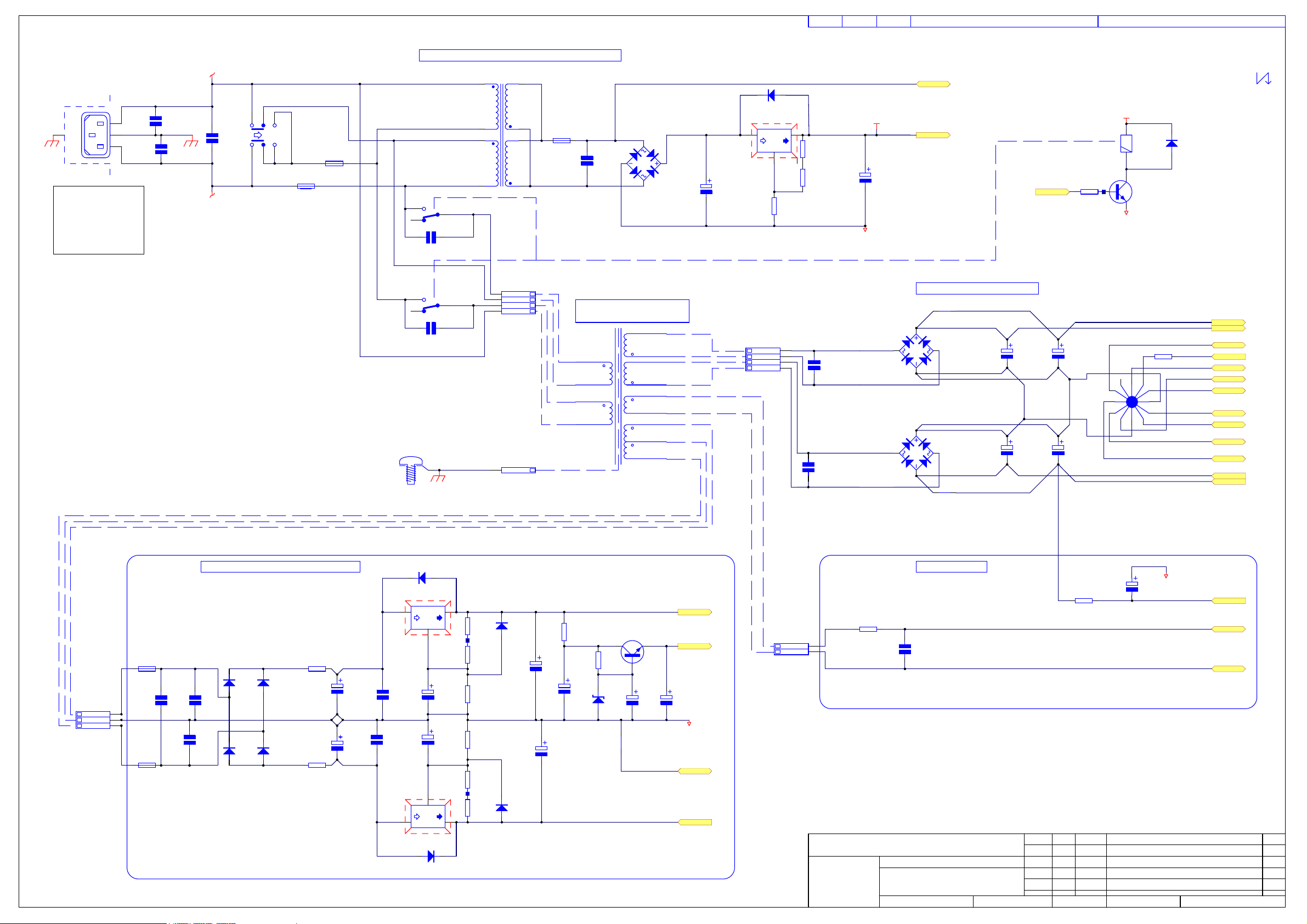
Power amp stages.
The main power amplifiers are of a Class A/B design
which use SAP “audio” transistors in a asymmetrical
current feedback configuration, Input and feedback
paths are D.C coupled and there is a active integrating
servo to remove D.C offsets from the outputs.
The basic principle of operation is as follows: Left
channel description given only, read all references as
5xx for the right channel.
The input level of the power amp stage is clamped by
the 3V9 zener diodes at positions DZ402 and DZ403
this protects the power amp input stages from gross
overload and subsequent damage R410 and R402 and
C416 in parallel form a 340khz filter.
IC400A is a V-I converter with a gain of 2 it’s output
will be a accurate amplification of it’s input voltage (i.e
the output voltage at pin 1 will be identical to the input
at pin 3 but twice the amplitude) the output voltage is
driven unto a 44 ohm load formed by R445 and R446
this op-amp is used in a slightly unusual configuration
in that it’s power supply pins are used as a current
output and the output pin is used as a current
feedback. Transistors TR404 and TR408 supply the +/15v rails and act as cascades to pass it’s supply pin
currents through to the current mirrors.
The “feedback current” flows back from the power amp
output via R447-R450 to allow IC400A to swing it’s
output, this is why the term current feedback is used –
it’s is the current flowing in the feedback resistors that
sets the overall gain of the amplifier.
IC400B acts as an inverting integrator and it’s purpose
is to remove DC from the loudspeaker outputs. Any
positive D.C offset will cause the output of IC400B to
go negative thus increasing the current in it’s negative
supply pin and pulling the output voltage back to zero
R420 and C442 set the time constant of the integrator
so that audio frequencies are ignored
The transistors found at locations TR400 and
TR401/TR402 form the PNP Wilson mirrors and TR416
and TR411/TR417 form the Wilson NPN current mirrors,
emitter degeneration is provided by R405, R406 (+) and
R407, R408 (-).
R415 and R416 decouple the current mirror stages from
the main power supply stages to allow the bootstrap circuit
to operate this circuit is formed by C423 and C424 and the
Metal film 1 watt resistors at locations R452/R453, the
boots strap is provided to allow the output stage rails to go
up and down slightly with the output signal to the
loudspeaker, this enables the driver stage to fully saturate
the output drivers giving the greatest output and the best
thermal efficiency.
TR405 and TR407 are the Pre-drivers, TR412/TR414 and
R411/R434 provide a current limit of about 30mA under
fault conditions. R423 and R428 loosely couple the
outputs of the output drivers to the inputs of the SAP
output devices, this allows the output devices inbuilt
temperature sensing diodes to accurately control the
quiescent current of the output drivers as the temperature
varies, C425 and C405 ensure that both halves of the
output stage receive an equal A.C component.
The output transistors are TR413 and TR415 these are
specially designed for audio power use Sanken SAP15N
and SAP15P devices they provide a inbuilt 0W22 thick film
power resistor and temperature sensing diodes that track
the V
BE
versus temperature characteristics of the power
transistors allowing for accurate control of the quiescent
current.
R459 and C427 form the Zobel network which is provided
to ensure that the amplifier see a constant and resistive
load at high frequencies C421 locally couples the “High
frequency” and signal grounds together at the input stage
for the same reason. Any signs of burning or scorching of
R459 will indicate that the unit amplifier channel(s) have
been running unstable or oscillating.
The Bias should be set for minimum distortion (THD+N)
using a 0.5v rms 20 Khz sine wave into the CD input with
the amplifier set for full gain, the absolute maximum level
of Bias acceptable is 22mV measure across CON401 (L)
or CON 501 (R) the adjustment is made using RV400 and
RV500 we set the bias at the factory using an extremely
accurate Audio Precision-audio analyser.
If you do not have access to a distortion level meter
capable of 0.05% or better accuracy you may be able to
rough set the amplifier to a typical reading of 15mV (at
cold switch on).
Page 5
Fig 4. Suggested blanket replacement parts for
power amp failures.
Location Description Model Part no.
TR413 Output driver + SAP15NY 4CSAP15N
TR415 Output driver - SAP15PY 4CSAP15P
TR410 Predriver + FMMT 497 4AFMMT497
TR412 Predriver + ZDT 6758 4AZDT6758
TR414 Predriver - ZDT 758 4AZDT758
TR405 Predriver - FMMT 597 4AFMMT597
TR401 Current mirror PNP BC859B 4A859
TR402 Current mirror PNP FMMT 597 4AFMMT597
TR411 Current mirror NPN FMMT 497 4AFMMT497
TR417 Current mirror NPN BC849B 4A849B
TR412 Driver bias + ZDT 6758 4AZDT758
Fig 4a. SAP NY/PY output driver information.
SAP 15NY SAP 15PY
Under output driver failure conditions the 0.22 internal emitter
resistor will usually go open, the resistor should be measured between
pins S and E.
S-E = 0.22 ohm.
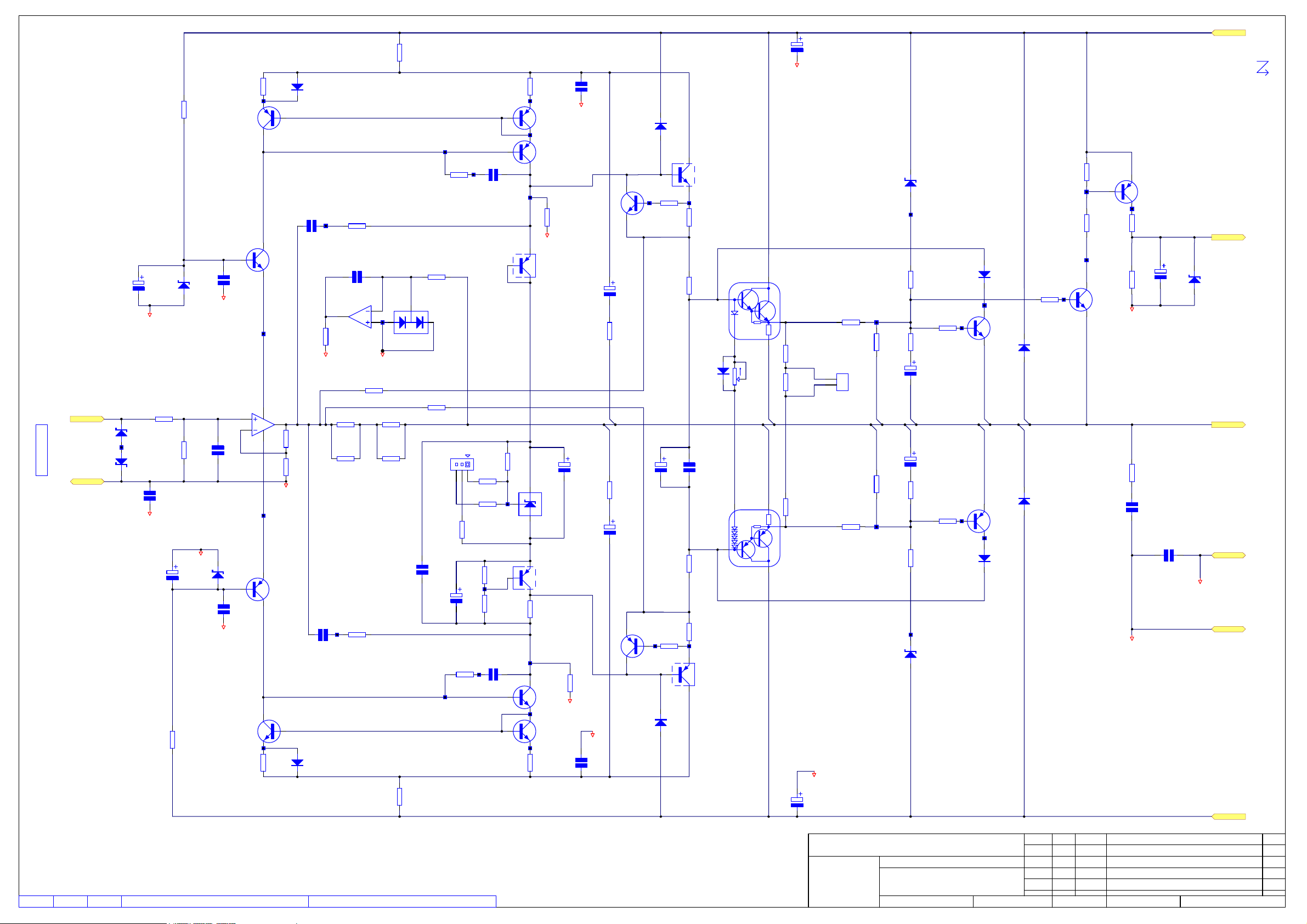
Micro control/protection and display.
The micro is tasked with providing an instantaneous safe
operating area for both the amplifier and loudspeaker by
monitoring the below areas.
o D.C
o Over current
o
at both left and right channel outputs.
within either power amp stage.
Over temp
detection for both power amp stages.
o A.C present detection.
Please see fig 5. For voltage readings with regards to the protection
operations.
Within the A80 integrated amplifier these tasks are
performed by the H8 type micro at circuit location IC602,
within the P80 power amp version the tasks are performed
by the PIC micro at location IC603, the protection lines are
“daisy chained” to both micros regardless of witch one is
fitted.
To operate both micros require a constant stable supply
voltage, this is derived from the
+4.8v(D)
rail from
transformer TX200 and via regulator REG201 this supply
should be constant at anytime mains appears at the
amplifier power input.
Please note: This supply is protected from over-current
and over-voltage operation by the surface mount fuse at
location
FS202
T500mA and as such if the Amplifier fails
to power up this supply should be checked before making
any further investigations.
We also need to see a
X600
.
4.00 Mhz
clock at crystal location
The micro interfaces with the pre-amp stage input
selection
(see Fig 3)
and the volume control level
adjustment we also drive the VFD via the display
drive/keyboard scan micro at location IC800.
IC602 receives Keyboard scan data and RC5 from the
remote pick-up diode at location RX800. The
power on
switches
reset
can be found on the display board and
HI
(4.8v) after mains in.
master
Fig 5. Working status of protection lines and fault
status
.
Low =0v High = 4.8 (Cmos).
Location Fault Line Output pin Working
IC 601A AC present 2 High
IC 600A Over current 3 Low
IC 600B Therm prot (L) 6 High
IC 600D Therm prot (R) 11 High
IC 600C Therm prot main 8 Low
R634 D.C prot (L) N/A Low (D.C)
R635 D.C prot (R) N/A Low (D.C)
R663 D.C prot combined N/A Low
Page 6
The Protection
is live at all times that even in standby
due to the fact that all chips related with these
functions are driven from the 4.8(D) supply rails.
As we can see from
Fig 4
we can isolate the left and
right channel protection lines for both over current and
D.C offset by looking at the protection lines before they
are mixed into single fault status lines for the micro at
location IC600 this will allow us to identify the channel
that is “flagging the fault”.
Both versions of the Amplifier have the ability to warn
the user and/or engineer of a internal fault, the A80 will
use both the Power LED and front panel display, the
P80 has no display and as such uses the sequence of
LED flash codes listed below in Fig 7.
Fig 6. A80 fault alert information.
Power LED status Fault indicated
LED red during start up DC offset fault
Led red during normal use Fault as shown on display
Fig 7. P80 fault alert information.
Power LED status Fault indicated
LED flashing green DC offset (left or right)
Flashing red Short circuit fault (over current)
Flash amber Thermal fault (heatsink L or R)
Red on flash green Multiple protection lines triggered
The Micro has direct control over all internal relays for
protection and output control, the speaker relay control
lines can be seen on the diagram as SPKR1 for SP1
and the SPKR2 for SP2 outputs, these lines switch
High to engage the relay.
The A80 pre-amp relay should disengage when
switching inputs to prevent any chip switching noise
from leaving the pre-amp stage the control line can be
seen on R385 and switches High to engage the relay.
Signal Detect and Delayed off – P80 only.
Signal detection is achieved by amplifying the signal
present at the power amp inputs by a large amount
using two channels of a quad op-amp at location
IC700 A/B the outputs of this op-amp are summed by
a non-inverting comparator formed using the two
remaining op-amp channels these will produce a active
High reset pulse at the output pin 14.
When mains is plugged into the P80, the master
*Reset line goes low and the 0.38Hz clock starts
ticking. The *Reset pulse resets the latch effecting a
HIGH *Q output and thus a LOW circuit output. When
the signal detect Latch and Counter Reset go HIGH
(an input is detected), the *SD latch input is driven
LOW by the inverter and *Q goes LOW the circuit
output then goes high switching the Amplifier on.
If the Amplifier does not see audio on it’s Power amp
inputs for either 12 or 45 minutes (this can be user
configured by moving the jumper at position CON702) the
Amplifier will auto switch into standby.
Jumper settings.
If you want to turn the A80 into a separate Pre-Power amp
(make the Line out become a Pre-amp out and make the
pre-out become a power amp in) adjust the setting of the
following links.
Remove the jumpers from Con 302 and Con 305 (this
disconnects the pre-amp output from the power amp input)
Fit jumpers on pins 2 & 3 of Con 304 & Con 305
(disconnects the line output buffer from the line out
sockets and connects the pre out sockets to the line out
sockets)
You can change the Phono input of the A80 into a AUX2
input by fitting jumpers on pins 2 & 3 of Con 306 an Con
307 this routes the signal directly from the Phono inputs
into a separate set of inputs on the pre-amp switches
IC302 and IC303.
We need to enable the AUX2 input by pressing AV,TAPE
and PHONO now use the rotary encoder to change the
selection, press confirm to select the new setting.
Con 400 and Con 500 are for the Bias setting and should
not be altered, if in doubt you should not measure more
than 22mV
across Con 401 and Con 501 when the
amplifier is idle and this should be adjustable using RV400
and RV500 (L&R channels).
Con 601 and Con 602 are for re-programming (move the
jumper from Con 601 to Con 602 when reprogramming
otherwise the jumper should be on Con 601).
Con 700 and Con 701 are used to set the P80 signal
detect sensitivity as default the link is fitted giving a input
sensitivity of roughly ~500uV if the jumpers are removed
the sensitivity decreases roughly x4 to 2mV this setting
can be used for operation with noisy source equipment.
Con 702 is used to set the time coefficient of the auto
power off delay, the default pins are 1 & 2 this gives a
delay of 12 minutes until the amp powers down under a no
signal period, if we place the jumpers on pin 2 & 3 this
time increases to 45 minutes +/- 20%.
Fig 8. Jumper settings.
Jumper A80 P80
Con 300, Con 301 Not fitted Fitted
Con 302, Con303 Fit (NF for pre/pwr) Not fitted
Con 304, Con 305 1&2 (2&3 for
pre/pwr)
Con 306, Con 307 1&2Phono;(2&3
Aux2)
Con 400,Con 500 Factory set Factory set
Con 601 Fit (NF to program) Not fitted
Con 602 Fit (NF to program) Not fitted
Con 700, Con 701 Not fitted Fit (0.5mv), NF (2mV)
Con 702 Not fitted 1&2 (12 mins; 2&3
Not fitted
Not fitted
45mins).
Page 7
Fig 9. Major components pin identification.
74HC14
TLO 72
ZDT 758/ZDT 6758
1=Collector 1
2=Collector 1
3=Collector 2
4=Collector 2
5=Emitter 2
6=Base 2
7=Emitter 1
8=Base 1
FMMT 497/597
NJM2114
DG408DY
74HC00D
BC849/BC859
3=Collector
1=Anode
2=Cathode
3=Common connection
1=Base
2=Emitter
BAV99 Diode package
LM431 Adjustable Zener shunt regulator
Page 8

Technical Specifications.
Continuous Power output
Both channels driven 8 ohms 20 Hz – 20 kHz = 65 Watts
Single Channel driven 4 ohms 20 Hz – 20 kHz = 80 Watts
Distortion 8 ohms at 80% power output 1Khz = 0.008%
Input stage specifications.
RIAA input stage sensitivity (M.M) = 2.5 mV
Line input sensitivity = 630 mV (Default)
Input impedance = 22k ohms
Signal to noise ratio CCIR weighted (2 volt input) = 105dB
Pre-amp output specifications.
Nominal output level = 610 mV
Output impedance = < 3 ohms
Page 9
FD100 FD101
LS100
G P PRECISION
Left Outputs
ITEM100 1 Blank PCB Diva A8 0 AmpL943PB
ITEM101 1 Tape D/Sided 12MM X 70MM DS Polyester 4965F205 Placed between VFD and PCB; NF ON P80
ITEM102 1 Earth Lead Assy 75MM8M101
ITEM103 2 Pad Damping 15x6x3MM SorbothaneE802AP
ITEM104 4 13/16 inch O-RingF232
Soldered to SKT200
Placed on output relays
Rubber O-Rings fitted over main power supply caps
ANNOTATION
FIX100
Dia 3.5mm
Power Supplies
L943C2_5.1.SCH
A80 PreAmp
L943C3_5.1.SCH
PWR_ON
FIX101
Dia 3.5mm
1
P101
0V(D)
+4.8V(D)
0V_LS_L
0V_HF_L
0V_FB_L
0V(SIG_2)
0V_FB_R
0V_HF_R
0V_LS_R
0V(PSU)
-38V_VFD
0V_PREOUT
*PRE_MUTE
0V_D_PRE
TAPE_0
TAPE_1
TAPE_2
VOL_SCLK
0V_SER
VOL_SDATA
VOL_*CS
LISTEN_0
LISTEN_1
LISTEN_2
+15V(A)
+5V(A)
+4.8V_D_PRE
*PRE_RLY
0V(SIG)
0V(SIG_2)
-15V(A)
PRE_OUT_L
PRE_OUT_R
C101
100N
50V
0805
9VRMS
+45V_R
+45V_L
0V(D)
0V(SIG)
-45V_L
-45V_R
FIL_1
FIL_2
+15V(A)
+5V(A)
-15V(A)
FIX102
Dia 3.5mm
FIX103
Dia 3.5mm
*PRE_MUTE
0V(D)
TAPE_0
TAPE_1
TAPE_2
VOL_SCLK
0V(SER)
VOL_SDATA
VOL_*CS
LISTEN_0
LISTEN_1
LISTEN_2
FIX104
Dia 3.2mm
9VRMS
+4.8V(D)
+45V_R
+45V_L
0V(D)
0V_LS_L
0V_HF_L
0V_FB_L
0V(SIG)
0V(SIG_2)
0V_FB_R
0V_HF_R
0V_LS_R
-45V_L
-45V_R
-38V_VFD
FIL_1
FIL_2
+15V(A)
+5V(A)
-15V(A)
TAPE_0
TAPE_1
TAPE_2
PreAmp Controls
VOL_SCLK
0V(SER)
VOL_SDATA
LISTEN_0
LISTEN_1
LISTEN_2
0V(D)
*PRE_MUTE
VOL_*CS
+15V(A)
+5V(A)
0V(SIG)
0V(SIG_2)
-15V(A)
+45V_L
0V_FB_L
-45V_L
0V_HF_L
0V_LS_L
Power Supplies
+45V_R
0V_FB_R
-45V_R
0V_HF_R
0V_LS_R
+45V_L
+4.8V(D)
0V(D)
+45V_L
+45V_R
+4.8V(D)
0V(D)
0V(SIG)
-45V_L
-38V_VFD
FIL_1
FIL_2
9VRMS
+45V_L
0V(D)
Power Amp Left
L943C4_5.1.SCH
PRE_OUT_L
0V_FB_L
Power Amp Right
L943C5_5.1.SCH
PRE_OUT_R
0V_FB_R
A80/P80 Protection & Micros
L943C6_5.1.SCH
OUTPUT_L
OUTPUT_R
+45V_L
+45V_R
+4.8V(D)
0V(D)
0V(SIG)
-45V_L
-38V_VFD
FIL_1
FIL_2
TAPE_0
TAPE_1
TAPE_2
VOL_SCLK
0V_SER
VOL_SDATA
LISTEN_0
LISTEN_1
LISTEN_2
+4.8V_D_PRE
0V_D_PRE
*PRE_MUTE
VOL_*CS
VIPROT_L
VIPROT_R
9VRMS
REMOTE_P
REMOTE_N
TRIG_IN
VIPROT_L
OUTPUT_L
0V_LS_L
0V_HF_L
VIPROT_R
OUTPUT_R
0V_LS_R
0V_HF_R
0.38Hz_CLK
SPKR2_ON
SPKR1_ON
PWR_ON
+45V_L
-45V_L
+45V_R
-45V_R
*RESET
R100
5R6
2W
CF
L100
2U2
R101
5R6
2W
CF
L101
2U2
RLY100A
Omron
G5Z-2AE
RLY101A
Omron
G5Z-2AE
RLY100B
Omron
G5Z-2AE
RLY101B
Omron
G5Z-2AE
A80 Trigger, RC5 & P80 Sig Detect
L943C7_5.1.SCH
+45V_L
+4.8V(D)
0V(D)
0V_CHASS
0.38Hz_CLK
*RESET
PRE_OUT_L
0V_PREOUT
PRE_OUT_R
REMOTE_P
REMOTE_N
TRIG_IN
LS101
G P PRECISION
Right Outputs
R105
330R
1W
CF
GENERAL NOTES
This is the Master Schematic for A80 (L943AY) and P80 (L944AY) PCB
assemblies. Any changes to the schematics in this document must be
reflected in the relevant child documents.
When generating BOMs for L943AY or L944AY, ensure that the relevant
components are fitted or not fitted (those with "NF" or "FIT" in the nearby text).
These schematics follow a simple heirarchy scheme. Sheet symbols on the top
sheet represent a child or sub-sheet. Net labels on sub-sheets are local or
specific to that sheet. Ports on the sub-sheets connect to sheet entries on
the parent sheet, where they are connected together.
Primary power nets are denoted by type in parenthesis, e.g. 0V(D).
Secondary nets are denoted by underscores, e.g. 0V_LS_L.
To perform an electrical rule check or synchronise with the PCB, set Net
Identifier Scope to Sheet Symbols/Port Connections.
R104
330R
1W
CF
Q121
Q125
Q106
Q111
CON100
1
2
3
4
5
AMP
CT
CON101
AMP
CT
HEADPHONE OUTPUT & MUTE
1
Q113
2
Q114
3
Q115Q118
4
Q116
5
Q117
R107
100R
1W
CF
(NF ON P80)
R106
100R
1W
CF
RLY102A
NEC
EB2-5NU
RLY102B
NEC
EB2-5NU
RLY102C
NEC
EB2-5NU
NF
R102 0R0
0W125 0805
NF
R103 0R0
0W125 0805
D102
BAS16
SOT-323
NCL
NCR
CL
CR
SKT100
2
3
1
HOSIDEN
HLJ
OUTPUT MUTING
SPKR2_ON
SPKR1_ON
R108 220R
0W25 MF
R109 220R
0W25 MF
D100
1N4003
DO-41
RLY100C
Omron
G5Z-2AE
TR100
BD179
TO-126
R110
220R
0W25
MF
R114
0R0
0W25
MF
RLY101C
Omron
G5Z-2AE
R112
2K2
0W125
0805
TR101
BD179
TO-126
R111
220R
0W25
MF
R113
2K2
0W125
0805
D101
1N4003
DO-41
L
R
A80 & P80 Display Circuitr y
L943C8_5.1.SCH
Flexfoil
DRAWING TITLE
23425
A & R Cambridge Ltd.
Pembroke Avenue
Waterbeach
Cambridge CB5 9PB
A80/P80 - T op Lev el Sheet
Filename:
L943C1_5.1.SCH
Notes:
A80
Contact Engineer:
03_E264 MJT 09 Sept 03 None to this sheet. Remove EMC can from around IEC inlet. 5.1
03_E230 MJT 04 Aug 03 5.0
03_E147 MJT 23 May 03 None to this sheet. PCB change. 4.0
03_E120 TGP 13 May 03 LEDs, BIAS & DOCUMENTATION CHANGE 3.0
03_E116 TGP NO CHANGE TO THIS SHEET 2.117 APR 03
INITIALS
ECO No. DESCRI PT I O N O F CHANGE
Contact Tel: (01223) 203 200Mark Tweedale
Printed:
Changed P80 s/w & fitted IC socket for IC603 (P80 only).
Display snapoff fixing holes reduced to 3.2mm
DATE
9-Sep-2003
18Sheet of
DRAWING NO.
L943C1
ISSUE
Page 10
SH200
EMC Shield
NF
SKT200
N
E
L
BULGIN
PX0580
1
This EMC can should now not appear
on any BoM as there is a safety
issue regarding the can shorting to a
live mains track on the top layer.
Consider removing the holes for the
can or perhaps move mains tracks
onto bottom layer for next PCB
revision.
C200
3N3
250V
CER
C201
3N3
250V
CER
EARTH
NEUTRAL
LIVE
C209
115V 230V
220N
275V
PP X2
2A22B
1A11B
SW200
18-000-0019
FS201
T2.5A
S506
FHLDR201
20mm HLDR
FS200
T2.5A
S506
FHLDR200
20mm HLDR
MAINS WIRING AND AUXILIARY SUPPLY
TX200
1 5
9V
9V
PCB Mount Frame
7A9301
CON201
WAGO
256
3
BLUE
2
DK GREY
1
ORANGE
1
GREEN
CON202
WAGO
256
CON203
1
GREEN
WAGO
256
6
FS202
T500mA
R452
8
FIX200
Dia 3.2mm
C202
3N3
250V
CER
C203
3N3
250V
CER
1
RLY200A
Takamisawa
F1CA005V
RLY200B
Takamisawa
F1CA005V
115V
2
3 7
115V
4
C221
100N
100V
MKS2
L916TX
(CHASSIS-MOUNTED)
BLUE
BLUE
115V ac
BLACK
ORANGE
115V ac
GREEN
GREEN/YELLOW
Interwinding Screen
WHITE
BLACK
GREY
WHITE
3.2Vac
WHITE
ORANGE
16Vac
BLUE
16Vac
ORANGE
DBR203
3BDF01M
C225
1000UF
25V
YK
HS201A
SW50-2
8.8C/W
CON204
WAGO
256
REG201
LM317T
TO-220
BLUE
LT GREY
DK GREY
GREY
D214
BAS16
SOT-323
ADJ
R217
680R
0W125
0805
1
2
3
4
ITEM203 1 Clip For SW Profil e Heats inkF006
+4.8V(D)
R218
220R
0W25
MF
R219
22R
0W125
0805
0V(D)
0V(D)
C205
470N
100V
MKS2
PCB Traces to route as shown h ere
C206
470N
100V
MKS2
C226
1000UF
10V
YK
9VRMS
+4.8V(D)
POWER AMP SUPPLIES
SP200
DBR200
GBU8D
DBR201
GBU8D
SP201
C228
3,300UF
63V
USR
C230
3,300UF
63V
USR
PWR_ON
C229
3,300UF
63V
USR
C231
3,300UF
63V
USR
R216
2K2
0W125
0805
P202
+4.8V(D)
0V(D)
RLY200C
Takamisawa
F1CA005V
TR202
FMMT497
SOT-23
R221 0R0
0W125 0805
SP202
D215
BAS16
SOT-323
0V(SIG)
0V(D)
0V_FB_R
0V_LS_L
0V_LS_R
0V_HF_R
0V_HF_L
0V_FB_L
+45V_R
+45V_L
0V(SIG)
0V(D)
0V_FB_R
0V_LS_L
0V_LS_R
0V_HF_R
0V_HF_L
0V(PSU)
0V_FB_L
-45V_L
-45V_R
ANNOTATION
CON200
ORANGE
BLUE
ORANGE
WAGO 256
ANALOGUE OP-AMP SUPPLIES
FS203
T2A
R452
C204
470N
100V
FS204
T2A
R452
MKS2
1
2
3
C211
100N
50V
0805
C210
100N
50V
0805
D200
1N4003
DO-41
D202
1N4003
DO-41
(NF ON P80)
D201
1N4003
DO-41
D203
1N4003
DO-41
R204
0R0
0W125
0805
R205
0R0
0W125
0805
C215
1000UF
35V
YK
C216
1000UF
35V
YK
C214
100N
50V
0805
C213
100N
50V
0805
HS200A
6043PB
23C/W
HS202A
6043PB
23C/W
D210
BAS16
SOT-323
REG200
LM317T
ADJ
TO-220
C217
100UF
25V
YK
C218
100UF
25V
YK
REG202
LM337T
ADJ
TO-220
D211
BAS16
SOT-323
P200
P201
R207
100R
0W125
0805
R208
100R
0W125
0805
R213
2K2
0W125
0805
R214
2K2
0W125
0805
R209
100R
0W125
0805
R210
100R
0W125
0805
D212
BAS16
SOT-323
D213
BAS16
SOT-323
C207
22UF
20V
OSCON
C208
22UF
20V
OSCON
R206
10R
0W125
0805
C224
1000UF
25V
YK
R215
2K2
0W125
0805
DZ200
BZX84C
5V6
SOT-23
TR200
BC849B
SOT-23
SP203
C219
100UF
25V
YK
0V(SIG_2)
+15V(A)
+5V(A)
+4.6V to +5.3V
C220
100UF
25V
YK
0V(SIG)
Track by pre-out to pwr-in
0V(SIG_2)
For preamp bulk decoupling
-15V(A)
CON205
WAGO
256
2
GREY
1
GREY
DRAWING TITLE
23425
A & R Cambridge Ltd.
Pembroke Avenue
Waterbeach
Cambridge CB5 9PB
R203
2R2
0W33
FU
A80/P80 Power Supplies
Filename:
Notes:
Contact Engineer:
VFD SUPPLY
(NF ON P80)
C222
100N
50V
0805
L943C2_5.1.SCH
A80
C212
0V(D)
22UF
28Sheet of
63V
YK
DRAWING NO.
-38V_VFD
FIL_1
FIL_2
ISSUE
L943C2
R211
1K0
0805
0W125
03_E264 MJT 09 Sept 03 Remove EMC can from around IEC inlet. 5.1
03_E230 MJT 04 Aug 03 None to this sheet. Display snapoff fixing holes reduced to 3.2mm 5.0
03_E147 MJT 23 May 03 Removed double connection from R221 to star point. PCB change. 4.0
03_E120 TGP 13 May 03 LEDs, BIAS & DOCUMENTATION CHANGE 3.0
03_E116 TGP R204, R205 CHANGED FROM 2R2 TO 0R 2.117 APR 03
INITIALS
Printed:
DATE
9-Sep-2003
Contact Tel: (01223) 203 200Mark Tweedale
ECO No. DESCRI PT I O N O F CHANGE
Page 11
0V_LS_L
DZ406
BZX84C
3V9
SOT-23
+45V_L
ANNOTATION
VIPROT_L
OUTPUT_L
0V_LS_L
0V_HF_L
-45V_L
->
R405
47R
0W125
0805
C417
100N
50V
0805
C416
470P
100V
FKP2
DZ405
BZX84C
15V
SOT-23
C420
100N
50V
0805
P401
3
2
84
TR408
FMMT497
SOT-23
Q403
IC400A
TL072CD
SO-8
Q409
TR404
FMMT597
SOT-23
R400
22K
0W125
0805
C410
100UF
25V
YK
0V_HF_L
INPUT FILTER V TO I AMP
PRE_OUT_L
P415
SHEET 3
0V_FB_L
DZ402
BZX84C
3V9
SOT-23
DZ403
BZX84C
3V9
SOT-23
0V_HF_L
R410
1K0
0W125
0805
C419
100N
50V
0805
C414
100UF
25V
YK
DZ404
BZX84C
15V
SOT-23
R402
22K
0W125
0805
0V_HF_L
0V_FB_L
0V_FB_L
TR400
BC859B
SOT-23
1
0V_FB_L
D400
BAS16
SOT-323
NF
C400
P402
47P
100V
0805
R443
4K7
0W125
0805
0V_FB_L 0V_FB_L
R445
22R
0W25
MF
R446
22R
0W25
MF
NF
C401
P433
47P
100V
0805
PNP CURRENT MIRROR
NF
R409
1K0
0W125
0805
INTEGRATING DC SERVO
C422
470N
100V
MKS2
7
IC400B
TL072CD
SO-8
NF
R451 18K
0W25 MF
R447
820R
0W25
MF
R448
820R
0W25
MF
NF
R412
1K0
0W125
0805
NPN CURRENT MIRROR
P454
R407
47R
0W125
0805
TR416
BC849B
SOT-23
D404
BAS16
SOT-323
R404
22K
0W125
0805
R415
220R
0W25
MF
R406
47R
0W125
0805
P408
TR401
BC859B
SOT-23
P409
R437
5K6
0W125
0805
P459
TR402
FMMT597
SOT-23
P407
NF
R419
470K
0W125
0805
0V_FB_L
TR412B
ZDT6758
SM-8
REF400
LM431AIM3
SOT-23
PRE DRIVER BIAS
& TEMP. COMP.
TR414A
ZDT758
SM-8
R433
22R
0W125
0805
P442
TR411
FMMT497
SOT-23
P458
TR417
BC849B
SOT-23
R408
47R
0W125
0805
P404
R418
1K0
0W125
0805
P405
123
R440 4K7
0W125 0805
R403 10K
0W125 0805
R439
22K
0W125
0805
C415
100UF
25V
YK
P438
C402
100P
100V
0805
P439
C403
100P
100V
0805
R460
330R
0W125
0805
R413
1K0
0W125
0805
P440
R417
1K0
0W125
0805
R420
1M0
0W125
0805
6
D409
P420
5
BAV99
SOT-23
NF
R458 18K
R416
220R
0W25
MF
0W25 MF
C406
10N
100V
0805
CON400
HARWIN
M20-973
*
P456
R449
820R
0W25
MF
R450
820R
0W25
MF
~1.6V
0V_FB_L
0V_FB_L
C411
100UF
25V
YK
NF
R421
470K
0W125
0805
C404
10N
100V
0805
0V_FB_L
C407
10N
100V
0805
BOOTSTRAPBOOTSTRAP
PRE DRIVER
TR407
FMMT497
SOT-23
C423
100UF
100V
YK
R452
1K0
1W
CF
R453
1K0
1W
CF
C424
100UF
100V
YK
TR405
FMMT597
SOT-23
PRE DRIVER
P410
P444
R422
100R
0W125
0805
R427
100R
0W125
0805
D405
1N4003
DO-41
C425
10UF
50V
YK
D408
1N4003
DO-41
TR412A
ZDT6758
SM-8
P411
R431
22R
0W125
0805
R423
220R
0W25
MF
D401
BAS16
SOT-323
BIAS MEASURE BIAS
ADJUST
C405
10N
100V
0805
R428
220R
0W25
MF
R434
22R
0W125
0805
P400
TR414B
ZDT758
SM-8
TR413
SAP15NY
SAP
RV400
220R
LIN
TR415
SAP15PY
SAP
C408
22UF
63V
YK
0V_HF_L
DZ400
22V
BZX84C
SOT-23
P403
OUTPUT STAGE V-I PROTECTION
R438
10K
0W125
0805
R456
R411
1K0
0W125
0805
R454
100K
0W125
0805
R414
1K0
0W125
0805
CON401
HARWIN
M20-973
1
2
330R
0W125
0805
R457
330R
0W125
0805
P427
P449
R424
100R
0W125
0805
R429
100R
0W125
0805
R432
22R
0W125
0805
C412
100UF
25V
YK
C413
100UF
25V
YK
R435
22R
0W125
0805
R441
10K
0W125
0805
R425
100R
0W125
0805
R430
100R
0W125
0805
P429
P451
V-I PROTECTION
P406
DZ401
22V
BZX84C
SOT-23
0V_HF_L
C409
22UF
63V
YK
D402
BAS16
SOT-323
P430
TR409
FMMT497
SOT-23
TR406
FMMT597
SOT-23
P452
D403
BAS16
SOT-323
R426
100R
0W125
0805
D406
1N4003
DO-41
D407
1N4003
DO-41
P431
P413
R436
10K
0W125
0805
R442
4K7
0W125
0805
P432
TR410
FMMT497
SOT-23
0V_HF_L
0V_HF_L
TR403
FMMT597
SOT-23
P414
R401
10K
0W125
0805
R444
10K
0W125
0805
R459
5R6
2W
CF
ZOBEL NETWORK
C427
100N
100V
MKS2
VI PROTECT
SIGNAL TO MICRO
C426
10UF
50V
YK
OUT_L
C421
100N
50V
0805
ITEM400 1 Con Jumper Socket 0.1IN Gold Blue8K004
* - Default jumper setting on pins 2 & 3; fit jumper
on pins 1 & 2 to increase bias voltage;
remove jumper to decrease bias voltage
DRAWING TITLE
23425
A & R Cambridge Ltd.
Pembroke Avenue
Waterbeach
Cambridge CB5 9PB
A80/P80 - Po wer Amp Left
Filename:
L943C4_5.1.SCH
Notes:
A80
Contact Engineer:
03_E264 MJT 09 Sept 03 None to this sheet. Remove EMC can from around IEC inlet. 5.1
03_E230 MJT 04 Aug 03 None to this sheet. Display snapoff fixing holes reduced to 3.2mm 5.0
03_E147 MJT 23 May 03 None to this sheet. PCB change. 4.0
03_E120 TGP 13 May 03 LEDs, BIAS & DOCUMENTATION CHANGE 3.0
03_E116 TGP NO CHANGE TO THIS SHEET 2.117 APR 03
INITIALS
Printed:
DATE
9-Sep-2003
48Sheet of
DRAWING NO.
L943C4
Contact Tel: (01223) 203 200Mark Tweedale
ECO No. DESCRI PT I O N O F CHANGE
ISSUE
Page 12

->
R505
47R
0W125
R500
22K
0W125
0805
0V_FB_R
0V_FB_R
C517
100N
50V
0805
C516
470P
100V
FKP2
DZ505
BZX84C
15V
SOT-23
C520
100N
50V
0805
C510
100UF
25V
YK
0V_HF_R
INPUT FILTER V TO I AMP
PRE_OUT_R
P515
SHEET 3
0V_FB_R
DZ502
BZX84C
3V9
SOT-23
DZ503
BZX84C
3V9
SOT-23
0V_HF_R
R510
1K0
0W125
0805
C519
100N
50V
0805
C514
100UF
25V
YK
DZ504
BZX84C
15V
SOT-23
R502
22K
0W125
0805
0V_HF_R
0805
P501
TR508
FMMT497
SOT-23
Q503
IC500A
TL072CD
84
3
SO-8
2
Q509
TR504
FMMT597
SOT-23
TR500
BC859B
SOT-23
1
0V_FB_R
R545
22R
0W25
MF
R546
22R
0W25
MF
D500
BAS16
SOT-323
NF
C500
47P
100V
0805
NF
C501
47P
100V
0805
NF
R509
P502
1K0
0W125
0805
INTEGRATING DC SERVO
C522
470N
100V
MKS2
7
R543
IC500B
4K7
TL072CD
0W125
SO-8
0805
NF
R551 18K
0W25 MF
R547
820R
0W25
MF
R548
820R
0W25
MF
P533
PNP CURRENT MIRROR
NF
R512
1K0
0W125
0805
NPN CURRENT MIRROR
P554
R507
47R
0W125
0805
TR516
BC849B
SOT-23
D504
BAS16
SOT-323
R504
22K
0W125
0805
R515
220R
0W25
MF
R506
47R
0W125
0805
P508
TR501
BC859B
SOT-23
P509
P507
R537
5K6
0W125
0805
P559
TR502
FMMT597
SOT-23
NF
R519
470K
0W125
0805
0V_FB_R
TR512B
ZDT6758
SM-8
REF500
LM431AIM3
SOT-23
PRE DRIVER BIAS
& TEMP. COMP.
TR514A
ZDT758
SM-8
R533
22R
0W125
0805
P542
TR511
FMMT497
SOT-23
P558
TR517
BC849B
SOT-23
R508
47R
0W125
0805
P504
C502
R517
P505
1K0
100P
0W125
100V
0805
0805
R520
1M0
0W125
0805
6
D509
P520 P527
5
BAV99
SOT-23
0V_FB_R0V_FB_R
NF
R558 18K
R516
220R
0W25
MF
0W25 MF
C506
10N
100V
0805
CON500
HARWIN
M20-973
*
P556
R518
1K0
0W125
0805
123
R540 4K7
0W125 0805
R503 10K
0W125 0805
R539
22K
0W125
0805
P539
C515
100UF
25V
YK
P538
R560
330R
0W125
0805
R513
1K0
0W125
0805
C503
100P
100V
0805
P540
R549
820R
0W25
MF
R550
820R
0W25
MF
~1.6V
0V_FB_R
0V_FB_R
C511
100UF
25V
YK
NF
R521
470K
0W125
0805
0V_FB_R
C504
10N
100V
0805
C507
10N
100V
0805
BOOTSTRAPBOOTSTRAP
PRE DRIVER
TR507
FMMT497
SOT-23
C523
100UF
100V
YK
R552
1K0
1W
CF
R553
1K0
1W
CF
C524
100UF
100V
YK
TR505
FMMT597
SOT-23
PRE DRIVER
P510
P544
R522
100R
0W125
0805
R527
100R
0W125
0805
D505
1N4003
DO-41
C525
10UF
50V
YK
D508
1N4003
DO-41
TR512A
ZDT6758
SM-8
P511
R531
22R
0W125
0805
R523
220R
0W25
MF
D501
BAS16
SOT-323
BIAS MEASURE BIAS
ADJUST
C505
10N
100V
0805
R528
220R
0W25
MF
R534
22R
0W125
0805
P546
TR514B
ZDT758
SM-8
TR513
SAP15NY
SAP
RV500
220R
LIN
TR515
SAP15PY
SAP
C508
22UF
63V
YK
0V_HF_R
DZ500
22V
BZX84C
SOT-23
Q500
OUTPUT STAGE V-I PROTECTION
R538
10K
0W125
0805
R511
1K0
0W125
0805
R554
100K
0W125
0805
R514
1K0
0W125
0805
CON501
HARWIN
M20-973
1
2
R556
330R
0W125
0805
R557
330R
0W125
0805
P549
R524
100R
0W125
0805
R529
100R
0W125
0805
R532
22R
0W125
0805
C512
100UF
25V
YK
C513
100UF
25V
YK
R535
22R
0W125
0805
R541
10K
0W125
0805
R525
100R
0W125
0805
R530
100R
0W125
0805
P529
P551
V-I PROTECTION
Q511
DZ501
22V
BZX84C
SOT-23
0V_HF_R
C509
22UF
63V
YK
D502
BAS16
SOT-323
P530
TR509
FMMT497
SOT-23
TR506
FMMT597
SOT-23
P552
D503
BAS16
SOT-323
R526
100R
0W125
0805
D506
1N4003
DO-41
D507
1N4003
DO-41
P531
P513
R536
10K
0W125
0805
R542
4K7
0W125
0805
P532
TR510
FMMT497
SOT-23
0V_HF_R
0V_HF_R
TR503
FMMT597
SOT-23
P514
R501
10K
0W125
0805
R544
10K
0W125
0805
R559
5R6
2W
CF
ZOBEL NETWORK
C527
100N
100V
MKS2
VI PROTECT
SIGNAL TO MICRO
C526
10UF
50V
YK
OUT_R
C521
100N
50V
0805
0V_LS_R
DZ506
BZX84C
3V9
SOT-23
+45V_R
ANNOTATION
VIPROT_R
OUTPUT_R
0V_LS_R
0V_HF_R
-45V_R
ITEM500 1 Con Jumper Socket 0.1IN Gold Blue8K004
* - Default jumper setting on pins 2 & 3; fit jumper
on pins 1 & 2 to increase bias voltage;
remove jumper to decrease bias voltage
DRAWING TITLE
23425
A & R Cambridge Ltd.
Pembroke Avenue
Waterbeach
Cambridge CB5 9PB
A80/P80 - Power Amp Right
Filename:
L943C5_5.1.SCH
Notes:
A80
Contact Engineer:
Contact Tel: (01223) 203 200Mark Tweedale
03_E264 MJT 09 Sept 03 None to this sheet. Remove EMC can from around IEC inlet. 5.1
03_E230 MJT 04 Aug 03 None to this sheet. Display snapoff fixing holes reduced to 3.2mm 5.0
03_E147 MJT 23 May 03 None to this sheet. PCB change. 4.0
03_E120 TGP 13 May 03 LEDs, BIAS & DOCUMENTATION CHANGE 3.0
03_E116 TGP NO CHANGE TO THIS SHEET 2.117 APR 03
INITIALS
Printed:
DATE
9-Sep-2003
58Sheet of
DRAWING NO.
L943C5
ECO No. DESCRI PT I O N O F CHANGE
ISSUE
Page 13
MOUNTED
UNDER IR EYE
LED806
SM
RED
SML-010
P801
+4.8V(D)_DISP
R803
10K
0W125
0805
TR801
BC849B
SOT-23
RX800
+5V
GND
PIC-26043TM2
0V(D)_DISP
O/P
0V(D)_DISP
C802
100N
50V
0805
R800
10K
0W125
0805
P802
R801
10K
0W125
0805
R856 330R
0W125 0805
P803
R802
10K
0W125
0805
TR800
BC849B
SOT-23
VFD LOCATORS
R807 0R0
R808 0R0
0W125 0805
0W125 0805
R851
C801
Q874
Q875
10UF
50V
SM
R840
47K
0W125
0805
-25V(FL)_A80
0V(D)_DISP
0V(D)_DISP0V(D)_DISP
DISP800 ITRON AH1016A
F1Pm4Pn5Pj6Pe7Pg8Pf9Pl10PAp11G1012G913G814G715G616G517G418G319G220G121Pa22Pi23Pk24Pb25Ph26Pc27PCOM28Pd29PDp30F
Q822
Q821
Q823
Q824
Q825
Q826
Q827
Q828
Q829
Q831
Q832
Q833
42
44
P23/D15/S1243P22/D14/S13
D312D213D114D015VPP16NC17VDD18OSC119OSC220VSS21NCS
-25V(FL)_A80
P800
0V(D)_DISP
R835
330R
0W125
0805
LED804
5mm
GRN
LED 5mm
C817
100N
50V
0805
C816
100N
50V
0805
0V(D)_DISP 0V(D)_DISP
R841
47K
0W125
0805
R836
330R
0W125
0805
LED805
5mm
GRN
LED 5mm
1
P21/D13/S14
2
P20/D12/S15
3
P03/D11
4
P02/D10
5
P01/D9
6
P00/D8
7
D7
8
D6
9
D5
10
D4
11
NC
+4.8V(D)_DISP
10K
0W125
0805
P804
Q834
Q835
Q836
Q837
Q838
Q839
Q840
Q841
40
38
S334S435S536S637S7
P10/S839P11/S9
P12/S1041P13/S11
22
0V(D)_DISP
X800
4.00MHz
3
2
SIL-3
0V(D)_DISP
R834
330R
0W125
0805
LED803
5mm
GRN
LED 5mm
PROCESSOR_LEDSP2_LEDSP1_LED
A80 ITEMS
Q802
R852
10K
0W125
0805
Q842
Q843
Q844
Q845
IC800
P34/K4
P33/K3
P32/K2
P31/K1
P30/K0
SDO
SDI
SCK
PT6351
LQFP-44
1
(Fitted on A80 only)
R825
330R
0W125
0805
DZ800
BZX84C
22V
SOT-23
Q876
DZ801
BZX84C
5V6
SOT-23
Q877
TR806 FMMT597
SOT-23
32
Q846
Q847
33
S2
32
S1
31
S0
30
29
28
27
26
25
24
23
Q881
Q873
+4.8V(D)_DISP
C807
100N
50V
0805
Q858
Q859
Q860
Q861
0V(D)_DISP
R855
1K0
0805
0W125
C812
10UF
50V
SM
-25V(FL)_A80
CHAS_DISPCHAS_DISP
0V(D)_DISP
R809
0R0
0W125
0805
C808
100N
50V
0805
Q862
P805
D801
BAS16
SOT-323
C813
10UF
50V
SM
R842
47K
0W125
0805
Q863
C800
C803
10UF
100N
50V
50V
SM
0805
C805
100N
50V
0805
0V(D)_DISP
SW800
1
3
R830 330R
0W125 0805
R831 330R
0W125 0805
Q864
D802
BAS16
SOT-323
A
C
EC16B242040A
D800
BAS16
SOT-323
2
B
R843
47K
0W125
0805
R844
47K
0W125
0805
TUNER
SW801
1
2
ENTER SELECT PHONO CD
SW804
SW806
1
2
1
SP1 SP2 AV
SW805
SW807
1
2
1
-38V_VFD
CATHODE BIAS
C835
10UF
50V
SM
+4.8V(D)_DISP
R804
10K
0W125
0805
R845
47K
0W125
0805
R846
47K
0W125
0805
SW808
2
1
SW809
2
1
R814
0R0
0W125
0805
LED802
3mm
GRN
LED 3mm
R823
0R0
0W125
0805
DRAWING NO.
ANNOTATION
R815
0R0
0W125
0805
0V(D)_DISP
R824
0R0
0W125
0805
R816
0R0
0W125
0805
L943C8
ISSUE
COMMON ITEMS
Q818
Q819
+4.8V(D)_DISP
*RESET_DISP
+4.8V(D) / 0V(D)
+4.8V(D)_DISP
0V(D)_DISP
+4.8V(D)_DISP
VCC
GND
0V(D)_DISP
0V(D)_DISP
(Fitted on both A80 & P80)
C830
10N
100V
0805
C837
47P
100V
0805
CHAS_DISP
+4.8V(D)_DISP
C832
100UF
6.3V
SM
0V(D)_DISP
R838
220R
0W25
MF
LED800
3mm
BICOL
LED 3mm
POWER-ON RESET
IC801
RST
Q872
LM809M3-3.08
SOT-23
1
Q887
C820
100N
50V
0805
DRAWING TITLE
ARCAM
A & R Cambridge Ltd.
Pembroke Avenue
Waterbeach
Cambridge CB5 9QR
NOTE:
All resistor / small capacitor
combinations are placed near
flexfoil connector for EMC filtering
C831
10N
100V
0805
C838
47P
100V
0805
C833
100UF
6.3V
SM
TR803
MMUN2111LT1
SOT-23
R839
220R
0W25
MF
POWER LEDs
MASTER
R806
1K0
0W125
0805
FIX804
Dia 3.2mm
1
0V(D)_DISP
C826
1N0
100V
0805
C811
100N
50V
0805
Q853
*PWR_LED_GRN_DISP
C810
100N
50V
0805
C815
100N
50V
0805
CHAS_DISP
FIX805
Dia 3.2mm
Q888
C821
100N
50V
0805
C827
1N0
100V
0805
*RESET_DISP
0V(D)_DISP
CHAS_DISP
1
Q889
C822
100N
50V
0805
C828
1N0
100V
0805
A80 & P80 Display Circuitry
Filename:
L943C8_5.1.SCH
Notes:
A80
Contact Engineer:
FIX800
Dia 3.2mm
FIX808
Dia 3.2mm
FIX807
Dia 3.2mm
VFD_SDATA / *SP1_LED DISP
PHASE_A / *SP2_LED DISP
FIX806
Dia 3.2mm
Contact Tel: (01223) 203 200Mark Tweedale
1
0V(D)_DISP
1
0V(D)_DISP
1
0V(D)_DISP
CHAS_DISP
1
Q890
0V(D)_DISP
CHAS_DISP
Q820
C806
100N
50V
0805
CHAS_DISP
Q892
C834
100N
50V
0805
CHAS_DISP
Q891
C824
100N
50V
0805
C823
100N
50V
0805
0V(D)_DISP
R818
0R0
0W125
0805
R819
0R0
0W125
0805
03_E264 MJT 09 Sept 03 None to this sheet. Remove EMC can from around IEC inlet. 5.1
03_E230 MJT 04 Aug 03 Display snapoff fixing holes reduced to 3.2mm 5.0
03_E147 MJT 23 May 03 None to this sheet. PCB change. 4.0
03_E120 TGP 13 May 03 LEDs, BIAS & DOCUMENTATION CHANGE 3.0
03_E116 TGP NO CHANGE TO THIS SHEET 2.117 APR 03
INITIALS
ECO No. DESCRI PT I O N O F CHANGE
Printed:
TO MAIN PCB - SHEET6
CON800 MOLEX 52044
REMOTE_DISP
R810
0R0
0W125
0805
R853
R854
100R
100R
0W125
0W125
0805
0805
C836
10UF
50V
SM
R805
10K
0W125
0805
R826 330R
0W125 0805
R847
47K
0W125
0805
SW810
2
1
2
TAPE
SW811
2
1
2
PHASE_A / *SP2_LED DISP
PHASE_B / *SP2_SW DISP
VFD_SDO / *SP1_SW DISP
VFD_SDATA / *SP1_LED DISP
VFD_SCLK / *PWR_BTN DISP
VFD_CS / 0V(D)
R849
47K
0W125
0805
R848
47K
0W125
0805
-25V(FL)_A80
R821
0R0
0W125
0805
CHAS_DISP
R817
0R0
0W125
0805
CHAS_DISP
0V(D)_DISP
+4.8V(D) / 0V(D)
FIL1 / 0V(D)
FIL2 / 0V(D)
C829
1N0
100V
0805
C825
1N0
100V
0805
C804
100N
50V
0805
123456789
Q803
Q804
Q805
0V(D)_DISP
PHASE_A / *SP2_LED DISP
*PWR_LED_RED_DISP
A80:AUX A80:DVD
P80:SP1 P80:SP2
SW802
1
2
FIX801
Dia 3.2mm
SW803
1
1
0V(D)_DISP
10111213141516171819202122
Q806
Q807
Q808
Q809
Q810
330R
330R
R828
R827
0W125 0805
0W125 0805
VFD_SDO / *SP1_SW DISP
PHASE_B / *SP2_SW DISP
VFD_SDATA / *SP1_LED DISP
FIL2 / 0V(D)
FIL1 / 0V(D)
POWER
SW812
SDTX-644
1
2
FIX802
Dia 3.2mm
Q885
C818
100N
50V
0805
Q811
Q812
Q813
Q814
Q815
Q816
Q817
330R
R829
0W125 0805
*PWR_LED_GRN_DISP
*PWR_LED_RED_DISP
VFD_CS / 0V(D)
VFD_SCLK / *PWR_BTN DISP
TR802
MMUN2111LT1
SOT-23
R837
220R
C809
0W25
100N
MF
50V
0805
CHAS_DISP CHAS_DISP
RED GRN
C814
100N
50V
0805
2
FIX803
Dia 3.2mm
1
Q886
C819
100N
50V
0805
0V(D)_DISP
P80 ITEMS
(Fitted on P80 only)
R813
R812
R811
0R0
0W125
0805
Q855 Q856
R832
330R
0W125
0805
SP1_LED SP2_LED
R820
0R0
0W125
0805
DATE
9-Sep-2003
0R0
0R0
0W125
0W125
0805
0805
(used to
tie down
track at
display side)
+4.8V(D)_DISP
TR804
MMUN2111LT1
SOT-23
LED801
3mm
GRN
LED 3mm
VFD_SDO / *SP1_SW DISP
PHASE_B / *SP2_SW DISP
VFD_SCLK / *PWR_BTN DISP
88Sheet of
R850
0R0
0W125
0805
0V(D)_DISP0V(D)_DISP
R822
0R0
0W125
0805
TR805
MMUN2111LT1
SOT-23
R833
330R
0W125
0805
A2
Page 14

+45V_L
+4.8V(D)
0V(D)
0V_CHASS
+45V_L
+4.8V(D)
0V(D)
0V_CHASS
NF ON P80
C705
100N
50V
0805
0V_CHASS
C701
100N
50V
0805
SKT700
HOSIDEN HSJ
GND1
GND2
L700
70R@100MHz
0V(D)
NC1
NC2
C700
100N
50V
0805
C710
100P
100V
0805
TRIGGER OUT
~13.5V @ 30mA max
R727
10K
0W125
0805
R706
0R0
0W125
0805
TR700
BD179
TO-126
P708
P80 TRIGGER IN
<-------- Vin
R738
2K2
0W125
0805
Vout=0.82Vin
R728
10K
0W125
0805
R726
22R
0W125
0805
(NF ON A80)
Q715
DZ701
BZX84C
4V7
SOT-23
R715
100R
0W125
0805
+4.8V(D)
R707
1 2
4K7
0W125
0805
P707
D704
R724
22K
0W125
0805
TR701
BC849B
SOT-23
BAT54SSOT-23
+45V_L
R725
22K
0W125
0805
Q709
DZ700
BZX84C
15V
SOT-23
ITEM700 3 Con Jumper Socket 0.1IN Gold Blue8K004
C720
10UF
50V
YK
NF ON A80
ANNOTATION
REMOTE_P
REMOTE_N
TO SHEET 6
TRIG_IN
0.38Hz_CLK
*RESET
PRE_OUT_L
0V_PREOUT
PRE_OUT_R
NF
R714
0R0
0W125
0805
0.38Hz_CLK
R700
100K
0W125
0805
P715P716
R721
0R0
0W125
0805
0V(D)
R701
100K
0W125
0805
R709
33K
0W125
0805
R710
33K
0W125
0805
C702
P701
100N
50V
0805
C711
100P
100V
0805
SET SENSITIVIT Y
Jumper Fitted = ~0.5mVrms (default);
Jumper Not Fitted = ~2mVrms
C712
100P
100V
0805
C703
P704
100N
50V
0805
SET SENSITIVIT Y
Jumper Fitted = ~0.5mVrms (default);
Jumper Not Fitted = ~2mVrms
P700
CON700
HARWIN
M20-973
P709
CON701
HARWIN
M20-973
P80 SIG DETECT
(NF ON A80)
+4.8V(D)
R735
C715
47R
100UF
0W125
25V
0805
R702
100K
0W125
0805
R722
680R
0W125
0805
C716
100UF
25V
YK
R703
100K
0W125
0805
R723
680R
0W125
0805
C717
100UF
25V
YK
0V(D)
YK
3
2
D700
D701
BAV99 SOT-23
10
9
D702
BAV99 SOT-23
D703
BAV99 SOT-23
IC700A
LM324D
SO-14
411
1
0V(D)
R704
100K
0W125
0805
BAV99 SOT-23
IC700C
LM324D
SO-14
8
R705
100K
0W125
0805
+1.6V(D)
P702
R716
330R
0W125
0805
2
1
0V(D)
+1.6V(D)
P705
R717
330R
0W125
0805
2
1
0V(D)
P713
P710
C704
100N
50V
0805
+4.8V(D)_2
C721
220UF
16V
YK
P712
R711
22K
0W125
0805
R712
22K
0W125
0805
+1.6V(D)
+4.8V(D)_2
R718
1K0
0W125
0805
P703
R719
1K0
0W125
0805
R720
1K0
0W125
0805
0V(D)
IC700B
LM324D
SO-14
C706
P711
7
6
R713
100K
0W125
0805
100N
50V
0805
P706
+1.6V(D)
R708
100K
0W125
0805
+4.8V(D)_2
0V(D)
P714
C718
100UF
25V
YK
R736
3K3
0W125
0805
R737
2K2
0W125
0805
IC701A
IC700D
LM324D
SO-145
12
13
14
LATCH & COUNTER RESET
Q714
Q713
DRAWING TITLE
10
CP
11
MR
74HCT4040D
SO-16
A80/P80 T rig, RC5 & P80 S ig Det
23425
A & R Cambridge Ltd.
Pembroke Avenue
Waterbeach
Cambridge CB5 9PB
9
Q0
7
Q1
6
Q2
5
Q3
3
Q4
2
Q5
4
Q6
13
Q7
12
Q8
14
Q9
15
Q10
1
Q11
Filename:
Notes:
A80
Contact Engineer:
Q718
L943C7_5.1.SCH
P80 DELAYED OFF
Q719
AUTO-OFF
DELAY SET
CON702
1
2
3
HARWIN
M20-973
Pins 1&2: ~12 mins (default)
Pins 2&3: ~45 mins
Contact Tel: (01223) 203 200Mark Tweedale
(NF ON A80)
0V(D)
Power-On Reset
+4.8V(D)_2
IC701B
16
VCC
+4.8V(D)_2
0V(D)
GND
74HCT4040D
SO-16
IC703C
VCC
GND
74HCT74D
SO-14
TR702
MMUN2111LT1
SOT-23
R733
3K3
0W125
0805
INVERTER
4
IC703A
0V(D)
2
D
3
CLK
12
D
11
CLK
5
Q
SD
6
Q
RD
74HCT74D
1
SO-14
Q
Q
INITIALS
Printed:
Q724
9
P724
8
DATE
9-Sep-2003
LATCH
10
IC703B
SD
RD
74HCT74D
13
SO-14
03_E264 MJT 09 Sept 03 None to this sheet. Remove EMC can from around IEC inlet. 5.1
03_E230 MJT 04 Aug 03 None to this sheet. Display snapoff fixing holes reduced to 3.2mm 5.0
03_E147 MJT 23 May 03 None to this sheet. PCB change. 4.0
03_E120 TGP 13 May 03 LEDs, BIAS & DOCUMENTATION CHANGE 3.0
03_E116 TGP NO CHANGE TO THIS SHEET 2.117 APR 03
ECO No. DESCRI PT I O N O F CHANGE
8
14
7
78Sheet of
0V(D)
+4.8V(D)_2
0V(D)
Q727
C708
100N
50V
0805
C709
100N
50V
0805
DRAWING NO.
L943C7
ISSUE
Page 15

TO SHEET 3
OUTPUT_L
OUTPUT_R
0V(SIG)
-38V_VFD
-45V_L
VOL_*CS
*PRE_MUTE
+4.8V_D_PRE
0V_D_PRE
TAPE_0
TAPE_1
TAPE_2
VOL_SCLK
0V_SER
VOL_SDATA
LISTEN_0
LISTEN_1
LISTEN_2
+45V_L
+45V_R
+4.8V(D)
REMOTE_P
(From Sheet 7)
REMOTE_N
0V(SIG)
-45V_L
PREAMP CONTROL LINES
0V(D)
(RESISTORS NF ON P80)
Q602
R611 10K
P601
0W125 0805
P602
R613 10K
P603
0W125 0805
P604
R626 10R
P605
0W125 0805
P606
R616 10K
P607
0W125 0805
P608
R618 10K
P609
0W125 0805
+45V_L
+45V_R
+4.8V(D)
0V(D)
R600 1K0
0W125 0805
R612 10K
0W125 0805
R614 1K0
0W125 0805
R615 1K0
0W125 0805
R617 10K
0W125 0805
AC PRESENT DETECT
R619
9VRMS
FIL_2
FIL_1
P610
10K
0W125
0805
NF ON P80
R601 0R0
0W125 0805
OVERCURRENT DETECTION
R627
VIPROT_L
VIPROT_R
4K7
0W125
0805
R628
4K7
0W125
0805
P611
0V(D)
P612
0V(D)
D600
BAS16
SOT-323
C612
10N
100V
0805
C613
10N
100V
0805
0V(D)
NF ON P80
C600
100N
50V
0805
0V(D)
IC601G
GND
74HC14
SO-14
NF ON P80
R604 0R0
0W125 0805
NF ON A80
R602
0R0
0W125
0805
Q642
Q600
Q601
Q603
Q604
Q605
Q606
Q607
Q608
Q609
Q610
Q611
14
VCC
7
TR600
BC849B
SOT-23
IC601B
3 4
74HC14
SO-14
IC601C
5 6
74HC14
SO-14
-38V_VFD
+4.8V(D)
P613
0V(D)
R629
47R
0W125
0805
C602
100N
50V
0805
+4.8V(D)
0V(D)
P615
P616
IC600E
VCC
GND
74HC00D
SO-14
VOL_*CS_u
*PRE_MUTE_u
+4.8V_D_PRE
TAPE_0_u
TAPE_1_u
TAPE_2_u
VOL_SCLK_u
VOL_SDATA_u
LISTEN_0_u
LISTEN_1_u
LISTEN_2_u
R630
3K3
0W125
0805
P614
C622
10UF
50V
YK
+4.8V(D)
14
7
C619
100UF
25V
YK
IC601A
1 2
74HC14
SO-14
IC600A
1
2
74HC00D
SO-14
0V(D)
C601
100N
50V
0805
3
C620
100UF
25V
YK
FIL_2
FIL_1
Connect near
IC602
0V(D)
Q633
Q634
AC_PRESENT
0V(D)
NF ON A80
R603
0R0
0W125
0805
NF ON A80
R605
0R0
0W125
0805
0V(D)
VI_LIM
NF
C614
10N
100V
0805
DC OFFSET DETECTION
R634
100K
0W125
0805
0V(D)
R635
100K
0W125
0805
NF
C615
0V(D)
10N
22
100V
0805
CON600 MOLEX 52045
Q629
DZ600
BZX84C
3V9
SOT-23
Q614
R640
33K
0W125
0805
DZ601
BZX84C
3V9
SOT-23
Q616
R641
33K
0W125
0805
P80:0V(D)
A80:REMOTE
Q619
C623
10UF
63V
NONP
C624
10UF
63V
NONP
P80:*SP2_LED
A80:PHASE_A
Q620
Q612
Q613
+45V_L
+45V_R
P80:0V(D)
P80:0V(D)
P80:*SP2_SW
A80:FIL1
A80:PHASE_B
A80:FIL2
Q621
Q622
Q623
TO DISPLAY - SHEET 8
+45V_R
R636
100K
0W125
D601
BAV99
SOT-23
D602
BAV99
SOT-23
0V(D)
P625
P627
D603
BAV99
SOT-23
P623
-45V_L
0805
R650
22K
0W125
0805
Q631
TR608
FMMT497
SOT-23
P626
TR605
FMMT597
SOT-23
P624
0V(D)
TR604
FMMT597
SOT-23
R651
22K
0W125
0805
DZ602
BZX84C
4V7
SOT-23
Q632
R649
3K3
0W125
0805
R663
0R0
0W125
0805
THERMAL CUTOUT
RTH600
PTC 110DEG
PTC
P617
R638
680R
0W125
0805
P618
TR602
FMMT597
SOT-23
R645
4K7
0W125
0805
RTH601
PTC 110DEG
PTC THERM
P620
R639
680R
0W125
0805
P621
TR603
FMMT597
SOT-23
R647
4K7
0W125
0805
P80:*SP1_LED
P80:*SP1_SW
A80:VFD_SDO
A80:VFD_SDATA
Q624
Q625
R620
P619
2K2
R646
0W125
4K7
0805
0W125
0805
R621
P622
2K2
R648
0W125
4K7
0805
0W125
0805
P80:0V(D)
P80:*PWR_BTN
A80:VFD_SCLK
A80:VFD_CS
Q626
Q627
Q630
Q643
Q644
Q640
DZ603
BZX84C
4V7
SOT-23
0V(D)
Q641
DZ604
BZX84C
4V7
SOT-23
0V(D)
NF ON P80
C625
100V 0805
C616
10N
100V
P80:*RESET
P80:0V(D)
P80:*PWR_LED_GRN
P80:*PWR_LED_RED
A80:*PWR_LED_RED
A80:*PWR_LED_GRN
Q645
0805
C617
10N
100V
0805
A80:+4.8V(D)
A80:*RESET
-38V_VFD
123456789101112131415161718192021
1N0
C603
100N
50V
0805
C604
100N
50V
0805
C628
1N0
100V
0805
IC601D
74HC14
SO-14
IC601E
74HC14
SO-14
C626
1N0
100V
0805
NF ON P80
C618
10N
100V
0805
C629
1N0
100V
0805
89
1011
NF ON P80
C627
1N0
100V
0805
Q628
P628
P629
IC600B
4
6
5
74HC00D
SO-14
P600
IC600C
9
10
P630
IC600D
12
13
74HC00D
SO-14
Q618
Q635
Q636
Q637
C630
100P
100V
0805
NF ON A80
R606
0R0
0W125
0805
0V(D)
+4.8V(D)
C605
100N
50V
0805
0V(D)0V(D)
74HC00D
SO-14
11
C631
100P
100V
0805
Q638
8
NF ON P80
R653 330R
0W125 0805
R655 330R
0W125 0805
R657 330R
0W125 0805
R659 330R
0W125 0805
NF ON P80
R661 330R
0W125 0805
NF ON A80
R607
0R0
0W125
0805
0V(D)
C632
47P
100V
0805
C633
47P
100V
0805
0V(D)
R654 330R
0W125 0805
R656 330R
0W125 0805
R658 330R
0W125 0805
R660 330R
0W125 0805
R622 10K
0W125 0805
C606
100N
50V
0805
NF ON A80
R608
0R0
0W125
0805
FIX600
Dia 3.5mm
+4.8V(D)
DC_OFFSET
1
D608
BAT54S
SOT-23
0V(D)
Q639
ITEM600 1 Con Jumper Socket 0.1IN Gold Blue8K004
IC603-1 1 IC Skt 28PIN 0.3IN8S028N Socket for IC603; NF on A80
NF ON P80
R623
10K
0W125
0805
0V(D)
AC_PRESENT
DC_OFFSET
VI_LIM
THERM
REMOTE
PHASE_A / *SP2_LED
PHASE_B / *SP2_SW
VFD_SDO / *SP1_SW
VFD_SDATA / *SP1_LED
VFD_SCLK / *PWR_BTN
VFD_CS
*PWR_LED_RED
*PWR_LED_GRN
*NMI
*RESET
TRIG_IN
(From Sheet 7)
DRAWING TITLE
C607
100N
50V
0805
23425
A & R Cambridge Ltd.
Pembroke Avenue
Waterbeach
Cambridge CB5 9PB
NF ON A80
R652
33K
0W125
0805
NF ON A80
C621
100UF
25V
YK
VFD_CS
*PWR_LED_RED
*PWR_LED_GRN
VFD_SCLK / *PWR_BTN
VFD_SDO / *SP1_SW
VFD_SDATA / *SP1_LED
*NMI
+4.8V(D)
*PWR_LED_RED
*PWR_LED_GRN
CON601
HARWIN
M20-973
2
P634
P635
P636
P637
P638
P639
P640
P641
P643
1
IC601F
74HC14
SO-14
Fit jumper for
normal operation
R637
100K
0W125
0805
R631
10K
0W125
0805
REMOTE
PHASE_A / *SP2_LED
PHASE_B / *SP2_SW
*RESET
*PWR_LED_RED
*PWR_LED_GRN
PHASE_A / *SP2_LED
PHASE_B / *SP2_SW
VFD_SDO / *SP1_SW
VFD_SDATA / *SP1_LED
VFD_SCLK / *PWR_BTN
REMOTE
A80/P80 Protection & M icros
1213
P645
VOL_SCLK_u
P633
R662
100K
0W125
0805
0V(D)
Filename:
Notes:
A80
Contact Engineer:
0.38Hz OSCILLATOR
(FOR P80 AUTO-OFF)
NF ON A80
R624
10K
0W125
0805
A80 MICRO
(NF on P80)
VOL_SDATA_u
VOL_*CS_u
Fit jumper to
re-program
L943C6_5.1.SCH
*PRE_MUTE_u
RS232_RX
RS232_TX
R642
2K2
0W125
0805
LISTEN_1_u
LISTEN_2_u
2
CON602
HARWIN
M20-973
LISTEN_0_u
1
TAPE_2_u
TAPE_1_u
R632
3K3
0W125
0805
TAPE_0_u
Contact Tel: (01223) 203 200Mark Tweedale
P647
31
32
30
29
NC
NC
33
NC
34
NC
35
NMI
36
P80/FTCI
37
P81/FTIOA
38
P82/FTIOB
39
P83/FTIOC
40
P84/FTIOD
41
P85
42
P86
43
P87
44
P20/SCK3
45
P21/RXD
46
P22/TXD
47
NC
48
NC
SPKR2_ON
SPKR1_ON
PWR_ON
TRIG_IN
AC_PRESENT
THERM
R643
2K2
0W125
0805
P76/TMOV
NC49NC50P14/IRQ051P15/IRQ152P16/IRQ253P17/IRO3/TRGV54PB4/AN455PB5/AN556PB6/AN657PB7/AN758PB3/AN359PB2/AN260PB1/AN161PB0/AN062NC63NC
R633
3K3
0W125
0805
0V(D)
03_E264 MJT 09 Sept 03 None to this sheet. Remove EMC can from around IEC inlet. 5.1
03_E230 MJT 04 Aug 03 5.0
03_E147 MJT 23 May 03 None to this sheet. PCB change. 4.0
03_E120 TGP 13 May 03 LEDs, BIAS & DOCUMENTATION CHANGE 3.0
03_E116 TGP NO CHANGE TO THIS SHEET 2.117 APR 03
ECO No. DESCRI PT I O N O F CHANGE
+4.8V(D)
P646
27
P74/TMRIV28P75/TMCIV
26
P57/SCL
R644
2K2
0W125
0805
R625
4K7
0W125
0805
25
P56/SDA
INITIALS
Printed:
EEPROM_SDATA
EEPROM_SCLK
24
21
22
23
P11
P12
P10/TMOW
P55/WKP5/ADTRG
IC603 HT48R30A-1
1
2
3
4
5
6
7
8
9
10
11
12
13
14
L028SW DIP-28
9-Sep-2003
Fit on CON601 after programming; NF ON P80
0.38Hz_CLK
R665
4K7
0W125
0805
+4.8V(D)
+4.8V_D_PRE
SP602
17
18
IC602
NC
NC
16
NC
P52/WKP219P53/WKP320P54/WKP4
VI_LIM
DC_OFFSET
PB5
PB4
PA3
PA2
PA1
PA0
PB3
PB2
PB1
PB0
VSS
(TMR)/INT
PC0
PC1
DATE
15
NC
14
P51/WKP1
13
P50/WKP0
12
Vcc
11
OSC1
10
OSC2
9
Vss
8
TEST
7
0V(D)
RES
6
Vcl
5
X1
P631
4
X2
3
AVcc
2
P632
NC
1
NC
HD64F3664FP
64
L943SW
LQFP-64
0V(D)
SPKR2_ON
*RESET
28
PB6
27
PB7
26
PA4
25
PA5
24
PA6
23
PA7
22
OSC2
21
OSC1
20
VDD
19
RES
18
PC5
17
PC4
16
PC3
15
PC2
R609
68Sheet of
0R0
0W125
0805
0V(D)0V(D)
0V(D)
Changed P80 s/w & fitted IC socket for IC603 (P80 only).
Display snapoff fixing holes reduced to 3.2mm
0.38Hz_CLK
(To Sheet 7)
IC604A
5
SDA
6
SCL
7
WP
24C02
SO-8
0V(D)
+4.8V(D)
8
C608
100N
50V
0805
4
0V(D)
C610
100N
50V
0805
C609
100N
50V
0805
SPKR1_ON
2
0V(D)
PWR_ON
SPKR2_ON
SPKR1_ON
*RESET
(To Sheet 7)
P80 MICRO
(NF ON A80)
+4.8V(D)
C611
100N
50V
0805
0V(D)
R610
0R0
0W125
0805
DRAWING NO.
A2
A1
A0
IC604B
VCC
GND
24C02
SO-8
3
1
ANNOTATION
3
2
1
X600
4.00MHz
SIL-3
L943C6
(To Top Sheet)
ISSUE
Page 16

+15V(A)
0V(SIG)
-15V(A)
DVD INPUT
C336
1N0
0V(SIG)
100V
0805
AV INPUT
+15V(A)
0V(SIG)
-15V(A)
TUNER INPUT
C337
1N0
0V(SIG)
100V
0805
CD INPUT
+15V(A)
0V(SIG)
-15V(A)
AUX INPUT
C338
1N0
0V(SIG)
100V
0805
PHONO/
AUX2 INPUT
C300
10N
100V
0805
C301
10N
100V
0805
C304
10N
100V
0805
C305
10N
100V
0805
C312
10N
100V
0805
C313
10N
100V
0805
0V(SIG)
0V(SIG)
0V(SIG)
+15V(A)
-15V(A)
+15V(A)
D302
TAPE IN L
TAPE IN R
0V(SIG)
+15V(A)
+15V(A)
0V(SIG)
0V(SIG)
+15V(A)
+15V(A)
0V(SIG)
0V(SIG)
+15V(A)
+15V(A)
-15V(A)
R317
100K
0W125
0805
0V(SIG)
R316
100K
0W125
0805
BAV99 SOT-23
D309
D310
BAV99 SOT-23
R320
100K
0W125
0805
R321
100K
0W125
0805
BAV99 SOT-23
D314
D315
BAV99 SOT-23
R323
100K
0W125
0805
R327
100K
0W125
0805
BAV99 SOT-23
D318
D319
BAV99 SOT-23
+15V(A)
-15V(A)
+15V(A)
-15V(A)
SCRN
+15V(A)
-15V(A)
+15V(A)
-15V(A)
SCRN
+15V(A)
-15V(A)
+15V(A)
-15V(A)
SCRN
D316
D300
BAV99
SOT-23
D301
BAV99
SOT-23
D307
BAV99
SOT-23
D308
BAV99
SOT-23
D313
BAV99
SOT-23
D317
BAV99
SOT-23
SKT302
KUNMING
GOLD
SKT303
KUNMING
GOLD
SKT304
KUNMING
GOLD
BAV99 SOT-23
R300
1K0
0W125
0805
REAR PANEL VIEW
R305
1K0
0W125
0805
R304
1K0
0W125
0805
REAR PANEL VIEW
R309
1K0
0W125
0805
R308
1K0
0W125
0805
REAR PANEL VIEW
PLACE JUMPERS ON PINS 1 & 2
TO ENABLE PHONO (DEFAULT),
BAV99
SOT-23
PINS 2 & 3 FOR AUX2
C324
470P
100V
FKP2
C327
470P
100V
FKP2
C320
470P
100V
FKP2
C321
470P
100V
FKP2
C325
470P
100V
FKP2
C331
470P
100V
FKP2
-15V(A)
-15V(A)
-15V(A)
-15V(A)
-15V(A)
-15V(A)
TAPE INPUT
C322
470P
100V
FKP2
R302
1K0
0W125
0805
-15V(A)
R301
1K0
0805
0W125
0V(SIG)
-15V(A)
R306
1K0
0W125
0805
0V(SIG)
-15V(A)
R310
1K0
0805
0W125
0V(SIG)
-15V(A)
R311
1K0
0W125
0805
0V(SIG)
-15V(A)
R314
1K0
0805
0W125
0V(SIG)
R318
100K
0W125
0805
R303
1K0
0W125
0805
R319
100K
0W125
0805
R322
100K
0W125
0805
R324
100K
0W125
0805
R325
100K
0W125
0805
R328
100K
0W125
0805
C302
10N
100V
0805
C306
10N
100V
0805
C307
10N
100V
0805
C314
10N
100V
0805
C315
10N
100V
0805
0V(SIG)
0V(SIG)
0V(SIG)
0V(SIG)
0V(SIG)
0V(SIG)
C323
470P
100V
FKP2
C326
470P
100V
FKP2
C328
470P
100V
FKP2
C329
470P
100V
FKP2
C332
470P
100V
FKP2
123
KUNMING
GOLD
C303
10N
100V
0805
C308
10N
100V
0805
C309
10N
100V
0805
C317
10N
100V
0805
C316
10N
100V
0805
CON306
HARWIN
M20-973
CON307
HARWIN
M20-973
123
C334
1N0
100V
0805
SCRN
+15V(A)
DVD R
DVD L
+15V(A)
AV L
AV R
+15V(A)
TUNER R
TUNER L
+15V(A)
CD L
CD R
+15V(A)
AUX R
AUX L
AUX2 L
PHO L
AUX2 R
PHO R
SKT300
REAR PANEL VIEW
TAPE OUTPUT
TOP_R
TOP_L
PHONO L
PHO L
PHONO R
PHO R
PHONO L
TAPE IN L
AUX L
CD L
TUNER L
AV L
DVD L
R312
AUX2 L
1K0
0W125
0805
PHONO R
TAPE IN R
AUX R
CD R
TUNER R
AV R
DVD R
R315
AUX2 R
1K0
0W125
0805
INPUT BUS
TAPE OUTPUT SELECT
+15V(A)
13
IC300
0V(SIG)
+5V(A)
4
X0
V+
5
X1
6
X2
7
X3
12
X4
11
X5
10
X6
9
X7
2
EN
1
A0
16
A1
15
A2
14
GND
V-
DG408DY
3
SO-16
8
D
PHONO L
AUX L
CD L
TUNER L
AV L
DVD L
AUX2 L
TAPE_0_PRE TAPE_0_PRE
TAPE_1_PRE
TAPE_2_PRE
PHONO PREAMP
+15V(A)
IC306A
NJM2114M
DMP-8
84
C353
100P
100V
FKP2
C354
100P
100V
FKP2
0V(SIG)
0V(SIG)
R326
100K
0W125
0805
R329
100K
0W125
0805
R339
47K
0W125
R345
0805
820R
0W125
0805
0V(SIG)
R340
47K
0W125
R348
0805
820R
0W125
0805
0V(SIG)
R352 22K
0W125 0805
R353 22K
0W125 0805
0W125 0805
R355 22K
0W125 0805 R359 22K
P319
C330
470P
100V
FKP2
R363 22K
0W125 0805 R367 22K
R364 22K
0W125 0805 R368 22K
R365 22K
0W125 0805
R366 22K
0W125 0805
P320
C333
470P
100V
FKP2
C355
47P
100V
0805
C357
22UF
50V
CFNE
C356
47P
100V
0805
C358
22UF
50V
CFNE
R349
680K
0W125
0805
C359
4N7
100V
FKP2
R350
680K
0W125
0805
C360
4N7
100V
FKP2
R356 22K
0W125 0805
R357 22K
0W125 0805R354 22K
R358 22K
0W125 0805
0W125 0805
0W125 0805
0W125 0805
R369 22K
0W125 0805
R370 22K
0W125 0805
3
2
-15V(A)
P300
R307
1K0
0W125
0805
C361
1N0
100V
FKP2
5
6
IC306B
NJM2114M
DMP-8
P302
R313
1K0
0W125
0805
C362
1N0
100V
FKP2
P327
P328
P329
P332
LISTEN_0_PRE
LISTEN_1_PRE
LISTEN_2_PRE
P337
P338
P341
LISTEN_0_PRE
LISTEN_1_PRE
LISTEN_2_PRE
P326
P334
P335
P336
C343
100N
50V
0805
1
C342 100N
50V 0805
R351
22K
0W125
0805
7
R360
22K
0W125
0805
P325
P330
P331
+5V(A)
0V(SIG)
P339
P340
+5V(A)
0V(SIG)
PHONO R
AUX R
CD R
TUNER R
AV R
DVD R
AUX2 R
TAPE_1_PRE
TAPE_2_PRE
0V(SIG)
0V(SIG)
P301
R373
33K
0W125
0805
C363
330P
100V
FKP2
P303
R374
33K
0W125
0805
C364
330P
100V
FKP2
4
X0
5
X1
6
X2
7
X3
12
X4
11
X5
10
X6
9
X7
2
EN
1
A0
16
A1
15
A2
14
GND
4
X0
5
X1
6
X2
7
X3
12
X4
11
X5
10
X6
9
X7
2
EN
1
A0
16
A1
15
A2
14
GND
+5V(A)
+15V(A)
13
3
-15V(A)
+15V(A)
13
3
-15V(A)
4
X0
5
X1
6
X2
7
X3
12
X4
11
X5
10
X6
9
X7
2
EN
1
A0
16
A1
15
A2
14
GND
-15V(A)
-15V(A)
IC302
V+
D
V-
DG408DY
SO-16
IC303
V+
D
V-
DG408DY
SO-16
-15V(A)
R375
2K2
0W125
0805
R376
2K2
0W125
0805
R377
2K2
0W125
0805
R378
2K2
0W125
0805
8
8
13
IC301
V+
V-
DG408DY
3
SO-16
C365
220UF
16V
YK
C366
220UF
16V
YK
Q328
-15V(A)
Q337
-15V(A)
D
C373
10UF
50V
YK
C374
10UF
50V
YK
C378
22P
100V
0805
R341
47K
0W125
0805
R342
100K
0W125
0805
C380
22P
100V
0805
R343
47K
0W125
0805
R344
100K
0W125
0805
8
0V(SIG)
0V(SIG)
0V(SIG)
0V(SIG)
R346
820R
0W125
0805
R347
820R
0W125
0805
IC307A
NJM2114M
DMP-8
2
3
R371 22K
0W125 0805
IC308A
NJM2114M
DMP-8
2
3
R361 22K
0W125 0805
+15V(A)
84
-15V(A)
C367
220UF
16V
YK
+15V(A)
84
-15V(A)
C370
220UF
16V
YK
1
1
C347
100N
50V
0805
C346
100N
50V
0805
C351
100N
50V
0805
C350
100N
50V
0805
0V(SIG)
0V(SIG)
R379
10K
0W125
0805
R380
10K
0W125
0805
0V(SIG)
0V(SIG)
C368
220UF
16V
YK
C371
220UF
16V
YK
P343
0V(SIG)
P344
0V(SIG)
P304
P305
0V(SIG_2)
-15V(A)
-15V(A)
R330
1M0
0W125
0805
R331
1M0
0W125
0805
5
6
IC305A
TL072CD
SO-8
3
2
+15V(A)
-15V(A)
C386
100UF
25V
CFNE
R386
3K3
0W125
0805
R389
3K3
0W125
0805
C388
100UF
25V
CFNE
R390
3K3
0W125
0805
R391
3K3
0W125
0805
IC305B
TL072CD
SO-8
+15V(A)
84
-15V(A)
0V(SIG)
0V(SIG)
IC304A
TL072CD
SO-8
C375
100UF
25V
ZA
C383
100UF
25V
ZA
R383
10K
0W125
0805
R384
10K
0W125
0805
7
1
5
6
3
2
C344
100N
50V
0805
C345
100N
50V
0805
ITEM300 6 Con Jumper Socket 0.1IN Gold Blue8K004
ITEM301 2 Pad Damping 15x6x3MM SorbothaneE802AP 1/2 pad placed on top of C386, C387, C388 & C389 (NF on P80)
4 of these NF on P80
FIT ON P80
A80 PreAmp Out /A80 Line Out /
IC304B
TL072CD
SO-8
+15V(A)
84
-15V(A)
TAPE OUTPUT
7
C340
100N
0V(SIG)
50V
0805
1
C341
100N
50V
0805
-15V(A)
-15V(A)
D303
BAV99
SOT-23
D304
BAV99
SOT-23
P349
P350
R332 47R
0W125 0805
+15V(A)
R333 47R
0W125 0805
+15V(A)
TOP_L
TOP_R
0V(SIG)
1
1
2
R338
10R
0W125
0805
SKT301
2
CON300
HARWIN
M20-973
KUNMING
GOLD
CON301
HARWIN
M20-973
P80 PowerAmp InP80 Pre Out Loop
C335
1N0
100V
0805
SP300
SCRN
REAR PANEL VIEW
FIT JUMPERS
ONLY ON P80
+15V(A)
-15V(A)
D305
BAV99
SOT-23
D306
BAV99
SOT-23
LINE OUTPUT
R334 47R
P351
0V(SIG_2)
C385
10UF
50V
YK
-15V(A)
VINL
R381
C376
10K
22P
0W125
100V
0805
0805
0V(SIG)
R382
C377
10K
22P
0W125
100V
0805
0805
VOLUME CONTROL
+15V(A)
0V(SIG_2)
0V(SIG)
VINR
0V(SIG)
DRAWING TITLE
C384
10UF
50V
YK
16
15
10
C352
100N
50V
0805
C348
100N
50V
0805
0V(SIG) 0V(SIG) 0V(SIG_2)
12
IC309
PGA2310UA
SO-16W
VA+
VINL
AGNDL
AGNDR
9
VINR
ZCEN1CS2SCLK
MUTE
VA-
6
8
13
+5V(A)
0V(SIG)
A80 PreAmp
23425
A & R Cambridge Ltd.
Pembroke Avenue
Waterbeach
Cambridge CB5 9PB
D311
-15V(A)
BAV99
SOT-23
FIT JUMPERS ON
PINS 1 & 2 (2 & 3
FOR PRE/PWR)
P352
D312
-15V(A)
BAV99
SOT-23
+5V(A)
VOUTL
SDO
7
4
VD+
14
VOUTL
11
P355 P354
DGND
5
*PRE_MUTE_PRE
VOL_SDATA_PRE
0V_SER_PRE
VOL_SCLK_PRE
VOL_*CS_PRE
R398
0R0
0W125
0805
L943C3_5.1.SCH
C390
100UF
25V
YK
VOUTR
SDI
3
NF
C339
1N0
100V
0805
C349
100N
50V
0805
VOUTR
Filename:
Notes:
A80
Contact Engineer:
0W125 0805
+15V(A)
R335 47R
0W125 0805
+15V(A)
R387
3K3
0W125
0805
R392
3K3
0W125
0805
0V(SIG)
R394
4K7
0W125
0805
R388
3K3
0W125
0805
R393
3K3
0W125
0805
123
CON304
HARWIN
M20-973
123
CON305
HARWIN
M20-973
-15V(A)
0V(SIG)
C369
220UF
16V
YK
R395
10K
0W125
0805
P358
P360
-15V(A)
Contact Tel: (01223) 203 200Mark Tweedale
0V(SIG)
C379
22P
100V
0805
C381
22P
100V
0805
R396
4K7
0W125
0805
R397
10K
0W125
0805
Q320
FIT ON P80
C310
10N
100V
0805
FIT ON P80
C311
10N
100V
0805
FIT ON P80
C318
10N
100V
0805
FIT ON P80
C319
10N
100V
0805
RLY300C
NEC
EB2-5NU
TR300
BC849B
SOT-23
*PRE_MUTE_PRE
TAPE_0_PRE
TAPE_1_PRE
TAPE_2_PRE
VOL_*CS_PRE
VOL_SDATA_PRE
0V_SER_PRE
VOL_SCLK_PRE
LISTEN_0_PRE
LISTEN_1_PRE
LISTEN_2_PRE
+15V(A)
+5V(A)
0V(SIG)
0V(SIG_2)
-15V(A)
P363
R385
3K3
0W125
0805
0V(SIG)
0V(SIG)
D320
BAS16
SOT-323
+15V(A)
-15V(A)
+15V(A)
-15V(A)
FIT JUMPERS TO ENGAGE
PREAMP FOR A80 BUILD
(NF FOR P80 OR PRE/PWR)
1
RLY300A
NEC
EB2-5NU
2
NF
R399
22K
0W125
0805
CON303
HARWIN
M20-973
0V(SIG)
DRAWING NO.
INITIALS
Printed:
C387
100UF
25V
CFNE
C389
100UF
25V
CFNE
DATE
9-Sep-2003
0V(SIG)
0V(SIG)
R362
22K
0W125
0805
R372
22K
0W125
0805
R336
47R
0W125
0805
R337
47R
0W125
0805
38Sheet of
5
7
6
IC307B
NJM2114M
DMP-8
IC308B
NJM2114M
DMP-8
6
7
5
0V(SIG)
0V(SIG)
C372
220UF
16V
YK
03_E264 MJT 09 Sept 03 None to this sheet. Remove EMC can from around IEC inlet. 5.1
03_E230 MJT 04 Aug 03 None to this sheet. Display snapoff fixing holes reduced to 3.2mm 5.0
03_E147 MJT 23 May 03 None to this sheet. PCB change. 4.0
03_E120 TGP 13 May 03 LEDs, BIAS & DOCUMENTATION CHANGE 3.0
03_E116 TGP NO CHANGE TO THIS SHEET 2.117 APR 03
ECO No. DESCRI PT I O N O F CHANGE
0V_PREOUT
(Sheet 7)
+4.8V_D_PRE
*PRE_RLY
*PRE_MUTE
0V_D_PRE
TAPE_0
TAPE_1
TAPE_2
VOL_*CS
VOL_SDATA
0V_SER
VOL_SCLK
LISTEN_0
LISTEN_1
LISTEN_2
+15V(A)
+5V(A)
0V(SIG)
0V(SIG_2)
-15V(A)
CON302
HARWIN
M20-973
2
RLY300B
NEC
EB2-5NU
ANNOTATION
-15V(A)
+15V(A)
FROM SHEET 6
PRE_OUT_L
1
PRE_OUT_R
ISSUE
L943C3
Page 17

Transformer Specification for 115/230V 50/60Hz mains transformer (for audio).
Arcam Part Number L916TX.
To standards BS415 / EN60065 / Class I / EN60742 / UL506.
All solid copper leadout wires to be insulated and colour coded with UL
PVC105°C sleeving.
Material Safety Specification
---------------------------------------------------
1. Winding Wire to be Grade 2 (130°C rating) to BS 60317-4 1995.
2. Mylar Polyester Insulator Rated to 130°C.
Electrical Specification
---------------------------------------------------
3. Transformer to have dual 115V primaries to allow parallel operation for 115V
input and series operation with 230V input.
4. Transformer input voltage range as follows:
115V -15% +15% (97.5V to 132.5V)
230V -15% +15% (195V to 265V)
5. Transformer to have 2 high-power secondary windings as shown in the
adjacent drawing.
6. Loaded DC voltages specified at 230V AC in (with transformer primaries in
series).
7. Centre-tapped secondary windings to have a full wave (4 diode) bridge to
produce dual polarity DC rails; high power winding output voltage to comply to
test specifications given (see Test Circuit and Test Specifications at right).
8. Windings to be evenly spaced with minmal gaps; magnetic radiation should be
minimised.
9. Max core flux density 1.5T at nominal rating (referred to M4 core material; see
14 below).
10. Core must not saturate at 20% over nominal primary voltage.
11. Temperature rise to be less than 60°C at 30% duty cycle (referred to 230V
input voltage and On-Load current).
Mechanical Specification
---------------------------------------------------
12. Primary wires self-ended and individually sleeved, then sleeved together.
Secondary wires self-ended and individually sleeved. Low power secondary
centre tap to share common sleeve. Use PVC sleeving.
13. Primary/Secondary leadout separation to be minimised.
14. Product is for hi-fi audio; hum must be minimised.
15. All wire lengths are +20, -0 mm. All wires stripped 8 +/-2mm and tinned.
TOP VIEW
B: 125mm max
(may have 5mm 'bulge' for leadouts & sleeves)
A: 55mm max
DRAWING NOT TO SCALE
330MM
230MM
HIGH POWER SECONDARIES
17Vac WINDINGS
3.2Vac WINDING
PRIMARIES
SCREEN WIRE
120MM
140MM
160MM
LEADS EXIT NEAR TOP
PRIMARY
115V ac
115V ac
SECONDARY
GREY
BLUE
BLACK
ORANGE
GREEN
* - wire diameter at least 0.4mm
BLACK
WHITE
BLUE
ORANGE
BLUE
ORANGE
WHITE
WHITE
GREEN/YELLOW
Interwinding Screen
17Vac @ 100mA*
17Vac @ 100mA*
3.2Vac @ 55mA*
GREY
BLACK + WHITE
BLUE
TEST CIRCUIT
GBU8D 8A 200V
+
+
6800uF
63V
6800uF
63V
+Vout
Load
-Vout
Input Voltage (series primaries) 230V 265V
On-Load Current
Min On-Load Trough Voltage 41 +1.5/-0 V
Off-Load Current Max Off-Load Peak Voltage
DRAWING TITLE
DiVA A80 Power Transformer
A & R Cambridge Ltd.
Pembroke Avenue
Waterbeach
Cambridge CB5 9PB
TEST SPECIFICATIONS
6.0A
-
Filename:
Notes:
Contact Engineer:
L916TX_1.0.Sch
6.0A
-
100mA
63V
Contact Tel: (01223) 203 200Travis Pierce
OUTPUT WAVEFORM
(Approximate Test Circuit DC output voltage with ripple)
+Vout
Peak Voltage
Trough Voltage
0V (Black + White)
03_E059 Production Issue
ECO No. DESCRIPTION OF CHANGE
TGP 21 Feb 03 1.0
INITIALS
Printed:
DATE
21-Feb-2003
1 1Sheet of
DRAWING NO.
ISSUE
L916TX
Page 18

Transformer Specification for 100V 50/60Hz mains transformer (for audio).
Arcam Part Number L917TX.
To standards BS415 / EN60065 / Class I / EN60742 / UL506.
All solid copper leadout wires to be insulated and colour coded with UL
PVC105°C sleeving.
Material Safety Specification
---------------------------------------------------
1. Winding Wire to be Grade 2 (130°C rating) to BS 60317-4 1995.
2. Mylar Polyester Insulator Rated to 130°C.
Electrical Specification
---------------------------------------------------
3. Transformer to have dual 100V primaries to allow parallel operation with 100V
input.
4. Transformer input voltage range as follows:
100V -15% +15% (85V to 115V)
5. Transformer to have 2 high-power secondary windings as shown in the
adjacent drawing.
6. Loaded DC voltages specified at 100V AC in (with transformer primaries in
parallel).
7. Centre-tapped secondary windings to have a full wave (4 diode) bridge to
produce dual polarity DC rails; high power winding output voltage to comply with
test specifications given (see Test Circuit and Test Specifications at right).
8. Windings to be evenly spaced with minmal gaps; magnetic radiation should be
minimised.
9. Max core flux density 1.5T at nominal rating (referred to M4 core material; see
14 below).
10. Core must not saturate at 20% over nominal primary voltage.
11. Temperature rise to be less than 60°C at 30% duty cycle (referred to 100V
input voltage and On-Load current).
Mechanical Specification
---------------------------------------------------
12. Primary wires self-ended and individually sleeved, then sleeved together.
Secondary wires self-ended and individually sleeved. Low power secondary
centre tap to share common sleeve. Use PVC sleeving.
13. Primary/Secondary leadout separation to be minimised.
14. Product is for hi-fi audio; hum must be minimised.
15. All wire lengths are +20, -0 mm. All wires stripped 8 +/-2mm and tinned.
TOP VIEW
B: 125mm max
(may have 5mm 'bulge' for leadouts & sleeves)
A: 55mm max
DRAWING NOT TO SCALE
330MM
230MM
HIGH POWER SECONDARIES
17Vac WINDINGS
3.2Vac WINDING
PRIMARIES
SCREEN WIRE
120MM
140MM
160MM
LEADS EXIT NEAR TOP
PRIMARY
100V ac
100V ac
SECONDARY
GREY
BLUE
BLACK
ORANGE
GREEN
* - wire diameter at least 0.4mm
BLACK
WHITE
BLUE
ORANGE
BLUE
ORANGE
WHITE
WHITE
GREEN/YELLOW
Interwinding Screen
17Vac @ 100mA*
17Vac @ 100mA*
3.2Vac @ 55mA*
GREY
BLACK + WHITE
BLUE
TEST CIRCUIT
GBU8D 8A 200V
+
+
6800uF
63V
6800uF
63V
+Vout
Load
-Vout
Input Voltage (parallel primaries) 100V 115V
On-Load Current
Min On-Load Trough Voltage 41 +1.5/-0 V
Off-Load Current Max Off-Load Peak Voltage
DRAWING TITLE
100V DiVA A80 Power Transformer
A & R Cambridge Ltd.
Pembroke Avenue
Waterbeach
Cambridge CB5 9PB
TEST SPECIFICATIONS
6.0A
-
Filename:
Notes:
Contact Engineer:
L917TX_1.0.Sch
6.0A
-
100mA
63V
Contact Tel: (01223) 203 200Travis Pierce
OUTPUT WAVEFORM
(Approximate Test Circuit DC output voltage with ripple)
+Vout
Peak Voltage
Trough Voltage
0V (Black + White)
03_E118
ECO No. DESCRIPTION OF CHANGE
TGP 17 April 03 1.0
INITIALS
Printed:
DATE
17-Apr-2003
PRODUCTION RELEASE
1 1Sheet of
DRAWING NO.
ISSUE
L917TX
Page 19

Page 20

23
x3
x3
27
2
3
x4
15
33
x2
24
IV
17
x2
16
25
14
35
29
II
36
32
22
37
AROUND
18
PRIMARIES
27
x8
7
I
x7
20
III
30
29
27
19
x5
32
21
x2
x2
27
INTO SUB-PANEL
I
INTO CONNECTOR
ON PCB
12
x3 ONTO LED'S
34
I
x2
22
28
5
IV
6
32
4
11
31
10
III
26
x4
x9
27
13
x10
8
1
x4
9
Page 21

A80 Mechanical and packing parts list
Part No Item No Description
GENERAL MECHANICAL PARTS
E119AY 4 Diva A80 Rear Panel And Silk Screen Assembly
E139AY 5 A80 Chassis Assembly
E83001 7 Gasket Transformer M01/0158
E869PM 8 Button Tact Switch Power Diva
E879PM 9 Foot Black Diva
E891PM 11 Knob A80 Volume & DT81 Selector
E896PM 12 Button DT81 (MODIFED SHANK) Select Button
E897PM 13 Button DT81 Confirm Button (MODIFIED SHANK)
E917HK 14 Heatsink Diva A80 Amp - Using E908EX, A85
E920MC 15 Diva A85/P85 Heatsink Clamp
E954MC 16 Koolpad O/P Device Diva A80 Used ON Heatsink
E956MC 17 Clamp A80 Transistor
HA3V10A 20 M Screw Torx M3x10MM ST ZP
HA3V10B 21 M/C Torx M3X10 Black (500)
HA4A12B 22 M Screw Pan Supa M4x12MM ST BLK
HA5K60A 23 Bolt Hex HD M5x60MM ST ZP
HA5L20B 24 M/C Hex HD. Bolt M5-0.8X20MM Steel - Zinc Black Passivate
HA6K55A 25 Bolt Hex HD M6x55MM ZP
HE6V06B 26 Screw Sftp Torx No.6x6MM BLK
HF4V09B 27 Screw Self-Tapping-Sems NO.4 X 9MM Pan Torx-Slot Steel Zinc-Plate BLK
HJ3A00F 28 M3 Hex Nut Nyloc
HJ4A00A 29 Nut M4 Full ST ZP
HJ4C00D 30 Nut M4 Waisted BR SC
HJ9A01E 31 Hex Half Nut M9
HL4SB 32 Washer M4 Int Shakeproof BLK
HL5EB 33 Washer M5 ST BLK
K5406 34 Sleeve For Light Pipes
L822CA 35 Cable Flat Flex 22WAY 300MM
L933CA 36 5 Way Amp CT 100MM
L916TX 37 115/230 VAC Toroid transformer
L917TX 37 100 VAC only Toroid transformer
L943AY A80 Main cct board & Display cct board PCB Assembly
BLACK CASE PARTS
E845CPB 2 Cover Black DiVA A80/P80
HA4V06B 3 M Screw Torx M4x6MM ST BLK
E189AYB 1 DiVA Black A80 Fascia Complete Assembly
Made up of the following parts :-
E820AP Pad Adhesive Diva DT81 Display Window
E190AYB Front Panel Assembly Black Diva A80
E855MC Diva Black End Cap Low
E917PM Display Window For Diva A80
E871PM Lightpipe Power Diva
E878PM Lightpipe Power Surround Diva
E827SP Sub-Panel Diva A80 Amp
SILVER CASE PARTS
E845CP 2 Cover Silver Diva A80/P80
HA4V06S 3 M Screw Torx M4x6MM Stainless Steel
E189AY 1 DiVA Silver A80 Fascia Complete Assembly
Made up of the following parts :-
E820AP Pad Adhesive Diva DT81 Display Window
E190AY Front Panel Assembly Silver Diva A80
E841MC Diva Silver End Cap Low
E917PM Display Window For Diva A80
E871PM Lightpipe Power Diva
E878PM Lightpipe Power Surround Diva
E827SP Sub-Panel Diva A80 Amp
PACKAGING MATERIAL
E948SL Diva A80 Integrated Amplifier Carton Label
L813RC Remote Control Handy 3 Diva Series CR389
SH117 Handbook Diva A80/P80 Amplifier Multi
E922PK One-Piece inner printed DiVA Carton with Integral Partition
E928PK Single generic DiVA End Cap
E888PM Blanking Plug For 4MM Binding Post
E929PK Single heavy DiVA right hand End Cap
Page 22

P80 Mechanical and packing parts list
Part No Description
GENERAL MECHANICAL PARTS
E917HK Heatsink Diva A80 Amp - Using E908EX, A85
E139AY A80 Chassis Assembly
E879PM Foot Black Diva
HA3V06A M Screw Torx P/H M3x6MM ST ZP
HA4A12B M Screw Pan Supa M4x12MM ST BLK
HJ4A00A Nut M4 Full ST ZP
HA6K55A Bolt Hex HD M6x55MM ZP
HF4V09B Screw Self-Tapping-Sems NO.4 X 9MM Pan Torx-Slot Steel Zinc-Plate BLK
HL4SB Washer M4 Int Shakeproof BLK
HL5EB Washer M5 ST BLK
E121AY Diva P80 Rear Panel And Silk Screen Assembly
E869PM Button Tact Switch Power Diva
8K006 Connector 14MM Shorting Bar P2148
F018 Grommet For Shorting Link
HA5K60A Bolt Hex HD M5x60MM ST ZP
E83001 Gasket Transformer M01/0158
E920MC Diva A85/P85 Heatsink Clamp
E954MC Koolpad O/P Device Diva A80 Used ON Heatsink
E956MC Clamp A80 Transistor
HA5L20B M/C Hex HD. Bolt M5-0.8X20MM Steel - Zinc Black Passivate
HE6V06B Screw Sftp Torx No.6x6MM BLK
L822CA Cable Flat Flex 22WAY 300MM
E897PM Button DT81 Confirm Button (MODIFIED SHANK)
HJ3A00F M3 Hex Nut Nyloc
HA3V10B M/C Torx M3X10 Black (500)
L916TX 115/230 VAC Toroid transformer
L917TX 100 VAC only Toroid transformer
L944AY P80 Main cct board & Display cct board PCB Assembly
BLACK CASE PARTS
E845CPB Cover Black DiVA A80/P80
HA4V06B M Screw Torx M4x6MM ST BLK
E122AYB DiVA Black P80 Fascia Complete Assembly
Made up of the following parts :-
E192AYB Front Panel Assembly Black Diva P80
E855MC Diva Black End Cap Low
E876PM Lightpipe Single Diva
E871PM Lightpipe Power Diva
E878PM Lightpipe Power Surround Diva
E827SP Sub-Panel Diva A80 Amp
E818AP Pad Adhesive Diva Single Light Pipe
F234 Richco bumper black (Dia. 12.7mm, Height 6.3mm)
SILVER CASE PARTS
E845CP Cover Silver Diva A80/P80
HA4V06S M Screw Torx M4x6MM Stainless Steel
E122AY DiVA Silver P80 Fascia Complete Assembly
Made up of the following parts :-
E818AP Pad Adhesive Diva Single Light Pipe
E192AY Front Panel Assembly Silver Diva P80
E841MC Diva Silver End Cap Low
E876PM Lightpipe Single Diva
E871PM Lightpipe Power Diva
E878PM Lightpipe Power Surround Diva
E827SP Sub-Panel Diva A80 Amp
F234 Richco bumper black (Dia. 12.7mm, Height 6.3mm)
PACKAGING MATERIAL
SH117 Handbook Diva A80/P80 Amplifier Multi
E922PK One-Piece inner printed DiVA Carton with Integral Partition
E928PK Single generic DiVA End Cap
E947SL Diva P80 Power Amplifier Carton Label
E888PM Blanking Plug For 4MM Binding Post
E929PK Single heavy DiVA right hand End Cap
F236 Snap Latch Plunger
Page 23

A80 L943AY_5.0.0 ASSEMBLY DRAWING
A80 Default Jumper Settings (circled on drawing):
CON300, CON301 NOT FITTED
CON302, CON303 FITTED
CON304, CON305 PINS 1 & 2
CON306, CON307 PINS 1 & 2
CON400, CON500 BIAS SET (AT ARCAM)
CON601 FITTED (NOT FITTED TO PROGRAM A80)
CON602 NOT FITTED (FIT TO PROGRAM A80)
CON700, CON701 NOT FITTED
CON702 NOT FITTED
Rubber 13/16 inch ID O-rings to be placed around main power supply capacitors C228, C229, C230
and C231. O-rings to be situated midway between PCB and top of cap.
One whole sorbothane piece to be fitted to top of each of output relays RLY100 and RLY101.
One half piece of sorbothane to be fitted to top of each of C386, C387, C388 and C389.
Page 24

Rubber 13/16 inch ID O-rings to be placed around main power supply capacitors C228, C229,
C230 and C231. O-rings to be situated midway between PCB and top of cap.
One whole sorbothane piece to be fitted to top of each of output relays RLY100 and RLY101.
P80 Default Jumper Settings (circled on drawing):
CON300, CON301 FITTED
CON302, CON303 NOT FITTED
CON304, CON305 NOT FITTED
CON306, CON307 NOT FITTED
CON400, CON500 BIAS SET (AT ARCAM)
CON601 NOT FITTED
CON602 NOT FITTED
CON700, CON701 FITTED
CON702 PINS 1 & 2
P80 L944AY_5.0.0 ASSEMBLY DRAWING
Insert IC socket IC603-1 into PCB for soldering.
Insert programmed IC603 into socket.
Page 25

A80 Amplifier main/display cct board L943AY issue 5.1
P80 Amplifier main/display cct board L944AY issue 5.1
Designator Part Description
C101 2J410 Capacitor SM 0805 X7R Ceramic 10% 50V 100N
C200 2K233 Capacitor X1 Y2 Rated Ceramic 7.5mm Pitch 3N3 250V
C201 2K233 Capacitor X1 Y2 Rated Ceramic 7.5mm Pitch 3N3 250V
C202 2K233 Capacitor X1 Y2 Rated Ceramic 7.5mm Pitch 3N3 250V
C203 2K233 Capacitor X1 Y2 Rated Ceramic 7.5mm Pitch 3N3 250V
C204 2KA447 Capacitor Boxed Polyester 5mm Pitch 5% 100VDC 470N
C205 2KA447 Capacitor Boxed Polyester 5mm Pitch 5% 100VDC 470N
C206 2KA447 Capacitor Boxed Polyester 5mm Pitch 5% 100VDC 470N
C207 2P622 Capacitor Radial Electrolytic Oscon SG 22UF 20V
C208 2P622 Capacitor Radial Electrolytic Oscon SG 22UF 20V
C209 2D422 Capacitor X2 Boxed Polypropylene 22.5mm Pitch 275V 220NF
C210 2J410 Capacitor SM 0805 X7R Ceramic 10% 50V 100N
C211 2J410 Capacitor SM 0805 X7R Ceramic 10% 50V 100N
C212 2N622 Capacitor Radial Electrolytic Dia 5mm Pitch 5mm 22UF 63V
C213 2J410 Capacitor SM 0805 X7R Ceramic 10% 50V 100N
C214 2J410 Capacitor SM 0805 X7R Ceramic 10% 50V 100N
C215 2N810C Capacitor Radial Electrolytic Dia 12.5mm Pitch 5mm 1000UF 35V
C216 2N810C Capacitor Radial Electrolytic Dia 12.5mm Pitch 5mm 1000UF 35V
C217 2N710 Capacitor Radial Electrolytic Dia 5mm Pitch 5mm 100UF 25V
C218 2N710 Capacitor Radial Electrolytic Dia 5mm Pitch 5mm 100UF 25V
C219 2N710 Capacitor Radial Electrolytic Dia 5mm Pitch 5mm 100UF 25V
C220 2N710 Capacitor Radial Electrolytic Dia 5mm Pitch 5mm 100UF 25V
C221 2KA410 Capacitor Boxed Polyester 5mm Pitch 5% 100VDC 100N
C222 2J410 Capacitor SM 0805 X7R Ceramic 10% 50V 100N
C224 2N810 Capacitor Radial Electrolytic Dia 10mm Pitch 5mm 1000UF 25V
C225 2N810 Capacitor Radial Electrolytic Dia 10mm Pitch 5mm 1000UF 25V
C226 2N810A Capacitor Radial Electrolytic Dia 10mm Pitch 5mm 1000UF 10V
C228 2N833C Capacitor Radial Electrolytic Dia 22mm Claw Mount 3,300UF 63V
C229 2N833C Capacitor Radial Electrolytic Dia 22mm Claw Mount 3,300UF 63V
C230 2N833C Capacitor Radial Electrolytic Dia 22mm Claw Mount 3,300UF 63V
C231 2N833C Capacitor Radial Electrolytic Dia 22mm Claw Mount 3,300UF 63V
C300 2JA310 Capacitor SM 0805 X7R Ceramic 10% 100V 10N
C301 2JA310 Capacitor SM 0805 X7R Ceramic 10% 100V 10N
C302 2JA310 Capacitor SM 0805 X7R Ceramic 10% 100V 10N
C303 2JA310 Capacitor SM 0805 X7R Ceramic 10% 100V 10N
C304 2JA310 Capacitor SM 0805 X7R Ceramic 10% 100V 10N
C305 2JA310 Capacitor SM 0805 X7R Ceramic 10% 100V 10N
C306 2JA310 Capacitor SM 0805 X7R Ceramic 10% 100V 10N
C307 2JA310 Capacitor SM 0805 X7R Ceramic 10% 100V 10N
C308 2JA310 Capacitor SM 0805 X7R Ceramic 10% 100V 10N
C309 2JA310 Capacitor SM 0805 X7R Ceramic 10% 100V 10N
C310 2JA310 Capacitor SM 0805 X7R Ceramic 10% 100V 10N
C311 2JA310 Capacitor SM 0805 X7R Ceramic 10% 100V 10N
C312 2JA310 Capacitor SM 0805 X7R Ceramic 10% 100V 10N
C313 2JA310 Capacitor SM 0805 X7R Ceramic 10% 100V 10N
C314 2JA310 Capacitor SM 0805 X7R Ceramic 10% 100V 10N
C315 2JA310 Capacitor SM 0805 X7R Ceramic 10% 100V 10N
C316 2JA310 Capacitor SM 0805 X7R Ceramic 10% 100V 10N
C317 2JA310 Capacitor SM 0805 X7R Ceramic 10% 100V 10N
C318 2JA310 Capacitor SM 0805 X7R Ceramic 10% 100V 10N
C319 2JA310 Capacitor SM 0805 X7R Ceramic 10% 100V 10N
C320 2DA147 Capacitor Boxed Polypropylene 5mm Pitch 100V 5% 470P
C321 2DA147 Capacitor Boxed Polypropylene 5mm Pitch 100V 5% 470P
C322 2DA147 Capacitor Boxed Polypropylene 5mm Pitch 100V 5% 470P
C323 2DA147 Capacitor Boxed Polypropylene 5mm Pitch 100V 5% 470P
C324 2DA147 Capacitor Boxed Polypropylene 5mm Pitch 100V 5% 470P
C325 2DA147 Capacitor Boxed Polypropylene 5mm Pitch 100V 5% 470P
C326 2DA147 Capacitor Boxed Polypropylene 5mm Pitch 100V 5% 470P
C327 2DA147 Capacitor Boxed Polypropylene 5mm Pitch 100V 5% 470P
C328 2DA147 Capacitor Boxed Polypropylene 5mm Pitch 100V 5% 470P
C329 2DA147 Capacitor Boxed Polypropylene 5mm Pitch 100V 5% 470P
Page 26

A80 Amplifier main/display cct board L943AY issue 5.1
P80 Amplifier main/display cct board L944AY issue 5.1
Designator Part Description
C330 2DA147 Capacitor Boxed Polypropylene 5mm Pitch 100V 5% 470P
C331 2DA147 Capacitor Boxed Polypropylene 5mm Pitch 100V 5% 470P
C332 2DA147 Capacitor Boxed Polypropylene 5mm Pitch 100V 5% 470P
C333 2DA147 Capacitor Boxed Polypropylene 5mm Pitch 100V 5% 470P
C334 2L210 Capacitor SM 0805 NPO Ceramic 5% 100V 1N0
C335 2L210 Capacitor SM 0805 NPO Ceramic 5% 100V 1N0
C336 2L210 Capacitor SM 0805 NPO Ceramic 5% 100V 1N0
C337 2L210 Capacitor SM 0805 NPO Ceramic 5% 100V 1N0
C338 2L210 Capacitor SM 0805 NPO Ceramic 5% 100V 1N0
C339 2L210 Capacitor SM 0805 NPO Ceramic 5% 100V 1N0
C340 2J410 Capacitor SM 0805 X7R Ceramic 10% 50V 100N
C341 2J410 Capacitor SM 0805 X7R Ceramic 10% 50V 100N
C342 2J410 Capacitor SM 0805 X7R Ceramic 10% 50V 100N
C343 2J410 Capacitor SM 0805 X7R Ceramic 10% 50V 100N
C344 2J410 Capacitor SM 0805 X7R Ceramic 10% 50V 100N
C345 2J410 Capacitor SM 0805 X7R Ceramic 10% 50V 100N
C346 2J410 Capacitor SM 0805 X7R Ceramic 10% 50V 100N
C347 2J410 Capacitor SM 0805 X7R Ceramic 10% 50V 100N
C348 2J410 Capacitor SM 0805 X7R Ceramic 10% 50V 100N
C349 2J410 Capacitor SM 0805 X7R Ceramic 10% 50V 100N
C350 2J410 Capacitor SM 0805 X7R Ceramic 10% 50V 100N
C351 2J410 Capacitor SM 0805 X7R Ceramic 10% 50V 100N
C352 2J410 Capacitor SM 0805 X7R Ceramic 10% 50V 100N
C353 2DA110 Capacitor Boxed Polypropylene 5mm Pitch 100V 5% 100P
C354 2DA110 Capacitor Boxed Polypropylene 5mm Pitch 100V 5% 100P
C355 2L047 Capacitor SM 0805 NPO Ceramic 5% 100V 47P
C356 2L047 Capacitor SM 0805 NPO Ceramic 5% 100V 47P
C357 2P622C Capacitor Radial Electrolytic Elna ROA Series 22UF 50V
C358 2P622C Capacitor Radial Electrolytic Elna ROA Series 22UF 50V
C359 2DA247 Capacitor Boxed Polypropylene 5mm Pitch 100V 5% 4N7
C360 2DA247 Capacitor Boxed Polypropylene 5mm Pitch 100V 5% 4N7
C361 2DA210 Capacitor Boxed Polypropylene 5mm Pitch 100V 5% 1N0
C362 2DA210 Capacitor Boxed Polypropylene 5mm Pitch 100V 5% 1N0
C363 2DA133 Capacitor Boxed Polypropylene 5mm Pitch 100V 5% 330P
C364 2DA133 Capacitor Boxed Polypropylene 5mm Pitch 100V 5% 330P
C365 2N722 Capacitor Radial Electrolytic Dia 6.3mm Pitch 5mm 220UF 16V
C366 2N722 Capacitor Radial Electrolytic Dia 6.3mm Pitch 5mm 220UF 16V
C367 2N722 Capacitor Radial Electrolytic Dia 6.3mm Pitch 5mm 220UF 16V
C368 2N722 Capacitor Radial Electrolytic Dia 6.3mm Pitch 5mm 220UF 16V
C369 2N722 Capacitor Radial Electrolytic Dia 6.3mm Pitch 5mm 220UF 16V
C370 2N722 Capacitor Radial Electrolytic Dia 6.3mm Pitch 5mm 220UF 16V
C371 2N722 Capacitor Radial Electrolytic Dia 6.3mm Pitch 5mm 220UF 16V
C372 2N722 Capacitor Radial Electrolytic Dia 6.3mm Pitch 5mm 220UF 16V
C373 2N610 Capacitor Radial Electrolytic Dia 5mm Pitch 5mm 10UF 50V
C374 2N610 Capacitor Radial Electrolytic Dia 5mm Pitch 5mm 10UF 50V
C375 2P710ZA Capacitor Radial Electrolytic Rubycon ZA Series 100UF 25V
C376 2L022 Capacitor SM 0805 NPO Ceramic 5% 100V 22P
C377 2L022 Capacitor SM 0805 NPO Ceramic 5% 100V 22P
C378 2L022 Capacitor SM 0805 NPO Ceramic 5% 100V 22P
C379 2L022 Capacitor SM 0805 NPO Ceramic 5% 100V 22P
C380 2L022 Capacitor SM 0805 NPO Ceramic 5% 100V 22P
C381 2L022 Capacitor SM 0805 NPO Ceramic 5% 100V 22P
C383 2P710ZA Capacitor Radial Electrolytic Rubycon ZA Series 100UF 25V
C384 2N610 Capacitor Radial Electrolytic Dia 5mm Pitch 5mm 10UF 50V
C385 2N610 Capacitor Radial Electrolytic Dia 5mm Pitch 5mm 10UF 50V
C386 2P710AC Capacitor Radial Electrolytic Elna ROA Series 100UF 25V
C387 2P710AC Capacitor Radial Electrolytic Elna ROA Series 100UF 25V
C388 2P710AC Capacitor Radial Electrolytic Elna ROA Series 100UF 25V
C389 2P710AC Capacitor Radial Electrolytic Elna ROA Series 100UF 25V
C390 2N710 Capacitor Radial Electrolytic Dia 5mm Pitch 5mm 100UF 25V
C400 2L047 Capacitor SM 0805 NPO Ceramic 5% 100V 47P
Page 27

A80 Amplifier main/display cct board L943AY issue 5.1
P80 Amplifier main/display cct board L944AY issue 5.1
Designator Part Description
C401 2L047 Capacitor SM 0805 NPO Ceramic 5% 100V 47P
C402 2L110 Capacitor SM 0805 NPO Ceramic 5% 100V 100P
C403 2L110 Capacitor SM 0805 NPO Ceramic 5% 100V 100P
C404 2JA310 Capacitor SM 0805 X7R Ceramic 10% 100V 10N
C405 2JA310 Capacitor SM 0805 X7R Ceramic 10% 100V 10N
C406 2JA310 Capacitor SM 0805 X7R Ceramic 10% 100V 10N
C407 2JA310 Capacitor SM 0805 X7R Ceramic 10% 100V 10N
C408 2N622 Capacitor Radial Electrolytic Dia 5mm Pitch 5mm 22UF 63V
C409 2N622 Capacitor Radial Electrolytic Dia 5mm Pitch 5mm 22UF 63V
C410 2N710 Capacitor Radial Electrolytic Dia 5mm Pitch 5mm 100UF 25V
C411 2N710 Capacitor Radial Electrolytic Dia 5mm Pitch 5mm 100UF 25V
C412 2N710 Capacitor Radial Electrolytic Dia 5mm Pitch 5mm 100UF 25V
C413 2N710 Capacitor Radial Electrolytic Dia 5mm Pitch 5mm 100UF 25V
C414 2N710 Capacitor Radial Electrolytic Dia 5mm Pitch 5mm 100UF 25V
C415 2N710 Capacitor Radial Electrolytic Dia 5mm Pitch 5mm 100UF 25V
C416 2DA147 Capacitor Boxed Polypropylene 5mm Pitch 100V 5% 470P
C417 2J410 Capacitor SM 0805 X7R Ceramic 10% 50V 100N
C419 2J410 Capacitor SM 0805 X7R Ceramic 10% 50V 100N
C420 2J410 Capacitor SM 0805 X7R Ceramic 10% 50V 100N
C421 2J410 Capacitor SM 0805 X7R Ceramic 10% 50V 100N
C422 2KA447 Capacitor Boxed Polyester 5mm Pitch 5% 100VDC 470N
C423 2N710B Capacitor Radial Electrolytic Dia 10mm Pitch 5mm 100UF 100V
C424 2N710B Capacitor Radial Electrolytic Dia 10mm Pitch 5mm 100UF 100V
C425 2N610 Capacitor Radial Electrolytic Dia 5mm Pitch 5mm 10UF 50V
C426 2N610 Capacitor Radial Electrolytic Dia 5mm Pitch 5mm 10UF 50V
C427 2KA410 Capacitor Boxed Polyester 5mm Pitch 5% 100VDC 100N
C500 2L047 Capacitor SM 0805 NPO Ceramic 5% 100V 47P
C501 2L047 Capacitor SM 0805 NPO Ceramic 5% 100V 47P
C502 2L110 Capacitor SM 0805 NPO Ceramic 5% 100V 100P
C503 2L110 Capacitor SM 0805 NPO Ceramic 5% 100V 100P
C504 2JA310 Capacitor SM 0805 X7R Ceramic 10% 100V 10N
C505 2JA310 Capacitor SM 0805 X7R Ceramic 10% 100V 10N
C506 2JA310 Capacitor SM 0805 X7R Ceramic 10% 100V 10N
C507 2JA310 Capacitor SM 0805 X7R Ceramic 10% 100V 10N
C508 2N622 Capacitor Radial Electrolytic Dia 5mm Pitch 5mm 22UF 63V
C509 2N622 Capacitor Radial Electrolytic Dia 5mm Pitch 5mm 22UF 63V
C510 2N710 Capacitor Radial Electrolytic Dia 5mm Pitch 5mm 100UF 25V
C511 2N710 Capacitor Radial Electrolytic Dia 5mm Pitch 5mm 100UF 25V
C512 2N710 Capacitor Radial Electrolytic Dia 5mm Pitch 5mm 100UF 25V
C513 2N710 Capacitor Radial Electrolytic Dia 5mm Pitch 5mm 100UF 25V
C514 2N710 Capacitor Radial Electrolytic Dia 5mm Pitch 5mm 100UF 25V
C515 2N710 Capacitor Radial Electrolytic Dia 5mm Pitch 5mm 100UF 25V
C516 2DA147 Capacitor Boxed Polypropylene 5mm Pitch 100V 5% 470P
C517 2J410 Capacitor SM 0805 X7R Ceramic 10% 50V 100N
C519 2J410 Capacitor SM 0805 X7R Ceramic 10% 50V 100N
C520 2J410 Capacitor SM 0805 X7R Ceramic 10% 50V 100N
C521 2J410 Capacitor SM 0805 X7R Ceramic 10% 50V 100N
C522 2KA447 Capacitor Boxed Polyester 5mm Pitch 5% 100VDC 470N
C523 2N710B Capacitor Radial Electrolytic Dia 10mm Pitch 5mm 100UF 100V
C524 2N710B Capacitor Radial Electrolytic Dia 10mm Pitch 5mm 100UF 100V
C525 2N610 Capacitor Radial Electrolytic Dia 5mm Pitch 5mm 10UF 50V
C526 2N610 Capacitor Radial Electrolytic Dia 5mm Pitch 5mm 10UF 50V
C527 2KA410 Capacitor Boxed Polyester 5mm Pitch 5% 100VDC 100N
C600 2J410 Capacitor SM 0805 X7R Ceramic 10% 50V 100N
C601 2J410 Capacitor SM 0805 X7R Ceramic 10% 50V 100N
C602 2J410 Capacitor SM 0805 X7R Ceramic 10% 50V 100N
C603 2J410 Capacitor SM 0805 X7R Ceramic 10% 50V 100N
C604 2J410 Capacitor SM 0805 X7R Ceramic 10% 50V 100N
C605 2J410 Capacitor SM 0805 X7R Ceramic 10% 50V 100N
C606 2J410 Capacitor SM 0805 X7R Ceramic 10% 50V 100N
C607 2J410 Capacitor SM 0805 X7R Ceramic 10% 50V 100N
Page 28

A80 Amplifier main/display cct board L943AY issue 5.1
P80 Amplifier main/display cct board L944AY issue 5.1
Designator Part Description
C608 2J410 Capacitor SM 0805 X7R Ceramic 10% 50V 100N
C609 2J410 Capacitor SM 0805 X7R Ceramic 10% 50V 100N
C610 2J410 Capacitor SM 0805 X7R Ceramic 10% 50V 100N
C611 2J410 Capacitor SM 0805 X7R Ceramic 10% 50V 100N
C612 2JA310 Capacitor SM 0805 X7R Ceramic 10% 100V 10N
C613 2JA310 Capacitor SM 0805 X7R Ceramic 10% 100V 10N
C614 2JA310 Capacitor SM 0805 X7R Ceramic 10% 100V 10N
C615 2JA310 Capacitor SM 0805 X7R Ceramic 10% 100V 10N
C616 2JA310 Capacitor SM 0805 X7R Ceramic 10% 100V 10N
C617 2JA310 Capacitor SM 0805 X7R Ceramic 10% 100V 10N
C618 2JA310 Capacitor SM 0805 X7R Ceramic 10% 100V 10N
C619 2N710 Capacitor Radial Electrolytic Dia 5mm Pitch 5mm 100UF 25V
C620 2N710 Capacitor Radial Electrolytic Dia 5mm Pitch 5mm 100UF 25V
C621 2N710 Capacitor Radial Electrolytic Dia 5mm Pitch 5mm 100UF 25V
C622 2N610 Capacitor Radial Electrolytic Dia 5mm Pitch 5mm 10UF 50V
C623 2U610 Capacitor Non-Polar Radial Electrolytic 10UF 63V
C624 2U610 Capacitor Non-Polar Radial Electrolytic 10UF 63V
C625 2L210 Capacitor SM 0805 NPO Ceramic 5% 100V 1N0
C626 2L210 Capacitor SM 0805 NPO Ceramic 5% 100V 1N0
C627 2L210 Capacitor SM 0805 NPO Ceramic 5% 100V 1N0
C628 2L210 Capacitor SM 0805 NPO Ceramic 5% 100V 1N0
C629 2L210 Capacitor SM 0805 NPO Ceramic 5% 100V 1N0
C630 2L110 Capacitor SM 0805 NPO Ceramic 5% 100V 100P
C631 2L110 Capacitor SM 0805 NPO Ceramic 5% 100V 100P
C632 2L047 Capacitor SM 0805 NPO Ceramic 5% 100V 47P
C633 2L047 Capacitor SM 0805 NPO Ceramic 5% 100V 47P
C700 2J410 Capacitor SM 0805 X7R Ceramic 10% 50V 100N
C701 2J410 Capacitor SM 0805 X7R Ceramic 10% 50V 100N
C702 2J410 Capacitor SM 0805 X7R Ceramic 10% 50V 100N
C703 2J410 Capacitor SM 0805 X7R Ceramic 10% 50V 100N
C704 2J410 Capacitor SM 0805 X7R Ceramic 10% 50V 100N
C705 2J410 Capacitor SM 0805 X7R Ceramic 10% 50V 100N
C706 2J410 Capacitor SM 0805 X7R Ceramic 10% 50V 100N
C708 2J410 Capacitor SM 0805 X7R Ceramic 10% 50V 100N
C709 2J410 Capacitor SM 0805 X7R Ceramic 10% 50V 100N
C710 2L110 Capacitor SM 0805 NPO Ceramic 5% 100V 100P
C711 2L110 Capacitor SM 0805 NPO Ceramic 5% 100V 100P
C712 2L110 Capacitor SM 0805 NPO Ceramic 5% 100V 100P
C715 2N710 Capacitor Radial Electrolytic Dia 5mm Pitch 5mm 100UF 25V
C716 2N710 Capacitor Radial Electrolytic Dia 5mm Pitch 5mm 100UF 25V
C717 2N710 Capacitor Radial Electrolytic Dia 5mm Pitch 5mm 100UF 25V
C718 2N710 Capacitor Radial Electrolytic Dia 5mm Pitch 5mm 100UF 25V
C720 2N610 Capacitor Radial Electrolytic Dia 5mm Pitch 5mm 10UF 50V
C721 2N722 Capacitor Radial Electrolytic Dia 6.3mm Pitch 5mm 220UF 16V
C800 2MA610 Capacitor Surface Mount Electrolytic 10UF 50V 6.3 X 4.5MM
C801 2MA610 Capacitor Surface Mount Electrolytic 10UF 50V 6.3 X 4.5MM
C802 2J410 Capacitor SM 0805 X7R Ceramic 10% 50V 100N
C803 2J410 Capacitor SM 0805 X7R Ceramic 10% 50V 100N
C804 2J410 Capacitor SM 0805 X7R Ceramic 10% 50V 100N
C805 2J410 Capacitor SM 0805 X7R Ceramic 10% 50V 100N
C806 2J410 Capacitor SM 0805 X7R Ceramic 10% 50V 100N
C807 2J410 Capacitor SM 0805 X7R Ceramic 10% 50V 100N
C808 2J410 Capacitor SM 0805 X7R Ceramic 10% 50V 100N
C809 2J410 Capacitor SM 0805 X7R Ceramic 10% 50V 100N
C810 2J410 Capacitor SM 0805 X7R Ceramic 10% 50V 100N
C811 2J410 Capacitor SM 0805 X7R Ceramic 10% 50V 100N
C812 2MA610 Capacitor Surface Mount Electrolytic 10UF 50V 6.3 X 4.5MM
C813 2MA610 Capacitor Surface Mount Electrolytic 10UF 50V 6.3 X 4.5MM
C814 2J410 Capacitor SM 0805 X7R Ceramic 10% 50V 100N
C815 2J410 Capacitor SM 0805 X7R Ceramic 10% 50V 100N
C816 2J410 Capacitor SM 0805 X7R Ceramic 10% 50V 100N
Page 29

A80 Amplifier main/display cct board L943AY issue 5.1
P80 Amplifier main/display cct board L944AY issue 5.1
Designator Part Description
C817 2J410 Capacitor SM 0805 X7R Ceramic 10% 50V 100N
C818 2J410 Capacitor SM 0805 X7R Ceramic 10% 50V 100N
C819 2J410 Capacitor SM 0805 X7R Ceramic 10% 50V 100N
C820 2J410 Capacitor SM 0805 X7R Ceramic 10% 50V 100N
C821 2J410 Capacitor SM 0805 X7R Ceramic 10% 50V 100N
C822 2J410 Capacitor SM 0805 X7R Ceramic 10% 50V 100N
C823 2J410 Capacitor SM 0805 X7R Ceramic 10% 50V 100N
C824 2J410 Capacitor SM 0805 X7R Ceramic 10% 50V 100N
C825 2L210 Capacitor SM 0805 NPO Ceramic 5% 100V 1N0
C826 2L210 Capacitor SM 0805 NPO Ceramic 5% 100V 1N0
C827 2L210 Capacitor SM 0805 NPO Ceramic 5% 100V 1N0
C828 2L210 Capacitor SM 0805 NPO Ceramic 5% 100V 1N0
C829 2L210 Capacitor SM 0805 NPO Ceramic 5% 100V 1N0
C830 2JA310 Capacitor SM 0805 X7R Ceramic 10% 100V 10N
C831 2JA310 Capacitor SM 0805 X7R Ceramic 10% 100V 10N
C832 2MA710 Capacitor Surface Mount Electrolytic 100UF 6.3V 6.3 X 4.5MM
C833 2MA710 Capacitor Surface Mount Electrolytic 100UF 6.3V 6.3 X 4.5MM
C834 2J410 Capacitor SM 0805 X7R Ceramic 10% 50V 100N
C835 2MA610 Capacitor Surface Mount Electrolytic 10UF 50V 6.3 X 4.5MM
C836 2MA610 Capacitor Surface Mount Electrolytic 10UF 50V 6.3 X 4.5MM
C837 2L047 Capacitor SM 0805 NPO Ceramic 5% 100V 47P
C838 2L047 Capacitor SM 0805 NPO Ceramic 5% 100V 47P
CON100 8K2005 Con CT Series Vertical 5WAY
CON101 8K2005 Con CT Series Vertical 5WAY
CON200 8Q009 Con Wago Cage Clamp Assy 3WAY 256-003/079-000
CON201 8Q001 Con Cage Clamp 3WAY
CON202 8Q003 Con Cage Clamp 1WAY
CON203 8Q003 Con Cage Clamp 1WAY
CON204 8Q007 Con Cage Clamp 4WAY
CON205 8Q008 Con Cage Clamp 2WAY
CON300 8K6201 Con Single ROW Hdr 0.1IN Vertical 2WAY
CON301 8K6201 Con Single ROW Hdr 0.1IN Vertical 2WAY
CON302 8K6201 Con Single ROW Hdr 0.1IN Vertical 2WAY
CON303 8K6201 Con Single ROW Hdr 0.1IN Vertical 2WAY
CON304 8K2103 Con Single ROW Hdr 0.1IN Vertical 3WAY
CON305 8K2103 Con Single ROW Hdr 0.1IN Vertical 3WAY
CON306 8K2103 Con Single ROW Hdr 0.1IN Vertical 3WAY
CON307 8K2103 Con Single ROW Hdr 0.1IN Vertical 3WAY
CON400 8K2103 Con Single ROW Hdr 0.1IN Vertical 3WAY
CON401 8K6201 Con Single ROW Hdr 0.1IN Vertical 2WAY
CON500 8K2103 Con Single ROW Hdr 0.1IN Vertical 3WAY
CON501 8K6201 Con Single ROW Hdr 0.1IN Vertical 2WAY
CON600 8K8022 Con 1.25MM Vertical FFC 22WAY
CON601 8K6201 Con Single ROW Hdr 0.1IN Vertical 2WAY
CON602 8K6201 Con Single ROW Hdr 0.1IN Vertical 2WAY
CON700 8K6201 Con Single ROW Hdr 0.1IN Vertical 2WAY
CON701 8K6201 Con Single ROW Hdr 0.1IN Vertical 2WAY
CON702 8K2103 Con Single ROW Hdr 0.1IN Vertical 3WAY
CON800 8K8122 Con 1.25MM Horiz FFC 22WAY
D100 3B4003 Diode 1N4003 DO-41 Package
D101 3B4003 Diode 1N4003 DO-41 Package
D102 3AS16W Diode Surface Mount Small Signal BAS16W SOT-23 Package
D200 3B4003 Diode 1N4003 DO-41 Package
D201 3B4003 Diode 1N4003 DO-41 Package
D202 3B4003 Diode 1N4003 DO-41 Package
D203 3B4003 Diode 1N4003 DO-41 Package
D210 3AS16W Diode Surface Mount Small Signal BAS16W SOT-23 Package
D211 3AS16W Diode Surface Mount Small Signal BAS16W SOT-23 Package
D212 3AS16W Diode Surface Mount Small Signal BAS16W SOT-23 Package
D213 3AS16W Diode Surface Mount Small Signal BAS16W SOT-23 Package
D214 3AS16W Diode Surface Mount Small Signal BAS16W SOT-23 Package
Page 30

A80 Amplifier main/display cct board L943AY issue 5.1
P80 Amplifier main/display cct board L944AY issue 5.1
Designator Part Description
D215 3AS16W Diode Surface Mount Small Signal BAS16W SOT-23 Package
D300 3AV99W Diode Dual Surface Mount Small Signal BAV99 SOT-23 Package
D301 3AV99W Diode Dual Surface Mount Small Signal BAV99 SOT-23 Package
D302 3AV99W Diode Dual Surface Mount Small Signal BAV99 SOT-23 Package
D303 3AV99W Diode Dual Surface Mount Small Signal BAV99 SOT-23 Package
D304 3AV99W Diode Dual Surface Mount Small Signal BAV99 SOT-23 Package
D305 3AV99W Diode Dual Surface Mount Small Signal BAV99 SOT-23 Package
D306 3AV99W Diode Dual Surface Mount Small Signal BAV99 SOT-23 Package
D307 3AV99W Diode Dual Surface Mount Small Signal BAV99 SOT-23 Package
D308 3AV99W Diode Dual Surface Mount Small Signal BAV99 SOT-23 Package
D309 3AV99W Diode Dual Surface Mount Small Signal BAV99 SOT-23 Package
D310 3AV99W Diode Dual Surface Mount Small Signal BAV99 SOT-23 Package
D311 3AV99W Diode Dual Surface Mount Small Signal BAV99 SOT-23 Package
D312 3AV99W Diode Dual Surface Mount Small Signal BAV99 SOT-23 Package
D313 3AV99W Diode Dual Surface Mount Small Signal BAV99 SOT-23 Package
D314 3AV99W Diode Dual Surface Mount Small Signal BAV99 SOT-23 Package
D315 3AV99W Diode Dual Surface Mount Small Signal BAV99 SOT-23 Package
D316 3AV99W Diode Dual Surface Mount Small Signal BAV99 SOT-23 Package
D317 3AV99W Diode Dual Surface Mount Small Signal BAV99 SOT-23 Package
D318 3AV99W Diode Dual Surface Mount Small Signal BAV99 SOT-23 Package
D319 3AV99W Diode Dual Surface Mount Small Signal BAV99 SOT-23 Package
D320 3AS16W Diode Surface Mount Small Signal BAS16W SOT-23 Package
D400 3AS16W Diode Surface Mount Small Signal BAS16W SOT-23 Package
D401 3AS16W Diode Surface Mount Small Signal BAS16W SOT-23 Package
D402 3AS16W Diode Surface Mount Small Signal BAS16W SOT-23 Package
D403 3AS16W Diode Surface Mount Small Signal BAS16W SOT-23 Package
D404 3AS16W Diode Surface Mount Small Signal BAS16W SOT-23 Package
D405 3B4003 Diode 1N4003 DO-41 Package
D406 3B4003 Diode 1N4003 DO-41 Package
D407 3B4003 Diode 1N4003 DO-41 Package
D408 3B4003 Diode 1N4003 DO-41 Package
D409 3AV99W Diode Dual Surface Mount Small Signal BAV99 SOT-23 Package
D500 3AS16W Diode Surface Mount Small Signal BAS16W SOT-23 Package
D501 3AS16W Diode Surface Mount Small Signal BAS16W SOT-23 Package
D502 3AS16W Diode Surface Mount Small Signal BAS16W SOT-23 Package
D503 3AS16W Diode Surface Mount Small Signal BAS16W SOT-23 Package
D504 3AS16W Diode Surface Mount Small Signal BAS16W SOT-23 Package
D505 3B4003 Diode 1N4003 DO-41 Package
D506 3B4003 Diode 1N4003 DO-41 Package
D507 3B4003 Diode 1N4003 DO-41 Package
D508 3B4003 Diode 1N4003 DO-41 Package
D509 3AV99W Diode Dual Surface Mount Small Signal BAV99 SOT-23 Package
D600 3AS16W Diode Surface Mount Small Signal BAS16W SOT-23 Package
D601 3AV99W Diode Dual Surface Mount Small Signal BAV99 SOT-23 Package
D602 3AV99W Diode Dual Surface Mount Small Signal BAV99 SOT-23 Package
D603 3AV99W Diode Dual Surface Mount Small Signal BAV99 SOT-23 Package
D608 3F54S Diode Schottky BAT54S SOT-23 Package
D700 3AV99W Diode Dual Surface Mount Small Signal BAV99 SOT-23 Package
D701 3AV99W Diode Dual Surface Mount Small Signal BAV99 SOT-23 Package
D702 3AV99W Diode Dual Surface Mount Small Signal BAV99 SOT-23 Package
D703 3AV99W Diode Dual Surface Mount Small Signal BAV99 SOT-23 Package
D704 3F54S Diode Schottky BAT54S SOT-23 Package
D800 3AS16W Diode Surface Mount Small Signal BAS16W SOT-23 Package
D801 3AS16W Diode Surface Mount Small Signal BAS16W SOT-23 Package
D802 3AS16W Diode Surface Mount Small Signal BAS16W SOT-23 Package
DBR200 3BGBU8D Diode Bridge Rectifier GBU8D Plastic Package 8A 200V
DBR201 3BGBU8D Diode Bridge Rectifier GBU8D Plastic Package 8A 200V
DBR203 3BDF01M Diode Bridge Rectifier DF01 Plastic Package 1A 100V
DISP800 B1016 Display VF 10 14-segment 6mm Characters
DZ200 3CW35V6 Zener Diode 0.25W Surface Mount BZX84C5V6 SOT-23 Package
DZ400 3CW322V Zener Diode 0.25W Surface Mount BZX84C22V SOT-23 Package
Page 31

A80 Amplifier main/display cct board L943AY issue 5.1
P80 Amplifier main/display cct board L944AY issue 5.1
Designator Part Description
DZ401 3CW322V Zener Diode 0.25W Surface Mount BZX84C22V SOT-23 Package
DZ402 3CW33V9 Zener Diode 0.25W Surface Mount BZX84C3V9 SOT-23 Package
DZ403 3CW33V9 Zener Diode 0.25W Surface Mount BZX84C3V9 SOT-23 Package
DZ404 3CW315V Zener Diode 0.25W Surface Mount BZX84C15V SOT-23 Package
DZ405 3CW315V Zener Diode 0.25W Surface Mount BZX84C15V SOT-23 Package
DZ406 3CW33V9 Zener Diode 0.25W Surface Mount BZX84C3V9 SOT-23 Package
DZ500 3CW322V Zener Diode 0.25W Surface Mount BZX84C22V SOT-23 Package
DZ501 3CW322V Zener Diode 0.25W Surface Mount BZX84C22V SOT-23 Package
DZ502 3CW33V9 Zener Diode 0.25W Surface Mount BZX84C3V9 SOT-23 Package
DZ503 3CW33V9 Zener Diode 0.25W Surface Mount BZX84C3V9 SOT-23 Package
DZ504 3CW315V Zener Diode 0.25W Surface Mount BZX84C15V SOT-23 Package
DZ505 3CW315V Zener Diode 0.25W Surface Mount BZX84C15V SOT-23 Package
DZ506 3CW33V9 Zener Diode 0.25W Surface Mount BZX84C3V9 SOT-23 Package
DZ600 3CW33V9 Zener Diode 0.25W Surface Mount BZX84C3V9 SOT-23 Package
DZ601 3CW33V9 Zener Diode 0.25W Surface Mount BZX84C3V9 SOT-23 Package
DZ602 3CW34V7 Zener Diode 0.25W Surface Mount BZX84C4V7 SOT-23 Package
DZ603 3CW34V7 Zener Diode 0.25W Surface Mount BZX84C4V7 SOT-23 Package
DZ604 3CW34V7 Zener Diode 0.25W Surface Mount BZX84C4V7 SOT-23 Package
DZ700 3CW315V Zener Diode 0.25W Surface Mount BZX84C15V SOT-23 Package
DZ701 3CW34V7 Zener Diode 0.25W Surface Mount BZX84C4V7 SOT-23 Package
DZ800 3CW322V Zener Diode 0.25W Surface Mount BZX84C22V SOT-23 Package
DZ801 3CW35V6 Zener Diode 0.25W Surface Mount BZX84C5V6 SOT-23 Package
FHLDR200 8S004 Fuseholder 20MM PCB
FHLDR201 8S004 Fuseholder 20MM PCB
FS200/201 C56225 115/230 vac units T2.5A fuse
FS200/201 C54232 100 vac fuse T3.15A fuse
FS202 C3501 Fuse Littelfuse T500mA SM
FS203 C3202 Fuse Littelfuse T2A SM
FS204 C3202 Fuse Littelfuse T2A SM
HS200 F007 Heatsink TO-220 6043PB 23 Degc/W Clip ON
HS201 F008 Heatsink TO-220 SW50-2 8.8 Deg C/W
HS202 F007 Heatsink TO-220 6043PB 23 Degc/W Clip ON
IC300 5S408DY IC Analogue Mux DG408DY SO-16 Package
IC301 5S408DY IC Analogue Mux DG408DY SO-16 Package
IC302 5S408DY IC Analogue Mux DG408DY SO-16 Package
IC303 5S408DY IC Analogue Mux DG408DY SO-16 Package
IC304 5B072D Opamp TL072CD SO-8 Package
IC305 5B072D Opamp TL072CD SO-8 Package
IC306 5B2114M Opamp NJM2114M DMP-8 Package
IC307 5B2114M Opamp NJM2114M DMP-8 Package
IC308 5B2114M Opamp NJM2114M DMP-8 Package
IC309 5A2310 IC Audio Digital Stereo Volume Ctrl
IC400 5B072D Opamp TL072CD SO-8 Package
IC500 5B072D Opamp TL072CD SO-8 Package
IC600 5K7400 IC Quad 2-INPUT Nand Gate 74HC00D SMT
IC601 5K7414 IC Hex Inverting Schmitt Trigger 74HC14 SMT
IC602 L027AY Programmed H8HD64F3664FP With Software For A80
IC603 L028AY Programmed HT48R30A-1 With Software For P80
IC603-1 8S028N IC Skt 28PIN 0.3IN
IC604 5G2402 IC Eeprom I2C 2kbit SO-8 Package
IC700 5B324D Opamp Quad ON Semi LM324D SO-14 Package
IC701 5K4040 IC 12-STAGE Binary Ripple COUNTER74HCT4040D SMT
IC703 5K7474T IC Latch 74HCT74D SMT
IC800 5H6351 IC VFD Driver PT6351
IC801 5H809308 IC Micro Reset LM809M3-3.08 SOT-23
ITEM100-1 L943PB Blank PCB Diva A80 Amp
ITEM101-1 F205 Tape D/Sided 12MM X 70MM DS Polyester 4965
ITEM102-1 8M101 Earth Lead Assy 75MM
ITEM103-1 E802AP Pad Damping 15x6x3MM Sorbothane
ITEM103-2 E802AP Pad Damping 15x6x3MM Sorbothane
ITEM104-1 F232 13/16 inch O-Ring
Page 32

A80 Amplifier main/display cct board L943AY issue 5.1
P80 Amplifier main/display cct board L944AY issue 5.1
Designator Part Description
ITEM104-2 F232 13/16 inch O-Ring
ITEM104-3 F232 13/16 inch O-Ring
ITEM104-4 F232 13/16 inch O-Ring
ITEM203-1 F006 Clip For SW Profile Heatsink
ITEM300-1 8K004 Con Jumper Socket 0.1IN Gold Blue
ITEM300-2 8K004 Con Jumper Socket 0.1IN Gold Blue
ITEM300-3 8K004 Con Jumper Socket 0.1IN Gold Blue
ITEM300-4 8K004 Con Jumper Socket 0.1IN Gold Blue
ITEM300-5 8K004 Con Jumper Socket 0.1IN Gold Blue
ITEM300-6 8K004 Con Jumper Socket 0.1IN Gold Blue
ITEM301-1 E802AP Pad Damping 15x6x3MM Sorbothane
ITEM301-2 E802AP Pad Damping 15x6x3MM Sorbothane
ITEM400-1 8K004 Con Jumper Socket 0.1IN Gold Blue
ITEM500-1 8K004 Con Jumper Socket 0.1IN Gold Blue
ITEM600-1 8K004 Con Jumper Socket 0.1IN Gold Blue
ITEM700-1 8K004 Con Jumper Socket 0.1IN Gold Blue
ITEM700-2 8K004 Con Jumper Socket 0.1IN Gold Blue
ITEM700-3 8K004 Con Jumper Socket 0.1IN Gold Blue
L100 7D002C Inductor AC 2u2 Self Bonded
L101 7D002C Inductor AC 2u2 Self Bonded
L700 7F004 Ferrite Bead SM1206 70R@100MHz
LED800 3D006 LED 3mm Red/Green Tri-Colour L-93WEGW
LED801 3D007 LED 3.1mm Green SLR-37MG3T
LED802 3D007 LED 3.1mm Green SLR-37MG3T
LED803 3D001 LED 5mm Green SLR-56MGT32
LED804 3D001 LED 5mm Green SLR-56MGT32
LED805 3D001 LED 5mm Green SLR-56MGT32
LED806 3D010 LED SM Red SML-010LT
LS100 8D420G Connector 4mm 4 Way Vertical
LS101 8D420G Connector 4mm 4 Way Vertical
R100 1C856 Resistor Carbon Film 2W 5% 5R6
R101 1C856 Resistor Carbon Film 2W 5% 5R6
R102 1M000 Resistor 0805 Surface Mount 0.125W 1% 0R0
R103 1M000 Resistor 0805 Surface Mount 0.125W 1% 0R0
R104 1E133 Resistor Carbon Film 1W 5% 330R
R105 1E133 Resistor Carbon Film 1W 5% 330R
R106 1E110 Resistor Carbon Film 1W 5% 100R
R107 1E110 Resistor Carbon Film 1W 5% 100R
R108 1H122 Resistor Metal Film 0.25W 1% 220R
R109 1H122 Resistor Metal Film 0.25W 1% 220R
R110 1H122 Resistor Metal Film 0.25W 1% 220R
R111 1H122 Resistor Metal Film 0.25W 1% 220R
R112 1M222 Resistor 0805 Surface Mount 0.125W 1% 2K2
R113 1M222 Resistor 0805 Surface Mount 0.125W 1% 2K2
R114 1H000 Resistor Metal Film 0.25W 0R0
R203 1G822 Resistor Fusible 0.33W 5% 2R2
R204 1M000 Resistor 0805 Surface Mount 0.125W 1% 0R0
R205 1M000 Resistor 0805 Surface Mount 0.125W 1% 0R0
R206 1M010 Resistor 0805 Surface Mount 0.125W 1% 10R
R207 1M110 Resistor 0805 Surface Mount 0.125W 1% 100R
R208 1M110 Resistor 0805 Surface Mount 0.125W 1% 100R
R209 1M110 Resistor 0805 Surface Mount 0.125W 1% 100R
R210 1M110 Resistor 0805 Surface Mount 0.125W 1% 100R
R211 1M210 Resistor 0805 Surface Mount 0.125W 1% 1K0
R213 1M222 Resistor 0805 Surface Mount 0.125W 1% 2K2
R214 1M222 Resistor 0805 Surface Mount 0.125W 1% 2K2
R215 1M222 Resistor 0805 Surface Mount 0.125W 1% 2K2
R216 1M222 Resistor 0805 Surface Mount 0.125W 1% 2K2
R217 1M168 Resistor 0805 Surface Mount 0.125W 1% 680R
R218 1H122 Resistor Metal Film 0.25W 1% 220R
R219 1M022 Resistor 0805 Surface Mount 0.125W 1% 22R
Page 33

A80 Amplifier main/display cct board L943AY issue 5.1
P80 Amplifier main/display cct board L944AY issue 5.1
Designator Part Description
R221 1M000 Resistor 0805 Surface Mount 0.125W 1% 0R0
R300 1M210 Resistor 0805 Surface Mount 0.125W 1% 1K0
R301 1M210 Resistor 0805 Surface Mount 0.125W 1% 1K0
R302 1M210 Resistor 0805 Surface Mount 0.125W 1% 1K0
R303 1M210 Resistor 0805 Surface Mount 0.125W 1% 1K0
R304 1M210 Resistor 0805 Surface Mount 0.125W 1% 1K0
R305 1M210 Resistor 0805 Surface Mount 0.125W 1% 1K0
R306 1M210 Resistor 0805 Surface Mount 0.125W 1% 1K0
R307 1M210 Resistor 0805 Surface Mount 0.125W 1% 1K0
R308 1M210 Resistor 0805 Surface Mount 0.125W 1% 1K0
R309 1M210 Resistor 0805 Surface Mount 0.125W 1% 1K0
R310 1M210 Resistor 0805 Surface Mount 0.125W 1% 1K0
R311 1M210 Resistor 0805 Surface Mount 0.125W 1% 1K0
R312 1M210 Resistor 0805 Surface Mount 0.125W 1% 1K0
R313 1M210 Resistor 0805 Surface Mount 0.125W 1% 1K0
R314 1M210 Resistor 0805 Surface Mount 0.125W 1% 1K0
R315 1M210 Resistor 0805 Surface Mount 0.125W 1% 1K0
R316 1M410 Resistor 0805 Surface Mount 0.125W 1% 100K
R317 1M410 Resistor 0805 Surface Mount 0.125W 1% 100K
R318 1M410 Resistor 0805 Surface Mount 0.125W 1% 100K
R319 1M410 Resistor 0805 Surface Mount 0.125W 1% 100K
R320 1M410 Resistor 0805 Surface Mount 0.125W 1% 100K
R321 1M410 Resistor 0805 Surface Mount 0.125W 1% 100K
R322 1M410 Resistor 0805 Surface Mount 0.125W 1% 100K
R323 1M410 Resistor 0805 Surface Mount 0.125W 1% 100K
R324 1M410 Resistor 0805 Surface Mount 0.125W 1% 100K
R325 1M410 Resistor 0805 Surface Mount 0.125W 1% 100K
R326 1M410 Resistor 0805 Surface Mount 0.125W 1% 100K
R327 1M410 Resistor 0805 Surface Mount 0.125W 1% 100K
R328 1M410 Resistor 0805 Surface Mount 0.125W 1% 100K
R329 1M410 Resistor 0805 Surface Mount 0.125W 1% 100K
R330 1M510 Resistor 0805 Surface Mount 0.125W 1% 1M0
R331 1M510 Resistor 0805 Surface Mount 0.125W 1% 1M0
R332 1M047 Resistor 0805 Surface Mount 0.125W 1% 47R
R333 1M047 Resistor 0805 Surface Mount 0.125W 1% 47R
R334 1M047 Resistor 0805 Surface Mount 0.125W 1% 47R
R335 1M047 Resistor 0805 Surface Mount 0.125W 1% 47R
R336 1M047 Resistor 0805 Surface Mount 0.125W 1% 47R
R337 1M047 Resistor 0805 Surface Mount 0.125W 1% 47R
R338 1M010 Resistor 0805 Surface Mount 0.125W 1% 10R
R339 1M347 Resistor 0805 Surface Mount 0.125W 1% 47K
R340 1M347 Resistor 0805 Surface Mount 0.125W 1% 47K
R341 1M347 Resistor 0805 Surface Mount 0.125W 1% 47K
R342 1M410 Resistor 0805 Surface Mount 0.125W 1% 100K
R343 1M347 Resistor 0805 Surface Mount 0.125W 1% 47K
R344 1M410 Resistor 0805 Surface Mount 0.125W 1% 100K
R345 1M182 Resistor 0805 Surface Mount 0.125W 1% 820R
R346 1M182 Resistor 0805 Surface Mount 0.125W 1% 820R
R347 1M182 Resistor 0805 Surface Mount 0.125W 1% 820R
R348 1M182 Resistor 0805 Surface Mount 0.125W 1% 820R
R349 1M468 Resistor 0805 Surface Mount 0.125W 1% 680K
R350 1M468 Resistor 0805 Surface Mount 0.125W 1% 680K
R351 1M322 Resistor 0805 Surface Mount 0.125W 1% 22K
R352 1M322 Resistor 0805 Surface Mount 0.125W 1% 22K
R353 1M322 Resistor 0805 Surface Mount 0.125W 1% 22K
R354 1M322 Resistor 0805 Surface Mount 0.125W 1% 22K
R355 1M322 Resistor 0805 Surface Mount 0.125W 1% 22K
R356 1M322 Resistor 0805 Surface Mount 0.125W 1% 22K
R357 1M322 Resistor 0805 Surface Mount 0.125W 1% 22K
R358 1M322 Resistor 0805 Surface Mount 0.125W 1% 22K
R359 1M322 Resistor 0805 Surface Mount 0.125W 1% 22K
Page 34

A80 Amplifier main/display cct board L943AY issue 5.1
P80 Amplifier main/display cct board L944AY issue 5.1
Designator Part Description
R360 1M322 Resistor 0805 Surface Mount 0.125W 1% 22K
R361 1M322 Resistor 0805 Surface Mount 0.125W 1% 22K
R362 1M322 Resistor 0805 Surface Mount 0.125W 1% 22K
R363 1M322 Resistor 0805 Surface Mount 0.125W 1% 22K
R364 1M322 Resistor 0805 Surface Mount 0.125W 1% 22K
R365 1M322 Resistor 0805 Surface Mount 0.125W 1% 22K
R366 1M322 Resistor 0805 Surface Mount 0.125W 1% 22K
R367 1M322 Resistor 0805 Surface Mount 0.125W 1% 22K
R368 1M322 Resistor 0805 Surface Mount 0.125W 1% 22K
R369 1M322 Resistor 0805 Surface Mount 0.125W 1% 22K
R370 1M322 Resistor 0805 Surface Mount 0.125W 1% 22K
R371 1M322 Resistor 0805 Surface Mount 0.125W 1% 22K
R372 1M322 Resistor 0805 Surface Mount 0.125W 1% 22K
R373 1M333 Resistor 0805 Surface Mount 0.125W 1% 33K
R374 1M333 Resistor 0805 Surface Mount 0.125W 1% 33K
R375 1M222 Resistor 0805 Surface Mount 0.125W 1% 2K2
R376 1M222 Resistor 0805 Surface Mount 0.125W 1% 2K2
R377 1M222 Resistor 0805 Surface Mount 0.125W 1% 2K2
R378 1M222 Resistor 0805 Surface Mount 0.125W 1% 2K2
R379 1M310 Resistor 0805 Surface Mount 0.125W 1% 10K
R380 1M310 Resistor 0805 Surface Mount 0.125W 1% 10K
R381 1M310 Resistor 0805 Surface Mount 0.125W 1% 10K
R382 1M310 Resistor 0805 Surface Mount 0.125W 1% 10K
R383 1M310 Resistor 0805 Surface Mount 0.125W 1% 10K
R384 1M310 Resistor 0805 Surface Mount 0.125W 1% 10K
R385 1M233 Resistor 0805 Surface Mount 0.125W 1% 3K3
R386 1M233 Resistor 0805 Surface Mount 0.125W 1% 3K3
R387 1M233 Resistor 0805 Surface Mount 0.125W 1% 3K3
R388 1M233 Resistor 0805 Surface Mount 0.125W 1% 3K3
R389 1M233 Resistor 0805 Surface Mount 0.125W 1% 3K3
R390 1M233 Resistor 0805 Surface Mount 0.125W 1% 3K3
R391 1M233 Resistor 0805 Surface Mount 0.125W 1% 3K3
R392 1M233 Resistor 0805 Surface Mount 0.125W 1% 3K3
R393 1M233 Resistor 0805 Surface Mount 0.125W 1% 3K3
R394 1M247 Resistor 0805 Surface Mount 0.125W 1% 4K7
R395 1M310 Resistor 0805 Surface Mount 0.125W 1% 10K
R396 1M247 Resistor 0805 Surface Mount 0.125W 1% 4K7
R397 1M310 Resistor 0805 Surface Mount 0.125W 1% 10K
R398 1M000 Resistor 0805 Surface Mount 0.125W 1% 0R0
R399 1M322 Resistor 0805 Surface Mount 0.125W 1% 22K
R400 1M322 Resistor 0805 Surface Mount 0.125W 1% 22K
R401 1M310 Resistor 0805 Surface Mount 0.125W 1% 10K
R402 1M322 Resistor 0805 Surface Mount 0.125W 1% 22K
R403 1M310 Resistor 0805 Surface Mount 0.125W 1% 10K
R404 1M322 Resistor 0805 Surface Mount 0.125W 1% 22K
R405 1M047 Resistor 0805 Surface Mount 0.125W 1% 47R
R406 1M047 Resistor 0805 Surface Mount 0.125W 1% 47R
R407 1M047 Resistor 0805 Surface Mount 0.125W 1% 47R
R408 1M047 Resistor 0805 Surface Mount 0.125W 1% 47R
R409 1M210 Resistor 0805 Surface Mount 0.125W 1% 1K0
R410 1M210 Resistor 0805 Surface Mount 0.125W 1% 1K0
R411 1M210 Resistor 0805 Surface Mount 0.125W 1% 1K0
R412 1M210 Resistor 0805 Surface Mount 0.125W 1% 1K0
R413 1M210 Resistor 0805 Surface Mount 0.125W 1% 1K0
R414 1M210 Resistor 0805 Surface Mount 0.125W 1% 1K0
R415 1H122 Resistor Metal Film 0.25W 1% 220R
R416 1H122 Resistor Metal Film 0.25W 1% 220R
R417 1M210 Resistor 0805 Surface Mount 0.125W 1% 1K0
R418 1M210 Resistor 0805 Surface Mount 0.125W 1% 1K0
R419 1M447 Resistor 0805 Surface Mount 0.125W 1% 470K
R420 1M510 Resistor 0805 Surface Mount 0.125W 1% 1M0
Page 35

A80 Amplifier main/display cct board L943AY issue 5.1
P80 Amplifier main/display cct board L944AY issue 5.1
Designator Part Description
R421 1M447 Resistor 0805 Surface Mount 0.125W 1% 470K
R422 1M110 Resistor 0805 Surface Mount 0.125W 1% 100R
R423 1H122 Resistor Metal Film 0.25W 1% 220R
R424 1M110 Resistor 0805 Surface Mount 0.125W 1% 100R
R425 1M110 Resistor 0805 Surface Mount 0.125W 1% 100R
R426 1M110 Resistor 0805 Surface Mount 0.125W 1% 100R
R427 1M110 Resistor 0805 Surface Mount 0.125W 1% 100R
R428 1H122 Resistor Metal Film 0.25W 1% 220R
R429 1M110 Resistor 0805 Surface Mount 0.125W 1% 100R
R430 1M110 Resistor 0805 Surface Mount 0.125W 1% 100R
R431 1M022 Resistor 0805 Surface Mount 0.125W 1% 22R
R432 1M022 Resistor 0805 Surface Mount 0.125W 1% 22R
R433 1M022 Resistor 0805 Surface Mount 0.125W 1% 22R
R434 1M022 Resistor 0805 Surface Mount 0.125W 1% 22R
R435 1M022 Resistor 0805 Surface Mount 0.125W 1% 22R
R436 1M310 Resistor 0805 Surface Mount 0.125W 1% 10K
R437 1M256 Resistor 0805 Surface Mount 0.125W 1% 5K6
R438 1M310 Resistor 0805 Surface Mount 0.125W 1% 10K
R439 1M322 Resistor 0805 Surface Mount 0.125W 1% 22K
R440 1M247 Resistor 0805 Surface Mount 0.125W 1% 4K7
R441 1M310 Resistor 0805 Surface Mount 0.125W 1% 10K
R442 1M247 Resistor 0805 Surface Mount 0.125W 1% 4K7
R443 1M247 Resistor 0805 Surface Mount 0.125W 1% 4K7
R444 1M310 Resistor 0805 Surface Mount 0.125W 1% 10K
R445 1H022 Resistor Metal Film 0.25W 1% 22R
R446 1H022 Resistor Metal Film 0.25W 1% 22R
R447 1H182 Resistor Metal Film 0.25W 1% 820R
R448 1H182 Resistor Metal Film 0.25W 1% 820R
R449 1H182 Resistor Metal Film 0.25W 1% 820R
R450 1H182 Resistor Metal Film 0.25W 1% 820R
R451 1H318 Resistor Metal Film 0.25W 1% 18K
R452 1E210 Resistor Carbon Film 1W 5% 1K0
R453 1E210 Resistor Carbon Film 1W 5% 1K0
R454 1M410 Resistor 0805 Surface Mount 0.125W 1% 100K
R456 1M133 Resistor 0805 Surface Mount 0.125W 1% 330R
R457 1M133 Resistor 0805 Surface Mount 0.125W 1% 330R
R458 1H318 Resistor Metal Film 0.25W 1% 18K
R459 1C856 Resistor Carbon Film 2W 5% 5R6
R460 1M133 Resistor 0805 Surface Mount 0.125W 1% 330R
R500 1M322 Resistor 0805 Surface Mount 0.125W 1% 22K
R501 1M310 Resistor 0805 Surface Mount 0.125W 1% 10K
R502 1M322 Resistor 0805 Surface Mount 0.125W 1% 22K
R503 1M310 Resistor 0805 Surface Mount 0.125W 1% 10K
R504 1M322 Resistor 0805 Surface Mount 0.125W 1% 22K
R505 1M047 Resistor 0805 Surface Mount 0.125W 1% 47R
R506 1M047 Resistor 0805 Surface Mount 0.125W 1% 47R
R507 1M047 Resistor 0805 Surface Mount 0.125W 1% 47R
R508 1M047 Resistor 0805 Surface Mount 0.125W 1% 47R
R509 1M210 Resistor 0805 Surface Mount 0.125W 1% 1K0
R510 1M210 Resistor 0805 Surface Mount 0.125W 1% 1K0
R511 1M210 Resistor 0805 Surface Mount 0.125W 1% 1K0
R512 1M210 Resistor 0805 Surface Mount 0.125W 1% 1K0
R513 1M210 Resistor 0805 Surface Mount 0.125W 1% 1K0
R514 1M210 Resistor 0805 Surface Mount 0.125W 1% 1K0
R515 1H122 Resistor Metal Film 0.25W 1% 220R
R516 1H122 Resistor Metal Film 0.25W 1% 220R
R517 1M210 Resistor 0805 Surface Mount 0.125W 1% 1K0
R518 1M210 Resistor 0805 Surface Mount 0.125W 1% 1K0
R519 1M447 Resistor 0805 Surface Mount 0.125W 1% 470K
R520 1M510 Resistor 0805 Surface Mount 0.125W 1% 1M0
R521 1M447 Resistor 0805 Surface Mount 0.125W 1% 470K
Page 36

A80 Amplifier main/display cct board L943AY issue 5.1
P80 Amplifier main/display cct board L944AY issue 5.1
Designator Part Description
R522 1M110 Resistor 0805 Surface Mount 0.125W 1% 100R
R523 1H122 Resistor Metal Film 0.25W 1% 220R
R524 1M110 Resistor 0805 Surface Mount 0.125W 1% 100R
R525 1M110 Resistor 0805 Surface Mount 0.125W 1% 100R
R526 1M110 Resistor 0805 Surface Mount 0.125W 1% 100R
R527 1M110 Resistor 0805 Surface Mount 0.125W 1% 100R
R528 1H122 Resistor Metal Film 0.25W 1% 220R
R529 1M110 Resistor 0805 Surface Mount 0.125W 1% 100R
R530 1M110 Resistor 0805 Surface Mount 0.125W 1% 100R
R531 1M022 Resistor 0805 Surface Mount 0.125W 1% 22R
R532 1M022 Resistor 0805 Surface Mount 0.125W 1% 22R
R533 1M022 Resistor 0805 Surface Mount 0.125W 1% 22R
R534 1M022 Resistor 0805 Surface Mount 0.125W 1% 22R
R535 1M022 Resistor 0805 Surface Mount 0.125W 1% 22R
R536 1M310 Resistor 0805 Surface Mount 0.125W 1% 10K
R537 1M256 Resistor 0805 Surface Mount 0.125W 1% 5K6
R538 1M310 Resistor 0805 Surface Mount 0.125W 1% 10K
R539 1M322 Resistor 0805 Surface Mount 0.125W 1% 22K
R540 1M247 Resistor 0805 Surface Mount 0.125W 1% 4K7
R541 1M310 Resistor 0805 Surface Mount 0.125W 1% 10K
R542 1M247 Resistor 0805 Surface Mount 0.125W 1% 4K7
R543 1M247 Resistor 0805 Surface Mount 0.125W 1% 4K7
R544 1M310 Resistor 0805 Surface Mount 0.125W 1% 10K
R545 1H022 Resistor Metal Film 0.25W 1% 22R
R546 1H022 Resistor Metal Film 0.25W 1% 22R
R547 1H182 Resistor Metal Film 0.25W 1% 820R
R548 1H182 Resistor Metal Film 0.25W 1% 820R
R549 1H182 Resistor Metal Film 0.25W 1% 820R
R550 1H182 Resistor Metal Film 0.25W 1% 820R
R551 1H318 Resistor Metal Film 0.25W 1% 18K
R552 1E210 Resistor Carbon Film 1W 5% 1K0
R553 1E210 Resistor Carbon Film 1W 5% 1K0
R554 1M410 Resistor 0805 Surface Mount 0.125W 1% 100K
R556 1M133 Resistor 0805 Surface Mount 0.125W 1% 330R
R557 1M133 Resistor 0805 Surface Mount 0.125W 1% 330R
R558 1H318 Resistor Metal Film 0.25W 1% 18K
R559 1C856 Resistor Carbon Film 2W 5% 5R6
R560 1M133 Resistor 0805 Surface Mount 0.125W 1% 330R
R600 1M210 Resistor 0805 Surface Mount 0.125W 1% 1K0
R601 1M000 Resistor 0805 Surface Mount 0.125W 1% 0R0
R602 1M000 Resistor 0805 Surface Mount 0.125W 1% 0R0
R603 1M000 Resistor 0805 Surface Mount 0.125W 1% 0R0
R604 1M000 Resistor 0805 Surface Mount 0.125W 1% 0R0
R605 1M000 Resistor 0805 Surface Mount 0.125W 1% 0R0
R606 1M000 Resistor 0805 Surface Mount 0.125W 1% 0R0
R607 1M000 Resistor 0805 Surface Mount 0.125W 1% 0R0
R608 1M000 Resistor 0805 Surface Mount 0.125W 1% 0R0
R609 1M000 Resistor 0805 Surface Mount 0.125W 1% 0R0
R610 1M000 Resistor 0805 Surface Mount 0.125W 1% 0R0
R611 1M310 Resistor 0805 Surface Mount 0.125W 1% 10K
R612 1M310 Resistor 0805 Surface Mount 0.125W 1% 10K
R613 1M310 Resistor 0805 Surface Mount 0.125W 1% 10K
R614 1M210 Resistor 0805 Surface Mount 0.125W 1% 1K0
R615 1M210 Resistor 0805 Surface Mount 0.125W 1% 1K0
R616 1M310 Resistor 0805 Surface Mount 0.125W 1% 10K
R617 1M310 Resistor 0805 Surface Mount 0.125W 1% 10K
R618 1M310 Resistor 0805 Surface Mount 0.125W 1% 10K
R619 1M310 Resistor 0805 Surface Mount 0.125W 1% 10K
R620 1M222 Resistor 0805 Surface Mount 0.125W 1% 2K2
R621 1M222 Resistor 0805 Surface Mount 0.125W 1% 2K2
R622 1M310 Resistor 0805 Surface Mount 0.125W 1% 10K
Page 37

A80 Amplifier main/display cct board L943AY issue 5.1
P80 Amplifier main/display cct board L944AY issue 5.1
Designator Part Description
R623 1M310 Resistor 0805 Surface Mount 0.125W 1% 10K
R624 1M310 Resistor 0805 Surface Mount 0.125W 1% 10K
R625 1M247 Resistor 0805 Surface Mount 0.125W 1% 4K7
R626 1M010 Resistor 0805 Surface Mount 0.125W 1% 10R
R627 1M247 Resistor 0805 Surface Mount 0.125W 1% 4K7
R628 1M247 Resistor 0805 Surface Mount 0.125W 1% 4K7
R629 1M047 Resistor 0805 Surface Mount 0.125W 1% 47R
R630 1M233 Resistor 0805 Surface Mount 0.125W 1% 3K3
R631 1M310 Resistor 0805 Surface Mount 0.125W 1% 10K
R632 1M233 Resistor 0805 Surface Mount 0.125W 1% 3K3
R633 1M233 Resistor 0805 Surface Mount 0.125W 1% 3K3
R634 1M410 Resistor 0805 Surface Mount 0.125W 1% 100K
R635 1M410 Resistor 0805 Surface Mount 0.125W 1% 100K
R636 1M410 Resistor 0805 Surface Mount 0.125W 1% 100K
R637 1M410 Resistor 0805 Surface Mount 0.125W 1% 100K
R638 1M168 Resistor 0805 Surface Mount 0.125W 1% 680R
R639 1M168 Resistor 0805 Surface Mount 0.125W 1% 680R
R640 1M333 Resistor 0805 Surface Mount 0.125W 1% 33K
R641 1M333 Resistor 0805 Surface Mount 0.125W 1% 33K
R642 1M222 Resistor 0805 Surface Mount 0.125W 1% 2K2
R643 1M222 Resistor 0805 Surface Mount 0.125W 1% 2K2
R644 1M222 Resistor 0805 Surface Mount 0.125W 1% 2K2
R645 1M247 Resistor 0805 Surface Mount 0.125W 1% 4K7
R646 1M247 Resistor 0805 Surface Mount 0.125W 1% 4K7
R647 1M247 Resistor 0805 Surface Mount 0.125W 1% 4K7
R648 1M247 Resistor 0805 Surface Mount 0.125W 1% 4K7
R649 1M233 Resistor 0805 Surface Mount 0.125W 1% 3K3
R650 1M322 Resistor 0805 Surface Mount 0.125W 1% 22K
R651 1M322 Resistor 0805 Surface Mount 0.125W 1% 22K
R652 1M333 Resistor 0805 Surface Mount 0.125W 1% 33K
R653 1M133 Resistor 0805 Surface Mount 0.125W 1% 330R
R654 1M133 Resistor 0805 Surface Mount 0.125W 1% 330R
R655 1M133 Resistor 0805 Surface Mount 0.125W 1% 330R
R656 1M133 Resistor 0805 Surface Mount 0.125W 1% 330R
R657 1M133 Resistor 0805 Surface Mount 0.125W 1% 330R
R658 1M133 Resistor 0805 Surface Mount 0.125W 1% 330R
R659 1M133 Resistor 0805 Surface Mount 0.125W 1% 330R
R660 1M133 Resistor 0805 Surface Mount 0.125W 1% 330R
R661 1M133 Resistor 0805 Surface Mount 0.125W 1% 330R
R662 1M410 Resistor 0805 Surface Mount 0.125W 1% 100K
R663 1M000 Resistor 0805 Surface Mount 0.125W 1% 0R0
R665 1M247 Resistor 0805 Surface Mount 0.125W 1% 4K7
R700 1M410 Resistor 0805 Surface Mount 0.125W 1% 100K
R701 1M410 Resistor 0805 Surface Mount 0.125W 1% 100K
R702 1M410 Resistor 0805 Surface Mount 0.125W 1% 100K
R703 1M410 Resistor 0805 Surface Mount 0.125W 1% 100K
R704 1M410 Resistor 0805 Surface Mount 0.125W 1% 100K
R705 1M410 Resistor 0805 Surface Mount 0.125W 1% 100K
R706 1M000 Resistor 0805 Surface Mount 0.125W 1% 0R0
R707 1M247 Resistor 0805 Surface Mount 0.125W 1% 4K7
R708 1M410 Resistor 0805 Surface Mount 0.125W 1% 100K
R709 1M333 Resistor 0805 Surface Mount 0.125W 1% 33K
R710 1M333 Resistor 0805 Surface Mount 0.125W 1% 33K
R711 1M322 Resistor 0805 Surface Mount 0.125W 1% 22K
R712 1M322 Resistor 0805 Surface Mount 0.125W 1% 22K
R713 1M410 Resistor 0805 Surface Mount 0.125W 1% 100K
R714 1M000 Resistor 0805 Surface Mount 0.125W 1% 0R0
R715 1M110 Resistor 0805 Surface Mount 0.125W 1% 100R
R716 1M133 Resistor 0805 Surface Mount 0.125W 1% 330R
R717 1M133 Resistor 0805 Surface Mount 0.125W 1% 330R
R718 1M210 Resistor 0805 Surface Mount 0.125W 1% 1K0
Page 38

A80 Amplifier main/display cct board L943AY issue 5.1
P80 Amplifier main/display cct board L944AY issue 5.1
Designator Part Description
R719 1M210 Resistor 0805 Surface Mount 0.125W 1% 1K0
R720 1M210 Resistor 0805 Surface Mount 0.125W 1% 1K0
R721 1M000 Resistor 0805 Surface Mount 0.125W 1% 0R0
R722 1M168 Resistor 0805 Surface Mount 0.125W 1% 680R
R723 1M168 Resistor 0805 Surface Mount 0.125W 1% 680R
R724 1M322 Resistor 0805 Surface Mount 0.125W 1% 22K
R725 1M322 Resistor 0805 Surface Mount 0.125W 1% 22K
R726 1M022 Resistor 0805 Surface Mount 0.125W 1% 22R
R727 1M310 Resistor 0805 Surface Mount 0.125W 1% 10K
R728 1M310 Resistor 0805 Surface Mount 0.125W 1% 10K
R733 1M233 Resistor 0805 Surface Mount 0.125W 1% 3K3
R735 1M047 Resistor 0805 Surface Mount 0.125W 1% 47R
R736 1M233 Resistor 0805 Surface Mount 0.125W 1% 3K3
R737 1M222 Resistor 0805 Surface Mount 0.125W 1% 2K2
R738 1M222 Resistor 0805 Surface Mount 0.125W 1% 2K2
R800 1M310 Resistor 0805 Surface Mount 0.125W 1% 10K
R801 1M310 Resistor 0805 Surface Mount 0.125W 1% 10K
R802 1M310 Resistor 0805 Surface Mount 0.125W 1% 10K
R803 1M310 Resistor 0805 Surface Mount 0.125W 1% 10K
R804 1M310 Resistor 0805 Surface Mount 0.125W 1% 10K
R805 1M310 Resistor 0805 Surface Mount 0.125W 1% 10K
R806 1M210 Resistor 0805 Surface Mount 0.125W 1% 1K0
R807 1M000 Resistor 0805 Surface Mount 0.125W 1% 0R0
R808 1M000 Resistor 0805 Surface Mount 0.125W 1% 0R0
R809 1M000 Resistor 0805 Surface Mount 0.125W 1% 0R0
R810 1M000 Resistor 0805 Surface Mount 0.125W 1% 0R0
R811 1M000 Resistor 0805 Surface Mount 0.125W 1% 0R0
R812 1M000 Resistor 0805 Surface Mount 0.125W 1% 0R0
R813 1M000 Resistor 0805 Surface Mount 0.125W 1% 0R0
R814 1M000 Resistor 0805 Surface Mount 0.125W 1% 0R0
R815 1M000 Resistor 0805 Surface Mount 0.125W 1% 0R0
R816 1M000 Resistor 0805 Surface Mount 0.125W 1% 0R0
R817 1M000 Resistor 0805 Surface Mount 0.125W 1% 0R0
R818 1M000 Resistor 0805 Surface Mount 0.125W 1% 0R0
R819 1M000 Resistor 0805 Surface Mount 0.125W 1% 0R0
R820 1M000 Resistor 0805 Surface Mount 0.125W 1% 0R0
R821 1M000 Resistor 0805 Surface Mount 0.125W 1% 0R0
R822 1M000 Resistor 0805 Surface Mount 0.125W 1% 0R0
R823 1M000 Resistor 0805 Surface Mount 0.125W 1% 0R0
R824 1M000 Resistor 0805 Surface Mount 0.125W 1% 0R0
R825 1M133 Resistor 0805 Surface Mount 0.125W 1% 330R
R826 1M133 Resistor 0805 Surface Mount 0.125W 1% 330R
R827 1M133 Resistor 0805 Surface Mount 0.125W 1% 330R
R828 1M133 Resistor 0805 Surface Mount 0.125W 1% 330R
R829 1M133 Resistor 0805 Surface Mount 0.125W 1% 330R
R830 1M133 Resistor 0805 Surface Mount 0.125W 1% 330R
R831 1M133 Resistor 0805 Surface Mount 0.125W 1% 330R
R832 1M133 Resistor 0805 Surface Mount 0.125W 1% 330R
R833 1M133 Resistor 0805 Surface Mount 0.125W 1% 330R
R834 1M133 Resistor 0805 Surface Mount 0.125W 1% 330R
R835 1M133 Resistor 0805 Surface Mount 0.125W 1% 330R
R836 1M133 Resistor 0805 Surface Mount 0.125W 1% 330R
R837 1H122 Resistor Metal Film 0.25W 1% 220R
R838 1H122 Resistor Metal Film 0.25W 1% 220R
R839 1H122 Resistor Metal Film 0.25W 1% 220R
R840 1M347 Resistor 0805 Surface Mount 0.125W 1% 47K
R841 1M347 Resistor 0805 Surface Mount 0.125W 1% 47K
R842 1M347 Resistor 0805 Surface Mount 0.125W 1% 47K
R843 1M347 Resistor 0805 Surface Mount 0.125W 1% 47K
R844 1M347 Resistor 0805 Surface Mount 0.125W 1% 47K
R845 1M347 Resistor 0805 Surface Mount 0.125W 1% 47K
Page 39

A80 Amplifier main/display cct board L943AY issue 5.1
P80 Amplifier main/display cct board L944AY issue 5.1
Designator Part Description
R846 1M347 Resistor 0805 Surface Mount 0.125W 1% 47K
R847 1M347 Resistor 0805 Surface Mount 0.125W 1% 47K
R848 1M347 Resistor 0805 Surface Mount 0.125W 1% 47K
R849 1M347 Resistor 0805 Surface Mount 0.125W 1% 47K
R850 1M000 Resistor 0805 Surface Mount 0.125W 1% 0R0
R851 1M310 Resistor 0805 Surface Mount 0.125W 1% 10K
R852 1M310 Resistor 0805 Surface Mount 0.125W 1% 10K
R853 1M110 Resistor 0805 Surface Mount 0.125W 1% 100R
R854 1M110 Resistor 0805 Surface Mount 0.125W 1% 100R
R855 1M210 Resistor 0805 Surface Mount 0.125W 1% 1K0
R856 1M133 Resistor 0805 Surface Mount 0.125W 1% 330R
REF400 5D431SM Voltage Reference Adjustable Zener Shunt LM431AIM3 SOT-23 Package
REF500 5D431SM Voltage Reference Adjustable Zener Shunt LM431AIM3 SOT-23 Package
REG200 5D317T IC Voltage Regulator ADJ LM317T TO-220 Package
REG201 5D317T IC Voltage Regulator ADJ LM317T TO-220 Package
REG202 5D337 IC Voltage Regulator Neg ADJ LM337T TO-220 Package
RLY100 A207 Relay 2P1T 24V
RLY101 A207 Relay 2P1T 24V
RLY102 A216 Relay 2P2T 5V SM
RLY200 A219 Relay 2P2T 5V
RLY300 A216 Relay 2P2T 5V SM
RTH600 1T007 Thermistor Ptc SM 110 Degrees C
RTH601 1T007 Thermistor Ptc SM 110 Degrees C
RV400 6F122 Preset H Mount 220R Lin
RV500 6F122 Preset H Mount 220R Lin
RX800 B2107 IR Receiver Module Kodenshi PIC-37043TM2
SH200 E5402 Shield EMC IEC Inlet Mains
SKT100 8D301 Con Jack 6mm Stereo
SKT200 8A001 Mains IEC Inlet 3PIN PCB Ins
SKT300 8D225 Phono Skt 4-WAY Gold
SKT301 8D225 Phono Skt 4-WAY Gold
SKT302 8D225 Phono Skt 4-WAY Gold
SKT303 8D225 Phono Skt 4-WAY Gold
SKT304 8D225 Phono Skt 4-WAY Gold
SKT700 8D302 Con Jack 3.5mm Dual Mono
SW200 A1404 Switch Slide Volt Sel
SW800 A1211 ROT Encoder Vert Alps
SW801 A1511 Switch Tact Low Profile No Gnd Pin
SW802 A1511 Switch Tact Low Profile No Gnd Pin
SW803 A1511 Switch Tact Low Profile No Gnd Pin
SW804 A1511 Switch Tact Low Profile No Gnd Pin
SW805 A1511 Switch Tact Low Profile No Gnd Pin
SW806 A1511 Switch Tact Low Profile No Gnd Pin
SW807 A1511 Switch Tact Low Profile No Gnd Pin
SW808 A1511 Switch Tact Low Profile No Gnd Pin
SW809 A1511 Switch Tact Low Profile No Gnd Pin
SW810 A1511 Switch Tact Low Profile No Gnd Pin
SW811 A1511 Switch Tact Low Profile No Gnd Pin
SW812 A1506 Switch Tact Sdtx
TR100 4B179 Transistor BD179 TO126 Package
TR101 4B179 Transistor BD179 TO126 Package
TR200 4A849B Transistor BC849B SOT23 Package
TR202 4AFMMT497 Transistor FMMT497 SOT23 Package
TR300 4A849B Transistor BC849B SOT23 Package
TR400 4A859B Transistor BC859B SOT23 Package
TR401 4A859B Transistor BC859B SOT23 Package
TR402 4AFMMT597 Transistor FMMT597 SOT23 Package
TR403 4AFMMT597 Transistor FMMT597 SOT23 Package
TR404 4AFMMT597 Transistor FMMT597 SOT23 Package
TR405 4AFMMT597 Transistor FMMT597 SOT23 Package
TR406 4AFMMT597 Transistor FMMT597 SOT23 Package
Page 40

A80 Amplifier main/display cct board L943AY issue 5.1
P80 Amplifier main/display cct board L944AY issue 5.1
Designator Part Description
TR407 4AFMMT497 Transistor FMMT497 SOT23 Package
TR408 4AFMMT497 Transistor FMMT497 SOT23 Package
TR409 4AFMMT497 Transistor FMMT497 SOT23 Package
TR410 4AFMMT497 Transistor FMMT497 SOT23 Package
TR411 4AFMMT497 Transistor FMMT497 SOT23 Package
TR412 4AZDT6758 Transistor Npn/Pnp ZDT6758 SM8 Package
TR413 4CSAP15N Transistor SAP15NY
TR414 4AZDT758 Transistor Dual PNP ZDT758 SM8 Package
TR415 4CSAP15P Transistor SAP15PY
TR416 4A849B Transistor BC849B SOT23 Package
TR417 4A849B Transistor BC849B SOT23 Package
TR500 4A859B Transistor BC859B SOT23 Package
TR501 4A859B Transistor BC859B SOT23 Package
TR502 4AFMMT597 Transistor FMMT597 SOT23 Package
TR503 4AFMMT597 Transistor FMMT597 SOT23 Package
TR504 4AFMMT597 Transistor FMMT597 SOT23 Package
TR505 4AFMMT597 Transistor FMMT597 SOT23 Package
TR506 4AFMMT597 Transistor FMMT597 SOT23 Package
TR507 4AFMMT497 Transistor FMMT497 SOT23 Package
TR508 4AFMMT497 Transistor FMMT497 SOT23 Package
TR509 4AFMMT497 Transistor FMMT497 SOT23 Package
TR510 4AFMMT497 Transistor FMMT497 SOT23 Package
TR511 4AFMMT497 Transistor FMMT497 SOT23 Package
TR512 4AZDT6758 Transistor Npn/Pnp ZDT6758 SM8 Package
TR513 4CSAP15N Transistor SAP15NY
TR514 4AZDT758 Transistor Dual PNP ZDT758 SM8 Package
TR515 4CSAP15P Transistor SAP15PY
TR516 4A849B Transistor BC849B SOT23 Package
TR517 4A849B Transistor BC849B SOT23 Package
TR600 4A849B Transistor BC849B SOT23 Package
TR602 4AFMMT597 Transistor FMMT597 SOT23 Package
TR603 4AFMMT597 Transistor FMMT597 SOT23 Package
TR604 4AFMMT597 Transistor FMMT597 SOT23 Package
TR605 4AFMMT597 Transistor FMMT597 SOT23 Package
TR608 4AFMMT497 Transistor FMMT497 SOT23 Package
TR700 4B179 Transistor BD179 TO126 Package
TR701 4A849B Transistor BC849B SOT23 Package
TR702 4D10KP Digital Transistor MMUN2111LT1 SOT23 Package
TR800 4A849B Transistor BC849B SOT23 Package
TR801 4A849B Transistor BC849B SOT23 Package
TR802 4D10KP Digital Transistor MMUN2111LT1 SOT23 Package
TR803 4D10KP Digital Transistor MMUN2111LT1 SOT23 Package
TR804 4D10KP Digital Transistor MMUN2111LT1 SOT23 Package
TR805 4D10KP Digital Transistor MMUN2111LT1 SOT23 Package
TR806 4AFMMT597 Transistor FMMT597 SOT23 Package
TX200 7A9301 115/230 vac only transformer 9V + 9V 3VA
TX200 L907TX 100 vac only transformer 9V + 9V 3VA
X600 7W005 Ceramic Resonator 4.00MHz
X800 7W005 Ceramic Resonator 4.00MHz
Page 41

ARCAM
All parts can be ordered via spares@arcam.co.uk
Pembroke Ave, Waterbeach, Cambridge, CB5 9PB, ENGLAND
TEL: +44(0) 1223 203 203 FAX: +44(0) 1223 863 384
 Loading...