APTM 50 H 10 FT 3 Service Manual

www.DataSheet4U.com
APTM50H10FT3
S
F
MOSFET Power Module
18
19
26
27
29
30
31
32
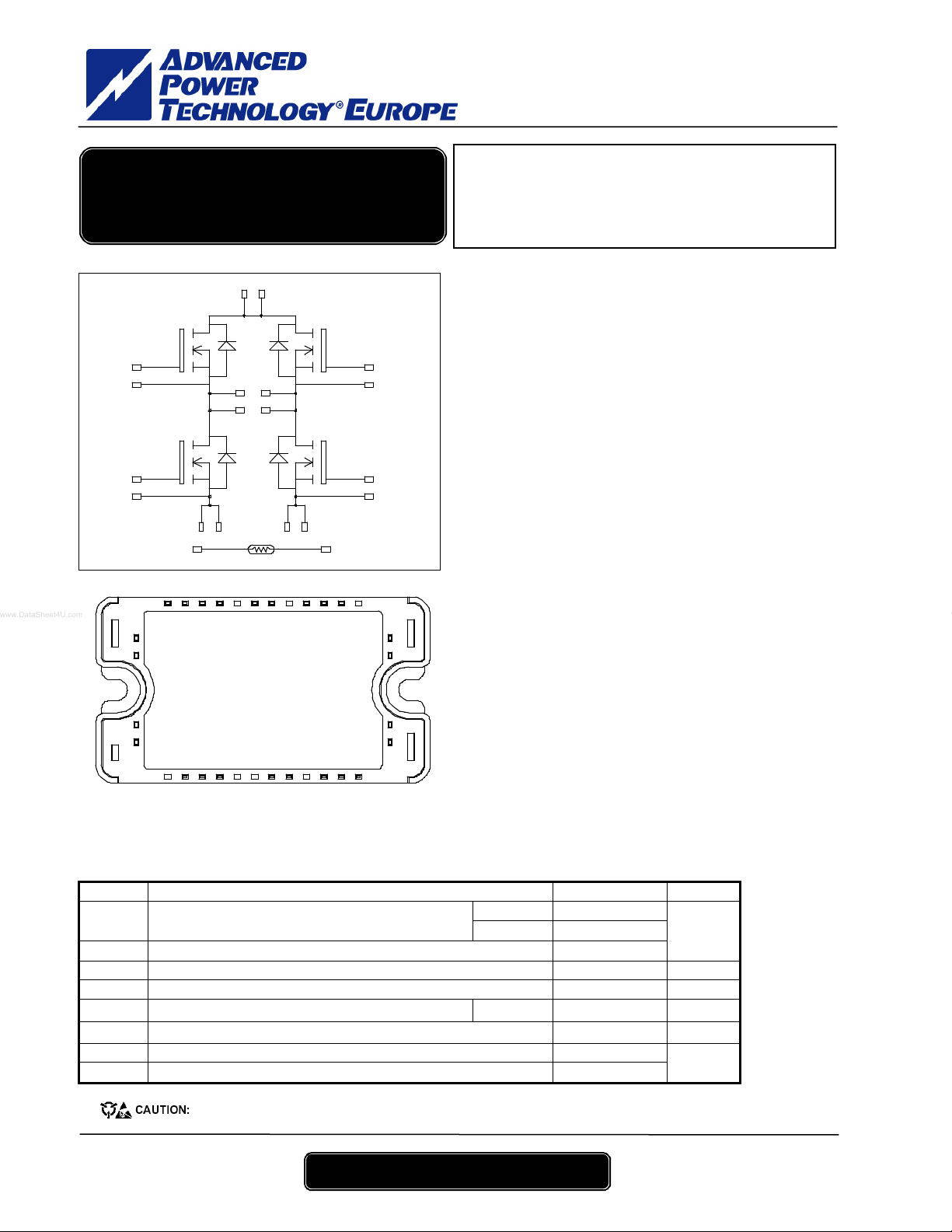
All multiple inputs and outputs must be shorted together
ull - Bridge
1413
Q1 Q3
11
7
22
10
23
Q2
29
15
28 27 26
2254
3
8
30
Example: 13/14 ; 29/30 ; 22/23 …
Q4
32
31
R1
87
16
182023 22
19
11
10
12
4
3
16
15
14
13
Absolute maximum ratings
ymbol Parameter Max ratings Unit
V
Drain - Source Breakdown Voltage 500 V
DSS
ID Continuous Drain Current
IDM Pulsed Drain current 140
VGS Gate - Source Voltage ±30 V
R
Drain - Source ON Resistance 100
DSon
PD Maximum Power Dissipation Tc = 25°C 312 W
IAR Avalanche curre nt (repetitive and non repetitive) 41 A
EAR Repetitive Avalanche Energy 50
EAS Single Pulse Avalanche Energy 1600
These Devices are se nsitive to Electrostatic Discharge. Proper Handing Procedures Should Be Followed.
V
R
I
= 500V
DSS
DSon
= 37A @ Tc = 25°C
D
Application
• Welding converters
• Switched Mode Power Supplies
• Uninterruptible Power Supplies
Features
• Power MOS 7® FREDFETs
• Kelvin source for easy drive
• Very low stray inductance
• Internal thermistor for temperature monitoring
• High level of integration
Benefits
• Outsta ndi ng pe r fo r mance at hi gh freq ue nc y operation
• Direct mounting to heatsink (isolated package)
• Low junction to case thermal resistance
• Solderable terminals both for power and signal for
easy PCB mounting
• Low profile
• Each leg can be easily paralleled to achieve a phase
leg of twice the current capability
Tc = 25°C 37
Tc = 80°C 28
= 100mΩ max @ Tj = 25°C
- Low R
- Low input and Miller capacitance
- Low gate charge
- Fast intrinsic reverse diode
- Avalanche energy rated
- Very rugged
- Symme trical design
DSon
A
mΩ
mJ
APT website – http://www.advancedpower.com 1 - 6
APTM50H10FT3 – Rev 1 December, 2004

APTM50H10FT3
All ratings @ Tj = 25°C unless otherwise specified
Electrical Characteristics
Symbol Characteristic Test Conditions Min Typ Max Unit
I
Zero Gate Voltage Drain Current
DSS
R
Drain – Source on Resistance
DS(on)
V
Gate Threshold Voltage VGS = VDS, ID = 1mA 3 5 V
GS(th )
I
Gate – Source Leakage Current VGS = ±30 V, VDS = 0V ±100 nA
GS S
VGS = 0V
VDS = 500V
VGS = 10V, ID = 18.5A 100
Dynamic Characteristics
Symbol Characteristic Test Conditions Min Typ Max Unit
C
Input Capacitance 4367
is s
C
Output Capacitance 894
oss
C
Reverse Transfer Capacitance
rss
Qg Total gate Charge 96
Qgs Gate – Source Charge 24
Qgd Gate – Drain Charge
T
Tur n-on Delay Ti me 15
d(on)
T
Rise Time 21
r
T
Turn-off Delay Time 73
d(off)
T
Fall Time
f
Eon Tur n-o n Sw i tchi n g E nergy X 566
E
Turn-off Switching Energy Y
off
Eon Tur n-o n Sw i tchi n g E nergy X 931
E
Turn-off Switching Energy Y
off
VGS = 0V
VDS = 25V
f = 1MHz
VGS = 10V
V
= 250V
Bus
ID = 37A
Inductive switching @ 125°C
VGS = 15V
V
= 333V
Bus
ID = 37A
RG = 5Ω
Inductive switching @ 25°C
VGS = 15V, V
Bus
ID = 37A, RG = 5Ω
Inductive switching @ 125°C
VGS = 15V, V
Bus
ID = 37A, RG = 5Ω
Source - Drain diode ratings and characteristics
Symbol Characteristic Test Conditions Min Typ Max Unit
Continuous Source c ur r e nt
IS
(Body diode)
VSD Diode Forward Voltage VGS = 0V, IS = - 37A 1.3 V
dv/dt Peak Diode Recovery Z 15 V/ns
trr Reverse Recovery Time
Qrr Reverse Recovery Charge
X Eon includes diode reverse recovery.
Y In accordance with JEDEC standard JESD24-1.
Z dv/dt numbers reflect the li mitations of the circuit rather than the device itself.
IS ≤ - 37A di/dt ≤ 100A/µs VR ≤ V
IS = - 37A
VR = 250V
diS/dt = 100A/µs
Tj ≤ 150°C
DSS
Tj = 25°C 100
Tj = 125°C 500
61
49
52
= 333V
= 333V
545
635
Tc = 25°C 37
Tc = 80°C
28
Tj = 25°C 280
Tj = 125°C 600
Tj = 25°C 2.3
Tj = 125°C 6.4
µA
mΩ
pF
nC
ns
µJ
µJ
A
ns
µC
APT website – http://www.advancedpower.com 2 - 6
APTM50H10FT3 – Rev 1 December, 2004
 Loading...