APSemi APS1026
)
Dual Channel 1.5 MHz, 600mA
Synchronous Step-Down DC-DC Converter
GENERAL DESCRIPTION
APS1026 is a dual channel high efficiency
monolithic synchronous step down current mode
DC-DC converter operating at 1.5MHz constant
frequency. The device integrates a main switch
and a synchronous rectifier for high efficiency
without an external Schottky diode for each of
the channels. The APS1026 can operate from a
2.5V to 5.5V input voltage and is ideal for
powering portable equipment that runs from a
single cell lithium-Ion (Li+) battery. It can supply
600mA output current for each channel and can
also run at 100% duty cycle for low dropout
operation, extending battery life in portable
system.
User can select between idle mode or power
saving mode via Mode/Sync input pin. Idle
mode provides low ripple noise at light load
while power saving Mode provides high
efficiency at light load.
APPLICATIONS
• Portable Media Players
• Digital Still Cameras
• Cellular Telephones
• PDAs
• Wireless and DSL modems
FEATURES
• High Efficiency: Up to 95%
• 600mA Output Current at Vin=3.0V
• 1.5MHz Constant Frequency Operation
• Very Low Quiescent Current of 40uA
• No Schottky Diode Required
• Low R
Internal Switches: 0.35Ω
DS(on)
• 0.6V reference allows low Output Voltage
• Current Mode Operation for excellent line
and load transient Response
• Short-Circuit & Thermal Fault Protection
• <1μA Shut Down Current
• Power-On Reset Output
• Externally Synchronizable Oscillator
• Small Thermally Enhanced MSOP-10 and
DFN-10 Package
EVALUATION BOARD
Board Number Dimensions (Inches)
EV1026EMJ
(MSOP)
EV1026EDJ
(DFN)
2.4”X x 2.4”Y x 0.5”X
2.4”X x 2.4”Y x 0.5”X
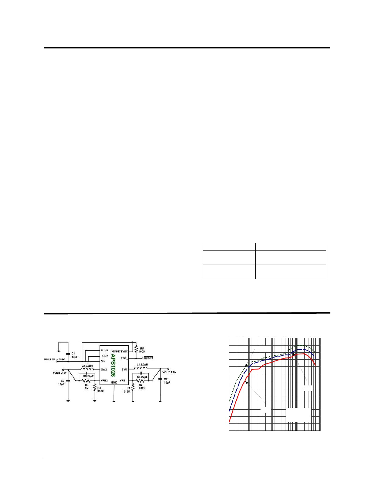
Typical Application
Figure 1. Basic Application Circuit
.
Analog Power Semiconductor Version_1.0 1/25/2006 1
APS1026 Efficiency vs Load Current
100
95
90
85
80
75
70
65
60
EFFICIENCY ( %)
55
50
45
40
35
0.1 1 10 100 1000
1.8V
1.2V
LOAD CURRENT (mA
TA = 25C
V
= 3.3V
IN
1.5V
APSemi APS1026
+0.3V
IN
(Note 1)
Peak SW1, SW2 Sink & Source Current ..... 1.5A
Operating Temperature Range... -40°C to +85°C
Junction Temperature
(Note2)
.....................+125°C
Storage Temperature Range .... -65°C to +150°C
Lead Temperature (Soldering, 10s).........+300°C
Absolute Maximum Rating
Input Supply Voltage ...................... -0.3V to +6V
RUN1, RUN2........................... -0.3V to VIN+0.3V
VFB1, VFB2 Voltages ............. -0.3V to VIN+0.3V
SW1, SW2 Voltages................ -0.3V to V
POR Voltages ......................... -0.3V to VIN+0.3V
Package/Order Information
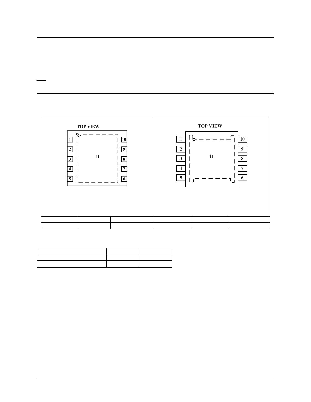
10-Lead (3mm X 3mm) Plastic DFN
Exposed Pad is PGND (Pin 11)
Must be connected to GND.
10-Lead Plastic MSOP
Exposed Pad is PGND (Pin 11)
Must be connected to GND.
Part Number Top Mark Temp Range Part Number Top Mark Temp Range
APS1026EDJ D2XY
(Note4)
-45℃ to 85℃
APS1026EMJ D1XY
Thermal Resistance
Package Ө
MSOP-10 (EXPOSE PAD)
DFN-10 (EXPOSE PAD)
Note 1: Absolute Maximum Ratings are those values beyond which the life of a device may be impaired.
Note 2: TJ is calculated from the ambient temperature T
T
Note 3: Thermal Resistance is specified with approximately 1 square of 1 oz copper.
Note 4: XY = Manufacturing Date Code. X = Year and Y = Week.
= TA + (PD) x Ө
J
JA
.
(Note 3)
:
JA
Ө
JC
45℃/W 10℃/W
45℃/W 10℃/W
and power dissipation PD according to the following formula:
A
-45℃ to 85℃
Analog Power Semiconductor Version_1.0 1/25/2006 2
APSemi APS1026
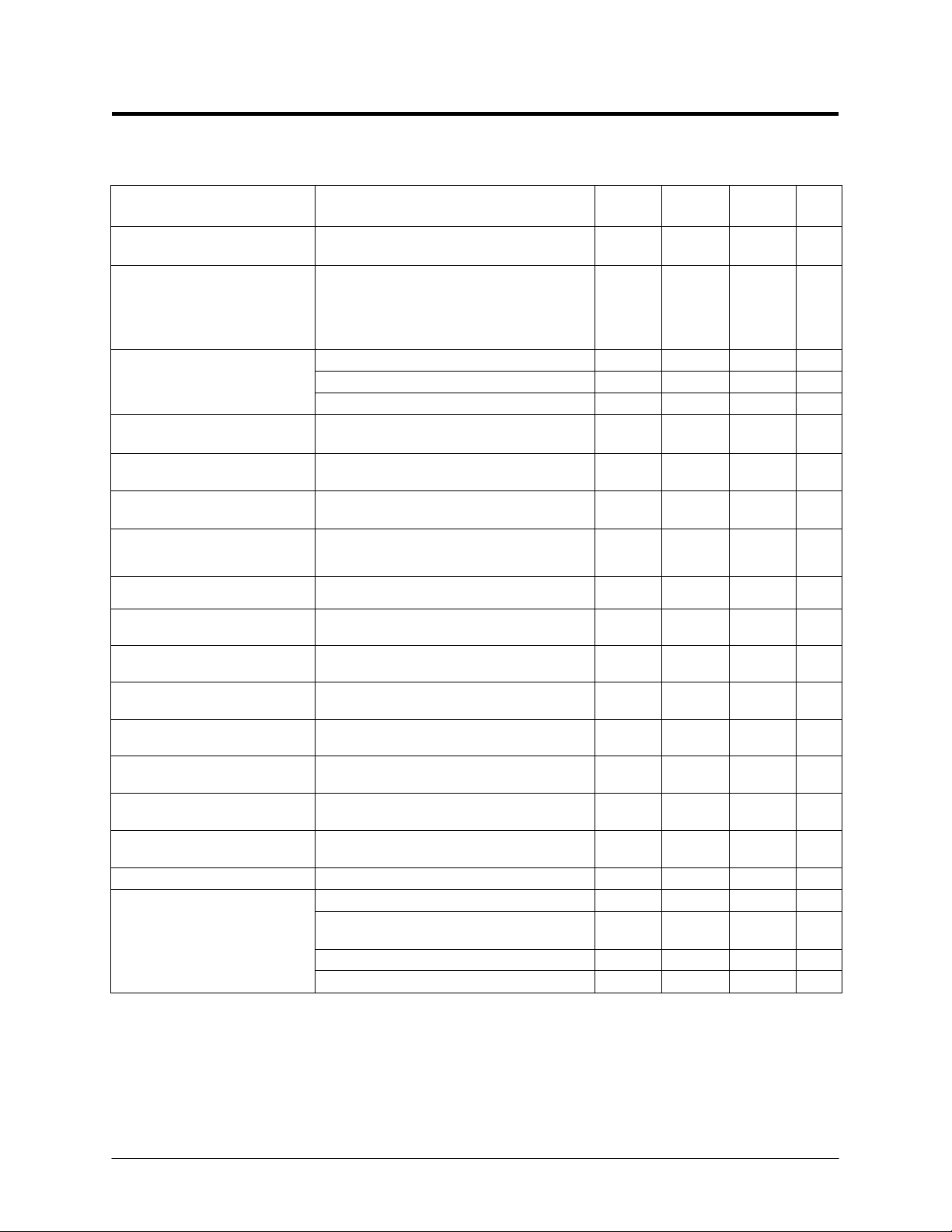
Electrical Characteristics
(VIN =V
= 3.6V, TA = 25°C, Test circuit of Figure 3, unless otherwise noted.)
RUN
(Note 5)
Parameter Conditions MIN TYP MAX Unit
Input Voltage Range 2.5 5.5 V
Input DC Supply Current
Active Mode
Sleep Mode
Shutdown Mode
Regulated
Feedback Voltage
V
= V
= V
= 0.5V, MODE = GND
FB2
= 0.63V, MODE = 3.6V
FB2
FB1
V
FB1
RUN = 0V, VIN = 4.2V, MODE = 0V
500
45
0.3
TA = +25°C, Channel 1 or 2 0.5880 0.6000 0.6120 V
TA= 0°C TA 85°C, Channel 1 or 2 0.5865 0.6000 0.6135 V
T
= -40°C TA 85°C, Channel 1 or 2 0.5850 0.6000 0.6150 V
A
800
60
2
µA
µA
µA
Feedback Pin Input Current VFB = 0.65V ±30 nA
Reference Voltage Line
Regulation
Output Voltage Line
Regulation
Output Voltage Load
Regulation
= 2.5V to 5.5V, V
V
IN
VIN = 2.5V to 5.5V, V
I
= 10mA
OUT
= VFB (R2=0) 0.04 0.40 %/V
OUT
= 1.8V,
OUT
VIN = 3.6V, ,
I
= 0 to 600mA, Mode = 3.6V or 0V
OUT
0.24 0.40 %/V
0.0015 %/mA
Maximum Output Current V
Oscillator Frequency V
R
R
of P-CH MOSFET VIN = 3.6V, IL = 100mA 0.35 0.45
DS(ON)
of N-CH MOSFET VIN = 3.6V, IL = 100mA 0.28 0.45
DS(ON)
Peak Inductor Current VIN=3V, V
SW Leakage V
Output Over Voltage
Lockout
= 3.0V 600 mA
IN
= 0.6V 1.2 1.5 1.8 MHz
FB1/2
= V
FB1
= 0V, VSW= 0V or 5V, VIN = 5V ±0.01 ±1 µA
RUN
V
OVLX
= V
OVLX
= 0V, SW1 or SW2 1.0 A
FB2
– V
20 50 80 mV
FBX
RUN Threshold -40°C TA 85°C 0.3 0.45 1.30 V
RUN Leakage Current ±0.1 ±1 µA
V
Ramping Up, MODE/SYN = 0V 8.5 %
FBX
V
Ramping Down, MODE/SYN =
Power-On Reset Threshold
(POR)
FBX
0V
Power-On Reset Delay 175 mS
-8.5 %
Power-On Reset On-Resistance 100
Note 5: 100% production test at +25°C. Specifications over the temperature range are guaranteed by design and
characterization.
Analog Power Semiconductor Version_1.0 1/25/2006 3
APSemi APS1026
)
)
)
)
)
)
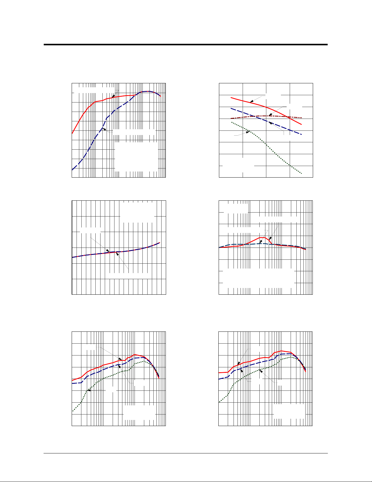
Typical Performance Characteristics
(Test Figure 1 above unless otherwise specified)
Efficiency vs Load Current
100
Power Saving Mode
90
80
70
60
50
40
EFFICIENCY (%)
30
20
10
0
0.1 1 10 100 1000
Oscillator Frequency vs Supply Voltage
1.8
1.7
Idle Mode
1.6
Pulse Skipping Mode
VIN = 3.6V
VOUT = 1.8V
TA = 25C
NO LOAD ON
OTHER CHANNEL
LOAD CURRENT (mA
L = 2.2μH
Iload = 150mA
Vout = 1.8V
Efficiency vs Input Voltage
100
95
90
85
80
1mA
75
EFFICIENCY (%)
70
TA = 25C
65
VOUT = 1.8V
60
2 3 4 56
4.0
TA = 25C
3.0
2.0
Pulse Skipping Mode
1.0
100mA
10mA
INPUT VOLT AGE (V
Load Regulation
Power Saving Mode
600mA
1.5
1.4
OSCILLATOR FREQUENCY (MHz)
1.3
1.2
2.7 3.15 3.6 4.05 4.5 4.95 5.4
Power Saving Mode
SUPPLY VOLTAGE (V
Power Saving Mode Operation
Efficiency vs Load Current
100
95
90
85
80
75
EFFICIENCY (%)
70
65
2.7V
3.3V
4.2V
TA = 25C
VOUT = 1.2V
0.0
ERROR (%)
OUT
-1.0
V
-2.0
VIN = 3.6V
VOUT = 1.8V
-3.0
NO LOAD ON OTHER CHANNEL
-4.0
1 10 100 1000
LOAD CURRENT (mA
Power Saving Mode Operation
Efficiency vs Load Current
100
95
90
85
80
75
EFFICIENCY (%)
70
65
2.7V
3.3V
4.2V
TA = 25C
VOUT = 1.5V
60
1 10 100 1000
LOAD CURRENT (mA
Note: No load on the other channel
60
1 10 100 1000
LOAD CURRENT (mA
Note: No load on the other channel
Analog Power Semiconductor Version_1.0 1/25/2006 4
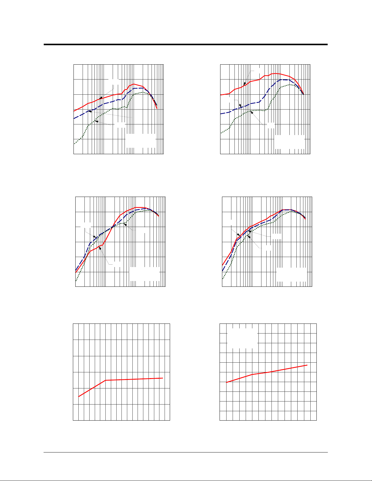
APSemi APS1026
)
)
)
)
)
)
Power Saving Mode Operation
Efficiency vs Load Current
100
95
2.7V
Power Saving Mode Operation
Efficiency vs Load Current
100
2.7V
95
90
85
EFFICIENCY
80
75
70
1 10 100 1000
LOAD CURRENT (mA
4.2V
3.3V
TA = 25C
VOUT = 1.8V
Note: No load on the other channel
Idle Mode Operation
Efficiency vs Load Current
100%
90%
3.3V
80%
70%
EFFICIENCY (%)
60%
2.7V
50%
40%
1 10 100 1000
LOAD CURRENT (mA
4.2V
TA = 25C
VOUT = 1.8V
Note: No load on the other channel
Oscillator Frequency vs Temperature
1.800
1.700
1.600
1.500
1.400
FREQUENCY (MHz)
1.300
1.200
-48 -32 -16 0 16 32 48 64 80 96
TEMPERATURE (C
90
3.3V
85
EFFICIENCY (%)
80
75
70
1 10 100 1000
LOAD CURRENT (mA
4.2
TA = 25C
VOUT = 2.5V
Note: No load on the other channel
Idle Mode Operation
Efficiency vs Load Current
100%
90%
2.7V
80%
4.2V
3.3V
TA = 25C
VOUT = 1.5V
70%
EFFICIENCY (%)
60%
50%
40%
1 10 100 1000
LOAD CURRENT (mA
Note: No load on the other channel
VFB vs Temperature
0.612
0.610
0.608
0.605
0.602
0.600
0.598
VOLTAGE (C)
0.595
0.592
0.590
0.588
Vin = 3.6V
Vout = 1.8V
Iload = 0mA
-50 -30 -10 10 30 50 70 90
TEMPERATURE (C
Analog Power Semiconductor Version_1.0 1/25/2006 5
 Loading...