


APLUS INTEGRATED CIRCUITS INC
DevicePlayback ice Recording & oVle-Chip Sing
nd MessageSecoto 30 for Single 20
sureFeat
kbacay & plingrdo rececioty vli quagh, hiiphe-cngliS•
onitluso
ed irequ r ICsnalrtexo eN-
ntsoneomp cnalter exumimniM -
ygolnoche tyr mo mehsal Feliatolv-on N•
ed irequ r upck bayrtteao bN-
)laciyp (tse ycl c rdco reK001-
)alic ypt (iontente ragesmes reay-100-
or tsi reslrnaetxe thi w,sdcon se to 300e of 2agssee mngliS •
noitclese
hesct swikbacaypl
ntioumpns coer powLow•
lyuppr s e V powe 65ngliS •
noatipere ouso-t-sy, ealyendirf-resU•
t: 1uA (typical, no load)enrrby cuandtS-
.
ed irequt r noemsst syent opmeldev & ingammrgorP-
ted vatiacge- edng &idroce rdateivtca-elLev-
ad) loo, nalicpyt ( mA5t: 2enrr cugnatiperO -
elifry tteaer bongfor lure featn owr-d ewo pcatiom tuA•
onsipan exagessele mmp si forpinle nabp ehiC •
noiiptscrl DeneraeG
etstad- ilop si-chlegniue srrs tfe fce ovi dee APR9301 Th
errollontocrci mr oareftwsono sire ureqnd atyibilpacage ora ts
thi wkcaby plaandng rdi orecty lia-qughi hsideovr It port.upps
etablr porl foa ide istge. Iassend moc-se 30ot 20-elg sina
der anumonscr heto nyd ma, ans toy,ersrdoe recciov
s.onicat li appalstrindui
si gyloonhe tecorag st leveti-lul/mgalo anAPLUS integrated
,llsry cemo meetillaon-vh noaslF edanc advni tedenem lpmi
eltag6 voan 25re thoore my stllacin typh caich wfo chae
eicos vceodu repr andesr sto -V2 APR9301. Thelsevel
istah t onitortsie dh g t nitainiml e,smrol farut na rieh t inslagnsi
eic dev Theon. isrespmod c angnicod end byceodur intfteno
n- no, ionptumonsr cew pow lohti wzei sallsm a esinbmoc
ecivo ot noitlue soivtce effst a corof esu-f-oesae d, anytliitlavo
.ckbayalnd pg ardincore
.
1ageP
g
g
g
g
y
g
g
g
y
g
y
(edg
y
g
y
y
g
y
y
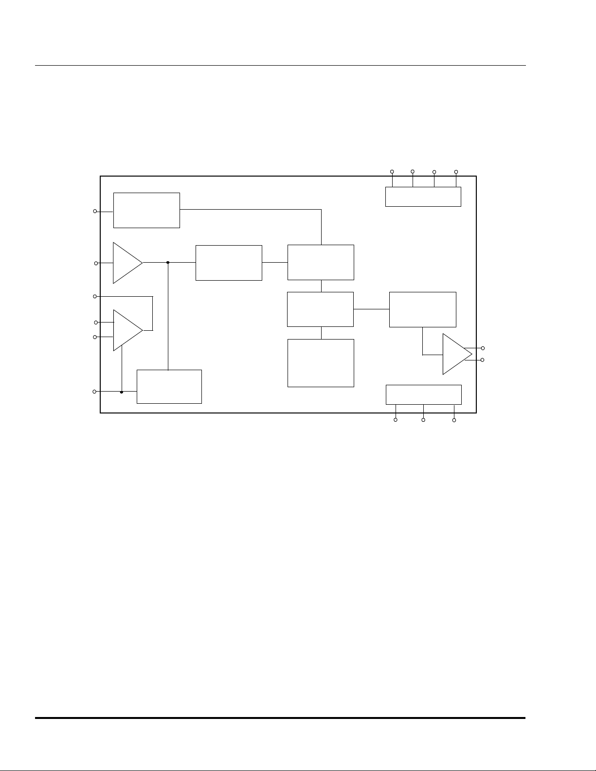
APLUS APR9301-V2
Functional Block Diagram
Figure 2 shows the functional block diagram for the APR9301-V2
Figure 2 APR9301 -V2 Functional Block Diagram
V
V
V
CCA
CCD
SSD
V
SSA
OscR
AnaIn
AnaOut
MicIn
MicRef
Internal
Oscillator
Amp
Pre-
Amp
Switched
Capacitor Filter
Automatic G ain
AGC
Control (AGC)
Sample Application
Figure 3 shows the diagram for a single, 20-second message
recordin
device. When pins are connected as shown in this example,
the operating modes are as follows:
Record Mode (Level-Activated)
A sin
The /LED pin will
to provide a visual indication if an LED li
this pin. The chip is in record mode as long as the /RecL pin
sta
20 seconds, recordin
last available memory cell is written. If the message is shorter
than 20 seconds, the recordin
the /RecL pin
tristated during the recording operation.
Messages of up to 30 seconds can be recorded by usin
different OscR resistor values (see Table 1).
and playback application using theAPR9301
le voice message of up to 20 seconds can be recorded.
o low during the actual recording process
ht is connected to
s low (level-activated). If the message lasts longer than
will terminate automatically after the
operation will stop when the
oes high. The speaker driver is automaticall
Power Supplies
Sample & Hold
Circuit
Analog W rite &
Read Circuits
Non-Volatile
Analog Storage
Mem ory Array
Playback Mode (Edge-Activated)
Playback always starts from the beginning of the message.
The chip is in pla
e-activated). Playback will stop immediately when the
E pin pulses low a second time. If the newly recorded
/Pla
messa
the remaining portion of the previous message will not be
pla
amplifier, AGC, and main amplifier circuits are disabled
during playback.
Standby Mode (/CE = "0")
The chip will automaticall
recordin
Power Down Mode (/CE = "1")
The chip is alwa
is allowed. Current consumption is t
e is shorter than the previously recorded message,
ed after the new message is played back. The input pre-
or playback operation is completed.
back mode after the /PlayE pin pulses low
s in standby state. No recording or playback
Switched
Capacitor Filter
Amp
Device Control
/PlayE
/RecL
return to the standby state after
/LED
pically less than 1 uA.
SP+
SP-
Pag
e 2

APLUS APR9301-V2
Figure 3 Sample Application for the APR9301-V2
VCC(6VDC)
For low power applications
use double pole switch.
VCC
220K
1K
4.7K
Electret
Microphone
150K
4.7µF
22
µ
F
52K
NC
NC
NC
NC
NC
/CE
OscR
NC
NC
NC
NU1
V
SS
SP+
SP-
V
1
2
3
4
5
6
7
8
9
10
11
12
13
14
8 Ohm Speaker
28
27
26
25
24
23
22
21
20
19
18
17
16
15
CCD
/RecL
V
SSD
/LED
NC
/PlayE
NC
AnaOut
AnaIn
AGC
MicRef
MicIn
VccA_R
VccA_L
0.1uF
0.1µF
VCC
0.1
VCC
µ
F
1K
47u
Notes:
NC = No Connect (must be floating).
Pins 23 and 27 have internal pull-up resistors.
The typical sampling frequency is 6.4 kHz with OscR = 52 k
0.1µF
W. Substrate should be connected to GND.
4.7K
Table 1 Typical Dependence of Sampling Frequency and Total Voice Duration on OscR Resistor Value
= V
(V
CCA
Pin 7 - OscR Typical Sampling Frequency Cutoff Frequency (3 dB Point) Typical Total Voice Duration
W
38 k
W
52 k
W
67 k
W
89 k
CCD
= 6V; V
SSA
= V
= 0V; TA = 25oC)
SSD
8 kHz 3.4 kHz 16 seconds
6.4 kHz 2.7 kHz 20 seconds
5.3 kHz 2.3 kHz 24 seconds
4.0 kHz 1.7 kHz 32 seconds
Page 3
 Loading...