

Page 1

DOMINATOR
II
PRECISION
PEAK LIMITER
OPERATING GUIDE
MUL
TIBAND
APHEX
11068
Randall
SYSTEMS,
Street,
Sun
L
TO.
Valley,
CA
91352
(818)
767-2929
Page 2

DOMINATOR
1-1
II
PRECISION
1.0
After
world
effectiveness.
reputation,
techniq
As a
same
INTRODUCTION
its
introduction
standard
ues.
direct
primary
for
peak
However,
Aphex
The
descendant
functions
Systems.
result
MUL TIBAND PEAK LIMITER
in
1985,
limiting
un
is
of
and
the
because
willing
Ltd,
the
the
applications.
has
Dominator
original.
Studio
to
rest
continued
Dominator
of
its
on
its
II.
the
Dominator II
Its
many
became
transparency
already
to
develop
performance
the
and
established
new
has
the
improvements
flexibility,
Although
much
these
manual.
The
Dominator
zero
higher
and
the
audio
those
of
the
people
overshoot.
amplitude
price
application,
lie
in
and
ease
familiar
information
as
well
II
is a stereo
Once
in
of
exceeding
is
the
areas
of
setup.
with
in
as
those
the
the
output.
critical
of
the
this
manual,
new
multiband
PEAK
those
for
dynamic
Studio
to
Aphex
peak
CEILING
Awareness
limitations,
most,
especially
range,
Dominator
Aphex
is
recommends
Dominators
limiter
set,
of
headroom
important
distortion,
already
read
with
there
digital.
is
for
know
that
this
a,bsolute
no
limitations
any
The
Dominator
quickly
by
II
allows
freeing
users
them
to
from
work
the
confidently.
fear
of
"crashingll.
creatively,
and
Page 3

1-2
Achieving
is
the
exceptional
many
•
BROADCASTING-PRODUCTION.
FM. AND
.
RECORDING
•SAMPLING
.MIXING
•
MASTERING-CD.
· SOUND REINFORCEMENT
· SATELLITE AND
.LOCATION
· VIDEO
·
TAPE
this
art
and
science
function
audio
fields.
TV
POST-PRODUCTION
DUPLICATION
brick
wall
of
and
including:
FILM. AND ANALOG
STL
RECORDING
result
the
while
Dominator
performance.
UPLINK
retaining
II.
it
has
AND
complete
Because
of
applications
TRANSMISSION
DISK
fidelity
its
in a great
FOR AM.
•
TELECONFERENCING
1.1 DYNAMIC RANGE CONTROL
Essential
the
Dominator
for
each
to a full
II
type
of
understanding
is a knowledge
gain
control:
leveling,
clipping.
1.1.1
Leveling
Leveling
times.
effect
has
Because
on
short
high
term
compression
of
its
very
changes
ratios
slow
in
of
the
of
the
with
time
average
operation
definitions
compre~sion,
slow
constants.
levels
and
and
attack
leveling
or
on
application
applications
limiting.
and
release
has
transient
of
and
no
peaks.
Therefore.
affecting
in
the
input
level
signals
the
it
is
short
signal.
will
used
term
be
to
maintain a constapt
dynamics
Typically,
brought
the
up.
by
adjusting
threshold
output
for
is
set
level
long
low
without
term
so
that
changes
low
Page 4

1-3
1.1. 2
Compression
Compression
compressor
size
of
the
the
threshold,
attack
constan
actual
used
and
ts,
quality
creatively.
compression
low.
1.1.
3
Limitin
has
forces
resulting
the
release.
the
greater
and
is
to
g
low
ratios
a
wide
dynamic
height
The
the
fidelity
Normally,
bring
with
dynamic
of
higher
effect
of
since
up
low
range
the
the
level
faster
range
depends
ratio
the
ratio
on
the
sound);
one
signals.
attack
and
into a smaller
on
used.
and
short
and
the
term
these
of
the
desired
the
release
the
level
the
faster
dynamics
effects
results
threshold
range.
speed
are
times.
of
of
the
often
is
A
The
the
time
(the
of
set
Limiting
8:
1),
fast
desired
to
keep
the
ratios
dynamic
or
may
the
average
the
limiter
attack
a
peak
1.1. 4
Clipping
has
attack
sound,
high
are
range
not
is
times
limiter.
high
and.
slow
levels
high.
of
be
desirable.
level.
considered
is
increased
compression
depending
or
fast
down.
as
the
the
the
output
If
and
allow
a
to
ratios
release
threshold
input
becomes
the
for
peaks
program
control
on
the
times.
is
driven
attack
limiter.
peaks.
(usually
particular
is
'tighter',
times
above
defined
Since
set
high.
further
are
the
When
the
limiter
application
it
into
an
effect
set
threshold
the
as
is
normally
Inasmuch
limiting,
to
control
speed
is
greater
and
used
as
that
may
only
to
pass,
of
the
considered
than
the
Regardless
time
before
of a limiter's
the
detector
attack
circuits
time.
cause
there
the
is a finite
gain
circuits
amount
to
of
reduce
Page 5

the
output
below
threshold.
Also,
extremely
fast
gain
1-4
modulation
introduces
infinite
absolute
off
the
amplitude
is
inaudible
audio.
obnoxious
unwanted
ratios
brick
peaks
of
Done
effects.
and
instantaneous
wall.
of
the
the
remainder
and,
under
improperly,
audible
To
control
wave
certain
effects.
attack
the
above
of
threshold
the
circumstances,
however,
peaks,
wave.
clipping
Therefore,
and
release,
clipping
without
Done
produces
clipping
functions
literally
changing
properly,
actually
with
clipping
enhances
very
audible,
its
as
shaves
the
an
the
Page 6
2-1
2.0
Traditionally,
times:
above
is
short
density
attack
cause
the
combining
FUNCTIONAL
the
threshold.
that
the
ones.
(peak
times
distortion,
overshoots
peak
faster
limiter
The
to
result
..
limiters
limiters
the
attack
The
is
triggered
sonic
average
in
better
or
the
The
Dominator
with
DESCRIPTION
have
drawback
result
ratio).
overall
fairly
time,
off
is
sonic
slow
been
to
hole
level
II
designed
the
lower
these
each
punching
On
the
performance,
must
overcomes
attack
the
fast
attack
transient,
other
be
reduced
both
times
with
amount
even
and
hand,
the
drawbacks
and
fast
attack
of
overshoot
times,
extremely
overall
while
overshoots
to
accommodate
clipping,
however,
lower
slower
by
in
an
interactive,
The
Dominator
adjustable
users
peaks
set
2.1
A
intermodulation"
con
being
have
must
it
and
MULTI BAND
significant
troIs
'sucked
self-adjusting
threshold.
only
stop
forget
the
level
II
has
to
set
(for
it!
VERSUS
problem
which
of
down'
manner.
been
example:
with
another
whenever
designed
Since
the
PEAK
WIDE BAND
wideband
occurs
there
100%
when
part.
the
as a unity
is
zero
CEILING
modulation).
PROCESSING
processing
one
part
A
typical situa
kick
drum
gain
overshoot
to
the
is
of
the
hits.
device
over
level
In
at
other
"spectral
spectrum
tion
is a vocalist
with
an
threshold,
which
words.
gain
Page 7
2-2
Since
to
are
causing
Multiband
into
separately.
to
While
for
Since
most
control
above
the
two
control,
this
almost
the
energy
the
level
the
limit
output
processing
or
more
However,
including
creates
every
Dominator
is
contained
of
the
threshold,
to
be
solves
frequency
more
a
method
user
different
flexibility,
II
uses
entire
dull.
these
bands,
bands
source.
program
in
the
spectrum.
higher
problems
often
of
summing
it
lower
frequencies
and
processing
result
also
requires
dependent,
frequencies,
When
are
by
splitting
in
the
bands
intelligent
lower
attenuated,
the
each
many
different
more
together
they
frequencies
band
tend
audio
parameters
again.
settings
circuits
that
reduce
shape
effective
2.2
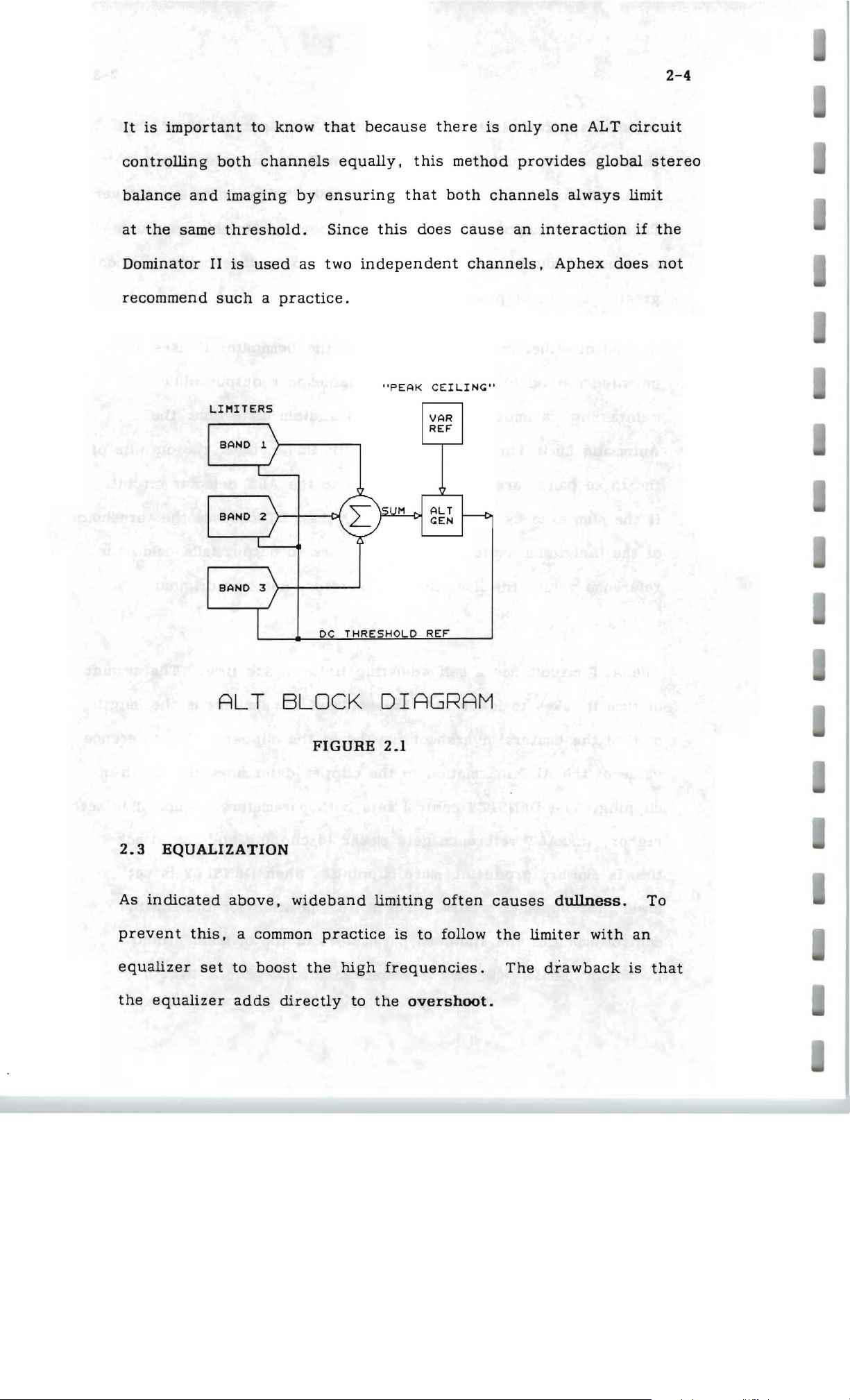
[Reference:
processor
individually,
each
produces
One
the
limiting.
ALT
band's
an
conventional
the
number
sound
(AUTOMATIC
splits
while
Fig.
peak
unpredictable
and
2.1
ALT
the
audio
then
output
approach
of
controls,
quickly
LIMIT
sums
is
and
easily
THRESHOLD)
BLOCK DIAGRAM,
into
separate
the
bands
predictable,
peak
to
output.
making
users
bands,
together
summing
the
have
achieving
Page
limits
again.
summed
the
flexibility
consistent,
2-4].
the
output
A
each
Even
bands
predictable
to
multiband
band
though
together
is
to
use
introduces
a wide
all
the
band
limiter
drawbacks
after
of
wideband
the
summing.
limiting
Unfortunately,
identified
above.
this
Page 8
2-3
Another
this
high.
far
approach
causes
To
below
is a loss
greater
Instead
amount
of
patented
maintaining
Automatic
the
three
If
the
sum
too
avoid
the
clipper
of
loudness
either
method
maximum
Limit
bands
exceeds
is
to
much
this
clipping
distortion,
threshold.
and,
of
processing.
of
these
to
produce
loudness
Threshold
are
summed
a
reference
use a clipper
distortion
the
The
because
approaches,
a
predictable
without
(AL
T).
and'
sent
value,
on
limiters'
drawback
of
the
the
audible
Wfth
to
the
the
summed
if
the
summed
thresholds
lower
thresholds,
Dominator
peak
output
distortion:
this
method,
the
AL T detector
AL T reduces
to
output,
this
II
the
output
are
approach
a
uses
while
the
outputs
circuit.
the
thresholds
but
is
set
much
a
too
very
of
of
the
reference
setting.
The
ALT
of
time
of
time
value
of
clipping.
higher,
time
is
lower,
control
individual
value,
circuit
it
takes
the
limiters'
the
AL T in
The
DENSITY
the
AL T reference
slower,
the
opposite
emulates
limiters.
the
limit
When
thresholds
has a self-adjusting
to
lower
the
overshoot
relation
thresholds
may
to
control
gets
producing
occurs.
the
standard
more
The 0 RCH
parameters
the
summed
return
finite
be
the
clipper
sets
both
closer
clipping.
attack
of
the
in
the
determines
parameters.
to
clipping
When
position
of
output
to
their
limiters
clipper.
DENSITY
the
original
time.
and
for
falls
below
original
The
is
the
The
the
When
the
is
the
DENSITY
Studio
the
amount
length
reference
depth
it
is
attack
set
of
set
Dominator.
Model 700;
this
is
recommended
for
general
use.
Page 9
It
is
important
to
know
that
because
there
is
only
one
ALT
2-4
circuit
controlling
balance
at
the
and
same
Dominator
recommend
both
channels
imaging
by
threshold.
II
is
used
as
such a practice.
LIMITERS
BAND 1 )-------,
BAND
2
)--+--C>!
equally,
ensuring
Since
two
this
independent
that
"PEAK
MALT
this
both
does
CEILING"
VAR
REF"
GEN
method
channels
cause
channels,
provides
an
interaction
Aphex
global
always
limit
if
does
stereo
the
not
2.3
As
EQUALIZATION
indicated
prevent this,
equalizer
set
BAND
3
ALT
above,
a common
to
boost
DC
THRESHO REF
BLOCK
FIGURE
wideband
practice
the
high
DIAGRAM
2.1
limiting
is
frequencies.
to
often
follow
causes
the
limiter
The
dullness.
with
drawback
an
is
To
that
the
equalizer
adds
directly
to
the
overshoot.
Page 10

2-5
Another
detector
the
practice
circuits.
drawback
frequencies,
The
Dominator
processing
mid-band
to
the
low
so
that
when
threshold,
means
in
that
below
threshold
with
and
and
the
the
is
is
that
it
creates
II
eliminates
selectable
between
high-band.
the
EQ
Dominator
Dominator
audio
to
attenuate
While
this
when
unacceptable
mid
controls
performance,
diminishes
there
these
crossover
and
high-band,
Also,
are
II will
II
equals
the
lower
is
substantial
amounts
problems
frequencies
the
set
pass
perfect
a well
frequencies
spectral
by
with
crossover
flat
and
designed
and
vastly
gain
energy
of
overshoot.
using
between
adjustable
filters
the
square
outperforms
fed
to
intermodulation,
in
those
three-band
low
input
are
designed
input
is
below
waves.
wideband
the
lower
and
levels
This
limiter
any
wideband
The
selection
each
When
band
the
response
compression
the
input
output
and
2.4
level.
still
maintain
RELEASE
device
helps
input
equal
ratio
level
in
of
the
determine
is
below
to
the
of
above
The
an
TIME
performing
crossover
the
the
change
the
limiter
threshold
EQ
provides
absolute
its
function
frequencies
frequency
limit
threshold,
in
input
is
essentially
will
user
peak
ceiling.
response
in
each
not
cause
flexibility
above
and
the
infinite,
any
threshold.
the
of
EQ
band.
change
to
shape
input
the
will
Since
a
level
output.
give
the
change
in
the
sound
to
a
in
the
The
With
close
release
faster
as
possible
time
release
allows
times,
to
maximum.
users
the
to
adjust
output
Extremely
the
density
is
consistently
fast
release
of
the
output.
maintained
times
as
result
Page 11

2-6
in a very
distortion.
rounder,
output
much
inputs.
2.5
An
a
GAIN
important
signal
function.
more
than a straight
tight
Slower
softer
lower
CONTROL
design
processor
That
dynamic
release
sound.
in
average
CIRCUITS
goal
able
is,
it
must
wire--no
range,
times
Very
for
to
do
and
reduce
slow
amplitude,
all
Aphex
nothing
be
able
noise,
also
may
the
release
especially
products
before
to
pass
distortion,
cause
distortion
times
tend
has
it
performs
audio
as
or
low
and
to
on
transient
been
if
it
color.
frequency
provide
make
to
the
make
its
were
nothing
a
Essential
to
performance
specifications
importantly,
Others
audio
extreme
gain
control
produce
which
importance
is
changed
feedthrough
unintended
is
completely
situations
such
achieving
integrated
are
outstanding
its
dynamic
distortion
do
not
rapidly.
signal
free
fed
from
as a peak
that
gain
appear
is
that
whose
to
these
goal
is
the
control
as a signal
performance
or
amplitude
with
steady
other
The
sonic
the
devices
best
results
control
anomalies,
limiter.
use
element.
amplifier,
surpasses
anomalies
tone
also
known
include
circuits.
even
of
the
Its
all
test
measurements.
create
anomaly
clicks,
The
in
the
Aphex
measured
but
other
with
complex
anomalies
is
DC
pops,
Aphex
most
VCA
even
1001
more
devices.
program
when
shift
or
VCA
demanding
high
Of
or
1001
Each
preset
also
band
and
equal
has
equal
for
its
all
own
limiter
for
all
limiters.
and
limiters.
The
detector.
T
he
release
threshold
The
time
is
adjustable
attack
is
adjustable
time
from
is
and
the
Page 12

2-1
front
2.6
panel
TRACKING
Tracking
the
same
amount
have
an
stereo
loudness
stereo
limiting,
Peak
forces
band
of
limiting
equal
image.
can
be
imaging,
non-tracking
Ceiling
CONTROL
the
limiting
in
the
will
amount
Without
achieved
depending
control
other
cause
of
limiting.
the
may
of
channel.
the
tracking
but
with
on
the
be
preferred
and
each
same
This
amount
is
also
band
The
in
channel
band
control
control,
potentially
of
in
adjusted
each
in
the
maintains
increased
inaccurate
limiting.
many
channel
with
other
cases.
by
the
stereo
For
the
ALT.
to
follow
greatest
channel
a
stable
or
"smeared"
light
to
2.1
DENSITY
The
DENSITY
incorporated
the
DENSITY
effect,
(RCH)
this
cf
the
below-threshold
the
waveform
By
setting
essentially
duration
the
adjusts
of
clipping
control
in
to
control
allows
audio
peak
as
AL T
the
users
output
well
the
is
one
Dominator
adjusts
to
levels
as
greater
reference
average
allowed.
of
the
II.
the
parameters
determine
signal.
increase,
relative
level
depth
High
most
As
important
indicated
of
the
RELATIVE
With a higher
producing
loudness.
and
attack
of
clipping,
clipping
depth
improvements
in
section
the
AL T
CREST
RCH
greater
time,
this
and
and
circuit.
setting,
power
control
the
relative
duration
2.2
AL
In
HEIGHT
the
in
T,
create
clipping
work
low
to
distortion.
greater
depth
the
loudness,
and
limiters.
but
duration
Reduced
may
reduce
loudness
generate
clip
high
distortion,
and
'punch'
distortion.
transferring
is
traded
Low
more
for
Page 13
For
those
interested
in
the
technical
aspects,
when
the
2-8
DENSITY
control
below
are
at
the
the
thresholds
2.8
PEAK CEILING
Many
be
was
audio
as
high
designed
control
The
FINE
setting,
is
in
the
clipper
same
are
applications
as
with
switches
control
in
O.
2dB
12
o'clock
threshold.
level.
6dB
below
CONTROL
possible.
two
the
ceiling,
adjusts
steps.
position,
Fully
the
require
To
fulfill
controls
in
the
the
limiter
Fully
clockwise,
counterclockwise,
clipper.
that
the
peak
that
requirement,
for
the
output
2dB
ceiling
steps,
+1
to
from
-IdE
thresholds
the
limiter
the
limiter
output
ceiling.
+2
to
from
be
trimmed
the
The
+24dBu
the
are
3dB
thresholds
Dominator
COARSE
(peak).
COARSE
to
II
There
structure
output.
peak
The
maximum
adjusting
2.9
For
is a third
by
These
output
PEAK CEILING
peak
the
INPUT
maximum
transformerless
control,
adding
three
to
within
lOdB
controls
O.
controls
output).
PEAK CEILING
AND
audio
audio
OUTPUT
performance,
I/O
RANGE,
at
the
give
2dB
over a 34dB
set
If
the
controls
CIRCUITS,
circuits.
which
input,
the
input
the
adjusts
and
users
the
range.
threshold
level
does
BYPASS
Dominator
With
these,
the
subtracting
ability
of
remains
not
affect
RELAY
II
perfect
internal
lOdB
to
trim
clipping
below
threshold,
output
has
servo-balanced
interfacing
gain
at
the
(the
levels.
the
with
is
extremely
any
system.
simple.
balanced
or
unbalanced,
high
or
low
impedance,
Page 14
The
input
stage
and
AC
power
input
receptacle
include
2-9
radio
frequency
the
Dominator
The
servo
resistor
is
selected.
For
not
for
systems
select
19.5K-ohm.
The
servo-balanced
ohms
long
or
greater.
capacitive
filtering
II
balanced
systems
the
resistor
that
the
termination;
lines
to
to
be
input
which
don't
output
The
effectively.
reject
used
stage
need
is
lifted
require
unterminated,
stage
output
interference
in
typical
has a selectable
to
be
to
prevent
a
load
resistance,
properly
impedance
terminated
from
broadcast
loaded.
line
the
drives
of
65
or
transmitters
racks.
600
ohm
When
Bypass
loading
users
input
any
ohms
impedance
load
can
unterminated.
and
allow
termination
mode
disturbance.
simply
do
is
of
600
drive
The
especially
is
its
ability
difficulty.
is
GROUNDED
drive
full
A
automatically
output
high
Bypass
and
lifts
limiter
the
input
limiter
function
unique
to
For
level
quality
connects
the
input
stage
remains
can
be
characteristic
drive
balanced
unbalanced
to
pin
1.
to
the
(no
6dB
audio
the
relay
output
termination
is
still
active
initiated
and
output,
This
hot
pin
loss
as
provides
connector
resistor.
connected
for
instant
in
one
of
the
unbalanced
causes
only.
with
of
three
servo-balanced
the
unused
the
output
and
adjust
a
other
true
circuits).
hard-wired
directly
if
it
to
the
input
insertion
ways:
output
output
stage
to
the
was
selected.
connector;
in
line.
powering
output
gain
input
lines
pin
to
to
bypass
The
down
stage
without
(2
or
shift
all
provide
function.
connector
The
thus,
Bypass
or
3)
power
(rear
failure;
panel
front
jack).
panel
This
Process
Off/On
configuration
switch;
provides
or
a
fail-safe
remote
control
Page 15
2-10
characteristic
bypassed
power
2.10 MODEL
through
supply
Pre-emphasis
on
the
ratio
greater
technique
the
for
Primarily,
Starting
flat
for
critical
the
fails.
723
PRE
is
an
of a resistor
equalization.
broadcast
there
are
at
approximately
systems
Dominator
AND
DE-EMPHASIS
equalization
and
This
and
transmission
two
world
where
II
if
curve
capacitor.
has
been
standards:
1KHz,
50
the
audio
the
AC
line
expressed
The
used
links.
50
and
microsecond
signal
or
internal
as a time
higher
the
as a noise
75
microseconds.
pre-emphasis
must
be
value
value,
reduction
based
the
increases
over
17dB
almost
at
15KHz.
12dB
at
15KHz;
75
microsecond
pre-emphasis
increases
Page 16

The
Dominator
II Model 723
has
pre-emphasis
(either
50
or
2-11
75
microsec)
also
has a complementary
out
of
When
Model 723
increases
de-emphasis
added
circuit)
the
de-emphasis
is
above
flat
curve.
after
after
if
the
the
threshold,
the
input
de-emphasis
final
circuit
input
the
circuit
limiter
is
in
is
below
output
and
circuit
and
circuit,
threshold.
takes
before
(which
before
the
the
the
the
audio
As
shape
limiters.
may
output
output
the
of
be
switched
stage.
of
input
the
It
the
Page 17
3-1
3.0
This
nominal
Refer
APPLI
DEN
SITY
1.
Set
low
level
2.
Set
100Hz
BASIC
procedure
operating
to
Section
CATIONS
controls
the
RANGE
level
(0
to
INPUT
and
SETUP
makes
parameters
2.0
for
information
as
switch
(-lOdBV.
+8dBm).
and
HF
XOVER
the
Dominator
and
FUNCTIONAL
on
well
as
other
as
needed.
-7.
8dBm).
EQ
controls
at
1.
7KHz.
II a unity
peak
or
to 0 detent
output
DESCRIPTION
using
setup
EQ.
recommendations.
Switch
to 0 if
TRACKING
gain
at
the
and
RELEASE
to
-10
the
input
position.
in
device
proper
Section
if
it
LF
OFF
with
TIME.
the
input
high
XOVER
position.
level.
4.0
and
is
at
3.
Set
4.
Set
maximum
transmitter.
5.
Feed
generate
6.
Raise
the
peak
are
RELEASE
PEAK
tone
input
meters.
available.
CEILING
peak
or
at
PEAK
of
TIME AND
control
input
etc.
program
least 6 to
CEILING
the
following
overload
listen
DENSITY
level
at
normal
8dB
control
indicators.
to
the
to a level
to
the
following
level;
of
limiting.
while
device.
audio
NOTE
controls
below
observing
e.
g..
etc.
for
distortion.
fully
the
device.
adjust
modulation
If
no
clockwise.
estimated
INPUT
peak
peak
e. g ..
indicators
monitors.
indicators
recorder.
control
to
on
Be
sure
CEILING
control
that
control
as
necessary.
there
is
is
increased;
limiting
as
the
adjust
PEAK
INPUT
Page 18

7.
Once
the
PEAK CEILING
has
been
established,
return
3-2
INPUT,
DENSITY,
TRACKING
and
RELEASE TIME
to
ON.
to
center
detent.
Switch
Page 19

4-1
4.0
4.1
Both
insufficient
will
If
pinched.
Since
necessary
tracking.
APPLICATIONS
RECORDING
analog
be
noisy;
the
level
these
and
digital
record
is
while a digital
problems
to
take
a
digital
too
level.
hot.
cannot
measures
recording
If
the
track
an
track
will
analog
be
that
media
level
lack
track
will
sound
properly
ensure
suffer
is
too
low.
resolution
will
sound
harsh
"fixed
good
recording
from
excess
an
and
compressed
and
badly
in
the
analog
sound
mix"
during
or
track
grainy.
or
distorted.
it
is
Riding
getting
the
levels
recorded
expected
are
When
Setup
consistently
about
resolution
faders
correct
performance.
as
some
the
and
overload.
during
record
and
in
rehearsals.
in a hectic
to
keep
bad
Dominator
used
and
available
all
tracks.
during
the
A
recording
levels.
artists
Especially
situation.
levels
II
is
set
recording.
recording
digital
without
is
The
seldom
artists
optimized.
up
according
engineer
track
ever
can
crashing.
not
always
recordist
play
when
and
All
a
hot
then
at
exactly
multiple
engineers
too
to
track
will
be
utilize
An
the
best
may
not
tracks
often.
Section
can
freed
the
analog
approach
always
the
same
cannot
the
3.0
be
made
from
maximum
track
are
be
results
Basic
worries
will
to
know
being
sound
multitrack
the
clean
full
and
masters.
dynamic
more
range
quiet.
A
of
hot
two
the
This
medium
applies
track
master
without
to
mixdown
can
overload
be
generated
as
well
as
distortion.
to
using
Page 20

NOTE
4-2
Finding
particular
absence
should
be
monitored
level
later
Even
not
verify
were
has
use
if
indicate
the
no
the
recorder
of
any
recorded
for
been
in
peak
actual
peak
absolute
peak
distortion.
established,
setting
indicators
the
true
maximum
indicators.
peak
may
input
be
indicators.
at
various
Once
up
the
are
crashpoint.
peak
crashpoint
difficult
In
peak
the
it
should
Dominator
provided.
It
input
because
that
event,
input
peak
be
input
noted
II.
they
may
as
if
of
of
levels
may
be
wise
there
a
the
program
and
for
to
4.1.1
While
effect
digital
The
run
causing
loses
resolution
become
loss
resolution---in
Digital
overload
for
should
obvious
the
input
overload.
one
bit
more
of
'air').
certain
decreases,
Recording
characteristics
types
be
avoided
and
most
level
of
prominent
sufficiently
The
resolution
No
amount
fact,
the
and
of
under
often
difficulty
the
negative
(grunge,
of
reverse!
Sampling
of
analog
program,
all
used
low
for
every
inaccurate
processing
tape
overload
circumstances.
method
to
with
sonic
Digital
to
prevent
this
6dB
drop
characteristics
will
signal
may
be a desirable
characteristics
avoid
method
high
increase
this
any
peaks
is
in
level.
frequencies,
processing,
effect
that
of
the
from
digital
And,
digital
of
is
to
as
and
including
resolution!
will
guarantee
digital
The
to
digital
Dominator
maximum
conversions,
II,
benefit
used
of
simply
the
actually
digital
further
as a protection
medium.
decreases
device,
Page 21
4-3
4.1. 2 Stereo
Stable
critical
imaging
for
according
make
4.2
When
levels
sure
MIXING
assembling
of
the
for a hotter
amount
of
Recording
is
binaural
to
Section
that
TRACKING
elements
master
limiting
often a high
recording.
3.0
Basic
is
a
mix,
it
is
within a fairly
later
at
the
on,
mastering
priority
The
Setup.
switched
important
without
stage.
for
stereo
Dominator
Also,
to
to
close
the
it
ON.
keep
range.
necessity
recording,
II
should
is
important
the
highest
This
for a large
and
be
set
to
peak
will allow
up
Using
users
the
the
elements.
crossovers,
Multitrack
achieve
depth
prominence.
maintained
If
it
is
desirable
the
Dominator
case,
average
Dominator
flexibility
This
mixing
EQ
is
levels,
often
and
The
by
riding
to
II
may
levels
II
on
to
adjust
an
appropriate
DENSITY
requires
allow
level
the
range
faders
have a tight
be
used
must
be
each
the
more
(window)
or
as
driven
individual
unit
differently
place
and
to
RELEASE
layering
important
for
using
some
"window"
a PROGRAM
further
element
try
of
the
tracks
each
form
for
LIMITER.
in
will
for
various
times.
various
to
track
of
gain
the
average
to
limiting.
also
give
different
settings
tracks
maintain
may
be
reduction.
level,
In
this
That
of
to
is
accomplished
to
the
Dominator
CEILING.
6
to
8dB.
by
The
turning
II
to a higher
amount
up
of
limiting
the
INPUT
level,
on
control,
or
the
by
lowering
display
by
driving
should
the
PEAK
be
the
at
input
least
Page 22

One
application
of
this
type
of
effect
is
for
voice-overs
in
4-4
which
the
voice
level.
the
release
window.
Beware
too
distortion
frequency
in
4.3
MASTERING:
must
The
tightness
time.
The
of
fast.
there
distortion.
ll
"ride
over
of
The
faster
slower
radical
the
settings.
may
caused
by
waveforms.
the
tightness
CD.
VINYL,
the
the
release
be
the
Even
music
window
the
NOTE
an
increase
limiters
if
may
FILM.
or
is
release
time,
If
the
following
there
become
TAPE
effects
determined
time,
the
the
more
release
in
audible
the
is
no
increase
unnatural.
DUPLICATION
bed
at a consistent
by
the
tighter
open
time
the
is
low
speed
the
window.
of
As
in
recording,
hot
transfer
Many
applications,
possible.
Loudness
defined
to
the
the
average
louder
If
the
goal
should
is
as
peak
it
will
be
without
defined
how
level
level
seem
is
to
set
the
high
in
and
main
overload
however,
in
the
terms
to
be.
several
average
the
longer
goal
distortion
require
of
amplitude
achieve a maximally
up
initially
according
in
mastering
that
different
level
it
stays
loud
to
and
the
ways.
(Vu
or
and
duration.
at
master.
Section
is
to
achieve a clean,
without
master
Here,
RMS)
that
high
the
3.0.
coloration.
be
as
loud
loudness
is
in
relation
The
higher
level,
Dominator
followed
the
by
as
is
II
a
loudness
tuning
procedure.
as
follows:
Page 23
4-5
1. Make
INPUT
The
amount
LIMITER.
2~
Turn
level
Because
to
stop
3.
Speed
to
stay
sure
that
control
first
6dB
of
limiting
and
up
the
into
the
the
when
up
the
at a higher
there
or
increasing
of
limiting
will
begin
DENSITY
clipper
amount
any
distortion
RELEASE
is 2 to
turn
affecting
control.
which
of
clipping
time.
level
6dB
of
the
input
increases
the
the
Dominator
the
apparent
This
will
increase
will
becomes
This
for a longer
limiting
level
loudness.
II
will
increase
average
be
increased.
audible.
will allow
time.
by
turning
to
the
Dominator
A
into
a PROGRAM
dynamics.
the
level.
it
the
average
If
only 2 or
up
greater
output
is
necessary
the
II.
level
3dB
of
limiting
fast.
times
4.4
Brick
sound
SOUND
wall
reinforcement
amplifiers
a
conventional
amplifier
spike.
limiters
is
If
greater
must
REINFORCEMENT
peak
and
speakers
limiter
to
reduce
That
will
explained
used.
be
used
limiting
the
then
in
then
amounts
to
may
because
to
must
height
introduce
Section
the
of
avoid
not
of
short
be
set
and
1.
0
RELEASE
limiting
are
distortion.
be
as
apparently
the
forgiving
term
well
"spikes".
below
duration
all
the
problems
Introduction.
time
used.
nature
the
of
may
be
slower
critical
of
The
peak
the
over-threshold
of
conventional
used
release
for
some
problem
input
at
of
is
full
that
the
Page 24
One
of
the
most
important
advantages
of
using
the
Dominator
II
4-6
for
sound
reinforcement
without
average
it
effectively
Dominator
that
is
completely
4.4.1
To
Processor
avoid
crossover
limiters
a
spike
provide
fear
of
overload.
level
of
only
has
II
turns
Speaker
some
of
manufacturers
have
goes
sliding
fast
over
crossover
is
that
3dB
doubled
a
10,000
overload
the
problems
attack
threshold
all
the
If
the
(it
usually
the
power
watt
protected!
Systems
of
use
limiters
which
in
causes
that
frequencies
available
Dominator
can
achieve
amplification.
system
into a 20,000
conventional
in
each
an
entire
band.
and
power
II
gives
limiters,
band.
Other
limiters
may
be
an
increase
greater
In
effect,
watt
some
Typically,
band
to
"duck"
manufacturers
to
allow
applied
in
loudness),
the
system
these
when
maximum
level
in
each
characteristics
characteristics.
ensures
peak
4.4.2
A common
lower
field.
spectrum
loss
eliminates
against
level
into
Reverberant
problem
frequenCies
The
will
of
intelligibility.
this
band,
as
Using
these
the
problem
be
limited
problem.
an
approach
the
program
the
negative
downstream
Rooms
sound
to
with
designers
below
conventional
to
The
The
that
changes
Dominator
effects
processors.
the
level
the
same
multiband
LF
crossover
causes
its
II
by
face
of
excitation
limiters
point
design
different
peak
in
front
establishing
is
the
necessity
is
which
of
the
should
to
average
of
these
of
the
that
causes
Dominator
be
equalization
systems
a
maximum
to
limit
reverberant
the
entire
dullness
II
set
at
210Hz.
and
Other
settings
should
follow
Section
3.0.
Page 25

4-7
4.4.3
As
provide
(program
4.5
4.5.1
A
sound
Input
in
recording
protection,
limiting).
BROADCASTING
Production
major
off
goal
air
understanding
unachievable.
Limiting
tracks
in
preparing
as
in
of
broadcast
and
Mixing
and
multitrack
equalization,
See
Section
audio
the
studio.
requirements,
greater
4.1
for
broadcast
When
mixing,
loudness,
and
4.2
production
this
the
for
is
goal
Dominator
and
layering
suggested
to
have
staff
is
lacks
often
II
settings.
the
same
may
One
problem
dynamic
recognize
range,
in
the
the
studio.
Another
average
higher
peak
limiters
punching"
Still
another
is
range
this
compressors
problem
levels.
values
to
clamp
.
problem
that a studio
than a typical
problem
and
make
The
result
is
that
The
than
down
production
result
other
harder
is
caused
environment
living
employ
room.
compressors
decisions
is a changed
staff
is
that
various
elements
on
those
by
pre-emphasis.
allows
While
that
sound.
are
elements
which
peaks,
for a much
broadcasters
to
reduce
should
concerned
causes
and
As
have
only
will
the
often
explained
wider
the
dynamic
been
made
with
have
much
broadcast
cause
"hole
in
Section
relative
brighter
2.10,
to
75
1KHz. Many
and
brighter,
microsecond
producers
especially
pre-emphasis
want
as
they
boosts
their
get
15KHz
material
older
and
over
to
older.
17dB
be
The
Page 26
4-8
additional
pre-emphasis
are
most
smeared
The
moves
If
layering
as
described
The
apparent
while
problem
or
use
problem
effectively
that
the
PEAK
high
of
of
in
of
by
frequency
greatly
on
transient
too
of
an
the
elements
Section
varying
setting
CEILING
content
overworks
sibilance
material
wide
dynamic
intelligent
is
4.2.
peak
the
Dominator
is
set
in
the
the
broadcast
which
such
range
compressor
critical,
outputs
II
at
the
program
becomes
as
applause
may
be
such
the
Dominator
can
be
according
maximum
combined
limiters.
very
becomes
handled
as
the
handled
to
input
The
"spitty"
by
Compellor.
II
may
simply
Section
to
the
with
the
results
and
"crackly".
fader
be
used
and
3.0
so
recorder.
This
allows
worrying
sails
The
through
third
simply
because
the
high
72
3,
has
in
the
results
to
the
the
mixers
about
peaks.
the
problem,
reducing
that
the
solution
frequency
additional
input,
in
flat
and
response
pre-emphasis
to
continue
It
also
broadcast
too
high
is
content
circuitry
limiters
much
high
frequency
often
automatically.
which
complementary
under
above
limiting.
working
allows
an
relatively
frequency,
content
unacceptable,
has
the
de-emphasis
limiting,
and a peak
with
overall
untouched.
may
in
the
there
The
Dominator
appropriate
in
Vu
meters
hotter
be
handled
program.
is a need
the
output.
output
without
mix
which
by
However,
to
control
II,
Model
pre-emphasis
This
shaped
Use
of
the
brightness
the
Dominator
be
very
Model 723
because
close
II
to
of
must
the
in
the
the
control.
studio
studio
greater
sound.
causes
amount
The
off
air
less
of
high
sound,
loudness
frequencies
however,
and
less
that
will:
Page 27
4-9
4.5.2
The
material
The
well
do
to
AM
AM.
object
without
necessity
as
the
indeed
achieve
broadcasting
aggressive
The
Dominator
do
and
in
predictably.
FM.
TV.
of
broadcasting
to
much
cause
greater
because
II
this
way
The
Cable
any
changes.
handle
more
changes
loudness
is
bandwidth
many
in
front
help
Dominator
Transmission
should
different
sonic
ally
to
the
while
of
the
of
these
them
II
be
Reality,
program
destructive
audio.
retaining
limited.
audible
processors
work
both
should
the
transmission
however,
levels
The
AM
processors
artifacts
better
be
set
is
automatically,
requirement
Dominator
the
original
are
will
give
and
more
to
achieve
of
much
II
sound
are
out
them
the
program
different.
to
be
loud
was
designed
quality.
quite
of
band.
less
loudness
as
to
according
aggressively
FM
broadcasting
wider
requires
gain
followed
followed
cannot
If
bandwidth.
riders
listen
there
greater
by
by a composite
is a pre-emphasized
Model 720
to
Section
since
is
the
more
Most
amounts
followed
pre-emphasized
for
very
should
be
4.3.
artifacts
sensitive
commercial
of
by
faster
clipper.
long
used
The
DENSITY
will
processing.
compressors
limiters,
periods
limiter
directly
be
to
processing
stations
followed
It
isn't
of
in
in
front
control
out
Typically,
surprising
time!
the
broadcast
may
of
band.
because
demand
(very
often
by a stereo
of
it.
be
loudness
there
that
chain,
The
Dominator
used
of
more
its
which
are
slow
multiband),
generator,
listeners
the
II
should
described
less
and
be
set
in
more
up
for
Section
4.3.
predictably.
maximum
This
The
loudness
will allow
Dominator
with
the
tolerable
final
II
is
distortion
limiter
particularly
to
as
work
useful
Page 28

in
between a multiband
compressor
and
the
final
limiter.
since
4-10
the
multiband
peak
The
the
Aphex
stereo
In
the
723
The
and
overshoots.
Model 723
stereo
highly
generator,
this
stereo
must
Dominator
the
compressor
generator
case,
generator
then
feeling
typically
may
be
used
must
recommends
allowing
the
Model
pre-emphasis
have
II
will
of
dynamics
its
give
generates
as a final
contain
bypassing
the
Model 723
72 3 has
its
de-emphasis
an
FM
while
a
limiter.
the
required
the
pre-emphasis
to
de-emphasis
cannot
be
turned
station
greater
maintaining
tremendous
For
this
15KHz
provide
all
turned
defeated,
ON.
fidelity,
competitive
number
of
application.
lowpass
circuit
filters.
in
pre-emphasis.
OFF.
the
However,
Model
punch,
loudness.
the
if
See
Dominator II
and
Since
audio
TV
are
problems
most
to
of
distortion
quality,
The
Dominator
the
the
audio
the
stem
the
and
Appendix
with
Optimod.
in
most
same
as
from a much
program
on
dialog
must
not
II Model 723
for
is
than
be
for
the
of
dialog.
NOTE
information
Compellor.
the
world
FM
radio.
wider
dynamic
Because
on
music,
aggressive.
with
the
on
using
Aural
is
FM,
The
Exciter.
the
additional
range
people
processing
de-emphasis
the
problems
TV
and
the
are
more
must
circuit
for
audio
fact
sensitive
be
of
engaged
TV
that
higher
should
generator
be
used
has
its
in
front
own
pre-emphasis.
of
a TV
stereo
generator
because
the
Page 29

.
If
be
a
stereo
used;
generator
in
this
case,
has
all
its
own
processing
processing,
in
the
the
Model 720
generator
should
4-11
should
be
bypassed
be
set
except
up
according
fidelity.
Cable
TV
sources
often
TV
when
must
presents
the
and
add
modulate
different levels
Aphex
(typically
level
recommends
Model 723)
consistency
for
cable
local
than
the
pre-emphasis
to
Section
essentially
operator
again
spots
the
source.
using
while
both
on
each
maintaining
3.0
in
the
same
must
for
de-modulate
distribution.
to a source,
the
Compellor
channel
the
limiter.
order
to
circumstances
signals
Also, a cable
spots
that
and
to
provide
highest
Both
Models
should
retain a maximum
as
broadcast
from
various
operator
may
the
Dominator
have
very
channel-to-channel
quality.
For
this
of
II
use,
4.6
the
SA
Satellite
and
most
maximize
use
conventional
As
indicated
sonic
drawbacks.
provide
Further.
Dominator
THLLITH
uplinks
use
UPLINKS
and
pre-emphasis
signal-to-noise,
limiters.
in
Section
protection
even
if
these
II
STLs
In
addition
from
should
AND
both
to
and
1. 0
Introduction,
peak
limiters
be
set
up
STLs
suffer
reduce
protect
to
high
from
sonic
overloading
are
'brick
according
from
limited
frequency
overload,
these
limiters
degradation,
because
wall'
they
to
Section
dynamic
noise.
many
have
they
of
pre-emphasis.
must
do
3.0.
range,
people
severe
not
be
set
To
17dB
below
maximum
peak
input
to
the
uplink.
This
then
causes
Page 30

the
high
noise
floor
to
become
even
more
apparent,
especially
4-12
when
downstream
The
Dominator
processors
signal-to-noise
protection.
which
type
to
transmit
of
application,
Section
3.0.
II Model 723
It
ratio
is
back
and
particularly
to
the
bring
at
up
is
the
the
effective
the
station
Dominator
the
perfect
same
or
II
low
level
signals.
solution.
time
provides
for
mobile
to a satellite.
should
be
It
overload
recording
set
up
maximizes
For
this
according
the
trucks
Page 31

5-1
5.0
The
The
substituting
applies
5.1
5.1.1
[Reference:
RNIOl, a
receive
TECHNICAL
Dominator
circuit
also
I/O
Servo
the
II
is a stereo
description
the
equivalent
to
the
right
FUNCTIONAL
Balanced
Fig.
precision
input
68-172-l.sch.]
resistor
signal.
DESCRIPTION
processor
refers
channel.
DESCRIPTION
Input
to
reference
Stage
network,
VRl02
the
The
serves
with
left
designators
input
forms a bridge
two
channel,
stage
as a fine
identical
but
by
all
information
consists
around
bridge
channels.
of
UlOIAaB.
UlOlE
balance
to
trim
to
current
When
at
linearity
establishes
grounded
where
the
loop
causing
input
the
any
the
zero
hum.
on
allow
to
the
input
opamp
and
a
to
chassis
volt
Signal
UlOlE
XLR.
peakin
input
maximum
servo
the
signal
to
"g
voltage
stage
input
is
input
produce
pin
3.
the
common
converter
is
not
node.
common
loop
to
jack
connected
reference
on
an
feeds
mode
to
overloaded.
This
maintain
assures
mode
ground.
to
to
reduce
XLR.
output
forward
the
pin
rejection.
produce
there
maximum
breakdown
this
condition.
pin
1.
power
the
2,
feeds
signal
directly
on
UlOlA
the
output
is
no
input
voltage.
This
point.
ground
possibility
the
RNIOl
pin
7.
to
UIOIA.
serves
voltage.
signal
stage
UlOlE
UlOIB.
the
system,
Of
bridge.
Signal
causing
voltage
pin
only
becomes
ground
as
5.
a
is
point
an
output
summing
complementary
signal
node
at
of
UlOIA,
current
pin
1.
the
into
Because
output
the
output
RNlOl
signal
summing
bridges
from
UlOIB
node.
the
injects
current
In
this
a
way.
Page 32
the
If
input
the
input
stage
signal
preserves
is
unbalanced,
perfect
symmetry
pin 1 or
of
input
pin 2 may
sensitivity.
be
hot
with
5-2
no
effect
desirable
without
The
The
tolerances
of
throughput.
The
interference)
GlOl
on
variable
variable
the
two
input
through
to
negative
gain.
ground
feedback
trimmer
of
the
channels,
lines
filter
Gl04.
To
prevent
the
un
effect.
resistance
VRiOl
potentiometer.
and
the
are
passed
consisting
This
filter,
possible
driven
compensates
through
pin
of
This
establishment
of
RiOl,
a
modified
noise
although
VRSOlA
for
allows
an
RFI
Rl02,
pickup,
it
may
establishes
resistance
precise
of
precision
(radio
LlOl
through
butter
worth
however,
be
left
input
and
gain
unity
frequency
Ll04,
fourth
it
is
open
gain.
linearity
matching
gain
and
order
lowpass
Virtually
GIOS
perfection
a
high
electrolytic.
dissipation
5.1. 2 Servo
[Reference:
Ul03A&
amplifier
filter,
no
through
grade
Band
with
has a cutoff
phase
G108
is
enhanced
mylar
This
in
the
Balanced
Fig.
Ul04A&
the
frequency
shift
block
eliminates
electrolytic.
68-I72-6.8ch.]
peculiar
is
any
by
capacitor
Output
B.
Ul03A&B
introduced
the
ability
of
approximately
within
offsets
'composite'
to
any
Stage
that
arrive
capacitor
bridge
problems
The
form a cross-coupled
to
a
output
sense
high
the
of
dielectric
stage
if
one
audio
at
the
approach--using
quality
of
non
consists
the
380
KHz.
range.
input.
absorption
differential
outputs
Sonic
polar
of
or
is
shorted
to
ground.
With
no
outputs
shorted,
the
cross-coupling
Page 33
5-3
establishes
If
one
output
stage
provides
Doubling
correct
doubling
precise
dumped
Either
a
output
output
symmetrical
gain.
a
50
is
a
causes
gain
and
of
cross-coupled
differential
to
ground
may
manner.
percent
shorted,
doubling
the
active
level
gain
from
be
shorted;
gain
to
equal
null,
the
VRlOS
reduction
the
lack
of
gain
output
the
feedback
and
shorted
the
functions
of
of
cross-coupling
in
the
unshorted
to
double
balanced
to
the
removes
stage.
circuit
will
to
both
in
level,
mode.
shorted
the
output
behave
null
the
polarity
to
stage.
Also,
stage
common
amplifiers.
the
other
which
provides
the
produces
current
identically
mode
a
in
Ul04A&B
outputs
function
of
frequency
capacitors
of
the
Dominator
5.1. 3 Relay
[Reference:
functions.
the
output
of
the
selectable
scheme
a
loaded
allows a transparent
or
Ul03A&
corner
are
thereby
Bypass
Fig.
First,
XLR
unloaded
as a DC
B.
To
eliminate
of
this
servo
eliminated,
II.
68-172-1.sch.]
it
provides
when
input
de-energized.
terminating
insertion
servo
a
bypass
to
is
direct
in
eliminate
any
less
which
KIOl
Second,
resistor
with
the
line.
any
squarewave
than 0.1Hz.
improves
is a 3-pole
path
from
it
when
no
loading,
DC
offsets
tilt,
the
Output
the
sonic
relay
the
opens
with
input
the
de-energized.
while
at
the
low
coupling
clarity
two
XLR
to
connection
This
allowing
Page 34

5.2
LEVEL
5-4
TRANSLATOR
[Reference:
signal
switch
is
-10
The
stage
after
to
limiting
Several
to
dictates
optimized
position,
circuit
but
the
add
10dB
in
incidental
•
U511A
differential
Fig.
noise
for
SNR
inserts
before
limiter
of
the
serves
68-172-2.sch.]
ratio
the
state
HIGH
is
a
(SNR)
line
optimized
switched
limiting,
summing
gain
ahead
-10 RANGE
circuits
as a phase
drive
to
for
of
this
level
and
stage.
of
position.
on
inverter
the
servo
This
low
or
circuit.
such
for
-IOdBV
gain
stage
inserts
These
limiting,
the
schematic
balanced
circuit
high
as
0,
a
switched
gain
and
to
obtain
optimizes
line
levels.
In
the
+4,
or
operating
(U509A)
stages
equally
deserve
the
output
0
position,
+8dBm.
level.
after
gain
are
cut
mention:
necessary
stage
limiter
The
RANGE
the
In
the
input
stage
(U510A)
orchestrated
gain
after
.
SNR
the
. Q506
which
IN/OUT
•Q504
•Q503
•SW504
5.3
[Reference:
level
modified
high
is a constant
includes
.
is a logic
temperature
couples
BAND
SPLITTER
translator
state
crossover
Fig.
circuit.
variable
frequencies,
LF EQ AND HF EQ
adjustment
for
low
current
all
the
switch
inverter
compensate~
the
left
for
and
68-172-3.sch.J
U 50lA. U502A,
crossover
respectively.
controls
and
respectively,
high
band
source
position
the
RANGE
the
right
limiter
RI08
. SW502
outputs.
for
the
indicators
function
Release
control
receives
and
and
VR502A
provide
LED
control
signal
U503A
SW503
The
indicator
except
.
function
voltages.
from
comprise
switch
and
VR503A,
±5dB
gain
mid-band
string
PROCESS
.
the
a
low
and
the
output
is
Page 35

5-5
maintained
buffers
correct
VRl03
to
taper
and
precisely.
described
5.4
BAND
[Reference:
identical
voltage
controlled
at
unity
re-establish
shaping.
VRl04
The
in
the
LIMITERS
Fig.
limiters
gain.
correct
trim
flat
three
band
following
68-172-4.sch.]
in
each
channel.
amplifier
U504A
and
phase
response
outputs
paragraphs.
The
composed
and
for
are
The
of
U505A
load
center
fed
circuit
heart
U303,
serve
the
detent
to
shown
of
the
three
the
VCA,
as
inverting
EQ
controls
EQ
limiters,
is
limiter
positions
one
of
is
and
for
three
a
support
stages
control
trim.
of
originating
short
U 304A
peak
out
U30lB
and
feedthrough
is a phase
detection.
on
the
the
signal
as a non-inverting
as
an
inverting
A
detector
compares
reference
the
ALT reference.
composed
the
peak
voltage
U304B.
(The
Aux.
unity
unity
amplitude
known
the
null
at
pin 3 of
gain
of
U302AfiB
U302A
VR301
trims,
flipper
phase
control
gain
stage.
of
as
ALT.
and
VR302
respectively.
circuit
flipper
card.)
U304A.
stage.
controls
the
audio
If
the
output
swings
which
is
controlled
Q30l
If
If
Q301
limiter
signal
audio
are
the
VR303
establishes
serves
Q301
is
is
closed,
gain
from
peak
negative;
coarse
is
and
the
the
by a phase
as a switch
open,
U304A
U304A
reduction.
U304A
is
greater
otherwise,
fine
DC
offset
polarity
bus
acts
to
a DC
than
to
acts
U302A
it
remains
feedback
swing
to
positive.
path
about
when
+0.
D301
the
6VDC.
simply
provides
comparator
is
a
stabilizing
idle,
and
limits
negative
the
positive
Page 36
5-6
When
voltage
is
follower,
the
through
regulated
drives
negative,
VCA
below
snaps
gain
the
positive
discharges
R319.
The
programmed
programmed
comparator
R317
by
the
value
the
VCA
the
VCA
is
attenuated
begins
ALT reference
again.
through
rate
current
a
of
discharge
through
by a voltage
output
and
D302.
of
control
attenuating.
enough
level,
The
constant
from
is
negative,
R317.
to
at
voltage,
current
(release
the
the
C304
The
rate
U302B, a high
point.
As
Within 5 milliseconds,
bring
which
down
time
developed
source
time)
current
source
RELEASE
charges
of
charge
the
the
the
more
consisting
is
determined
TIME
to a negative
(attack
impedance
voltage
peak
comparator
slowly
which.
control.
on
C304
output
on
of
Q302
by
in
turn.
time)
voltage
goes
the
level
output
C304.
and
the
is
When
C304
the
there
to a positive
voltage
absorbing
5.5
BAND
[Reference:
U506A.
output
located
full
an
at
on
wave
rectifier
is
no
on
C304
all
the
SUMMING
Fig.
inverting
pin I feeds
the
clipper
rectifier
combines
limiting.
the
voltage.
from
current
going
source
68-172-5.sch.]
three
input
through
Aux.
composed
through
board.
of
Dl04
Q302
But
header
U507 A
current
the
clamp
more
output
The
summing
The
with
the
circuit
positive
under
three
amplifier.
H503
to
summed
and
U508A.
identical
source
than
that
limiter
the
tends
of
U30lA
zero
condition.
outputs
The
clipper
signal
The
signal
to
prevents
volts
arrive
summed
circuit
also
output
from
draw
by
feeds
of
the
at
a
the
right
control
channel,
board
and
via
is
fed
header
to
the
H502.
AL T circuit
located
on
the
Aux.
Page 37

5.6
PROGRAMMABLE
CLIPPER
5-7
BOARD
[Reference:
through
resistors
made
HS03
described
The
header
Rl
up
of
and
clipper
transistor
is
in
uses a simple
Clipping
exceeds
pin
S, a
range
occurs
the
method
of
amplitudes.
Fig.
HS03. Ula
and
H2
passed
section
circuit
high
when
bias
voltage
that
68-179.sch.]
is a buffer
form a divider,
array
on
to
the
S.2
of
this
is a dual
speed
the
topology
audio
established
produces
The
clip
The
clamped
QAl.
Level
The
Translator
manual.
differential
in a bipolar
signal
perfectly
ref.
voltage,
summed
stage
clipped
op-amp
at
the
by
the
square
limiter
with
by
the
signal
circuit
configuration
current
junction
clip
ref.
clipping
derived
signal
unity
clipper
returns
previously
of
signal
directly
arrives
gain.
Input
circuit
to
that
clamping
Rl
and
H2
on
HS02,
over a wide
from
mode.
the
output
ceiling
thresholds.
ALT
U2AliB
5.7
system.
serve
PRE/DE-EMPHASIS
[Reference:
pre/
de-emphasis
in
S. 6
above.
imposed
on
the
main
on
control,
In
as
Fig.
the
board.
this
way,
clip
ref.
68-180-1.sch
circuits
U3AIi B
path
form a precision
from
follows a
clipping
buffers.
CIRCUIT
and
to
the
the
input
specific
is
relationship
coordinated
68-180-2.sch.]
programmable
pre-emphasis
stage
to
clipper
the
level
to
the
correctly
This
circuit
circuit
translator
limiter
with
board
the
adds
described
stage
Page 38
5-8
U5Aaa
limiter
board.
5.8
form a
summing
De-emphasis
AUX.
[Reference:
5.8.1
The
Peak
peak
involving
resistor
steps
pairs
represent
precision
stage
CONTROL
Fig.
Ceiling
ceiling
UlD.
which
the
and
is
BOARD
68-177-1.
Reference
reference
The
peak
set
coarse
de-emphasis
the
level
selectable
sch
and
Generator
generator
ceiling
the
DC
output
limit
threshold
circuit
translator
or
defeatable
68-177-2.
is
switch
level
imposed
stage
sch.J
composed
selects
on
settings.
by
one
pin
between
of
SWl.
of
the
of
14.
Fine
the
maim
circuit
twelve
These
adjustment
the
twelve
is
made
3
and 4 of
ceiling
by a potentiometer,
ref.
generator.
5.8.2
The
AL T
circuits
comparator
voltage
signal
level,
exceeds
train
at
at
the
the
with
HlOI,
feeds
Generator
of
which
the
(+)
the
(-)
output
reference
constant
that
the
mc
receives
input,
input.
voltage
rise
provides
peak
and
U2
signal,
time
located
clipper
form
two
and
When
rises
but
on
the
an
offset
through
the
ALT generator.
signals:
the
full
the
to
+15VDC. When
the
output
the
wave
peak
variable
main
gain
HlOI
peak
summed
signal
voltage
pulse
of
board
±ldB.
as
ceiling
is
below
the
is
width
between
The
well
U2
limiter
peak
zero.
is
peak
as
the
is
a
reference
output
the
reference
signal
A
pulse
thus
pins
AL T
established
out
of
the
comparator.
Page 39
C6
and
R30
form a differen
tiator
which
converts
the
said
pulse
5-9
train
into a constant
Q2
to
switch
centered,
effect
The
charge
is
developed
Q2
is a chopper
of
the
between
R31
and
the
Density
provides
of
the
pulse
discharge
one
on
control
pulse
on
and
Q2
base
C5,
according
that
train
developed
pulses.
section
width,
off
accordingly.
a
symmetrical
current.
the
final
to
the
modulates
of
the
Density
sets
the
variable
interval
D6,
current
AL T reference
description
the
discharge
by
C6
and
The
charge
control.
initial
ALT
keeping
path
voltage
below.
R30.
path
reflects
If
voltage
pulse
the
to
offset
path
of
Charging
Q3
is
as
50
train
that
differentiator
the
buffered
C5
by
of
back
through
conducting,
to
100
causes
loading
by
means
C5
occurs
percent
UlC,
of
the
Peak
control
Peak
A
audio
Ceiling
program
signal
program
tone,
Peak
Q3
Ceiling
returning
This
that
circuit
uses
has
no
detector
audio
switches
the
allows
test
Ceiling
effect,
reference.
passing
by
looking
off,
reference.
ALT
reference
correct
tones.
reference.
and
the
composed
through
at
allowing
If
setup
initial
of
the
the
the
voltage
If
Q3
is
ALT voltage
U3Afi
peak
the
signal
B,
Dominator
factor.
AL T reference
is
to
of
the
non-conducting,
is
and
UlB
determines
II
is a test
If
the
to
not a test
the
Density
Dominator
tone,
II
the
equal
to
if
tone
or
signal
rise
control
is a test
to
the
Q3
conducts,
setting.
in a system
Density
the
the
a
Page 40

5-10
5.8.3
U5B
summing
which
Phase
receives
stage.
form a
Detector
as a comparator
in
turn,
the
Phase
peak
5.8.4
The
then
band
provides
limiters.
bus
to
amplitude.
Limiting
input
ored
audio
together.
audio
Dl
peak
with
a
switch
Meter
of
signals
and
from
02
differencer
hysteresis.
zero
or
In
this
way,
levels
according
Driver
the
two
This
is
the
provide
with
threshold
C3,
The
-l5VOC
output
the
channels
accomplished
two
output
peak
to
is
input
C4,
R45,
to
asymmetry
the
polarity
first
full
in
stages,
bias
of
the
an
obvious
for
and
U5A
Phase
wave
and
D3
R46.
operates
bus
causes
with
the
rectified.
manner
acts
and
as
04,
U5A
Ql
used
the
greater
and
by
a
acts
which,
by
the
circuits
receives
the
Peak
opposite
their
absolute
represents
Dominator
is
no
limiting.
decibel
U30
output
linear
and
of
acquisition
of
the
ored
Ceiling
polarity,
values.
the
II
at
relationship
UlA
form a peak
U3C,
is
virtually
U5C60
signal.
reference
adding
exact
any
given
If
the
and
drive
and
U4C60.
U4A.
voltage.
their
This
amount
is
of
instant.
output
to
is
the
holding
the
meter
instantaneous.
U4B, a
another
Since
voltages
performed
peak
limiting,
If
the
negative.
magnitude
circuit
display
while
logarithmic
logarithmic
the
two
is
the
same
by
U3C
if
output
limiting
of
the
to
capture
circuit.
the
fallback
amplifier,
signals
as
whose
any.
is
takes
voltage.
amplifier,
are
subtracting
output
in
the
positive,
place
the
negative
The
peak
time
receives
of
there
in
a
is
variable
The
release
by
means
time
of
bus
the
current
controls
the
source
current
consisting
source.
of
Ql62
Thus,
of
the
QAl.
meter
Page 41

5-11
display
an
5.9
[Reference:
idea
METER
indicates
of
technique
sensitivity.
The
Peak
the
Release
DISPLAY
Fig.
to
conserve
Ceiling
the
release
Time
68-176.sch.]
power
switch,
SWl,
time
setting.
Ul
supply
is
co-located
of
the
drives
current.
limiters,
10
LEDs
on
useful
in a series
VRl
trims
this
board.
for
the
getting
string
full
scale
Page 42

6-1
6.0
6.1 MAIN
6.1.1
1.
2.
3.
4.
5.
6.
7.
8.
9.
10.
11.
6.1.
1.
2.
3.
4.
5.
6.
7.
8.
TEST
Preparation
Turn
Test
Look
Turn
Set
Set
Feed
Set
Set
Turn
Shift
2
Gain
Measure
Tweak
Measure
Tweak
Switch
Verify
Reset
Turn
Verify
output
PROCEDURES
BOARD
Power
all
for
Terminations
Jumpers
all
both
all
RANGE
all
Test
Cal
VRlOl
VR20l
that
RANGE
INPUT
that
level
to
lights.
overheating
trimmers
channels:
pots
to
switches
Jumper
L-CH
R-CH
RANGE
L-CH
both
TEST
ON.
to
on
H50l.
to
to
CENTER
zero
to
in
output
for
output
output
for
output
to
'-10'.
and
to
'0'.
GAIN
variation.
counterclockwise
channels
or
smoking
OFF.
CENTERED.
1KHz,
'0'.
RED.
OPERATE
level.
level.
R-CH
OdBm.
DETENT.
= OdBm
=
OdBm
gain
reach
parts.
position.
±O.ldB.
±O
.ldB.
is
still
(CWW)
approximately
OdB
and
±O.
2dB.
then
-15dB
clockwise
and
+15dB
(CW).
6.1.3
1.
2.
3.
4.
6.1.4
1.
2.
3.
4.
5.
6.
7.
8.
9.
CMRR
Feed
Measure
Tweak
Reset
Input
Graph
Verify
Graph
Verify
Graph
Verify
Switch
Repeat
CMR
Crossover
Trim
TEST
output
VRl06
feed
20-20KHz
to
TP30lL
that
TP30lM
that
TP
301H
that
X-OVERS
steps 1 through
at
of
and
1KHz,
Test
response
(TP40lL)
crossovers
(TP40IM) .
crossovers
(TP40lH)
crossovers
to
120Hz, +IOdBm.
CHI&2.
VR206
for
OdBm
GREEN.
.
sweep,
.
match
match
.
match
7.
CMR
and
and
and
null.
OdBm.
are
are
are
nominal.
nominal.
nominal.
Page 43

6.1. 5
Shift
Null
Repeat
a 2KO
should
1.
Turn
2.
Monitor
3.
Attach
4.
Adjust
shift.
6.1.
6
1.
Feed
2.
Observe
3.
Trim
4.
Trim
6.1.7
1.
Measure
2.
Verify
positions.
this
resistor.
be
X-
input
HQ
Calibration
the
VRl03
VR203
Release
that
procedure
The
Y
with X from
feed
TP302
the
sweep
VR30l,
inputs
outputs
and
and
Pot
Test
the
voltage
the
for
sweep
to
OFF.
with
VR302,
the
probe
with
with
VRl04
VR204
at
voltages
each
source
the
scope.
to
and
200
Hz
the
scope.
for
for
pin 4 of
match
limiter.
sweep
VCA,
VR303
square
flattest
flattest
the
The
is 0 to
source.
pin
9.
for
OVDC
wave , peak
top
top
H502
with a DMM.
table
-lOV
on
on
sweep
ramp.
offset
CH-l.
CH-2.
below
probe
and
about
for
all
contains
The
minimum
IV.
three
scope
6.1.8
Perform
1.
Input
(lOOHz,
2.
Use
3.
Check
4.
Exercise
5.
Observe
6.1.
9
Perform
1.
Set
2.
Observe
3.
Set
4.
Increase
5.
The
Phase
this
sine
scope
pin 1 of
Limiter
this
release
feed
limiting
Item
1
2
3
Flipper
test
for
at
OdEm.
5KHz).
in
dual
the
PHS
that
the
Test
test
for
time
TP302
frequency
input
amplitude
Test
each
trace
U304
bus
waveform
each
full
(limiter
as
level
Position
Full
Center
Full
limiter.
Set
frequency
mode
with
between 0 and
limiter.
CW.
output).
appropriate
until
should
with
scope.
flips
output
equal
CCW
CW
the
at
as
input
-15VDC.
polarity.
for
each
TP302
7.
5V
needed
wave
band.
goes
peak.
Volts
0.8
2.8
15.0
per
as
reference.
into
band
limiting.
Page 44

6.2
AUX.
CONTROL
BOARD
TEST
AND
6-3
ALIGNMENT
6.2.1
1.
2.
3.
4.
5.
6.2.2
1.
2.
3.
4.
6.2.3
1.
2.
3.
Preparation
To
Verify
Set
Set
Turn
Feed
Observe
Reverse
Observe
.
Use a DVM
PCB
Remove
Adjust
test,
Phase
Peak
install
that
PEAK
RANGE
all
other
Detector
in a positive
that
the
that
Ceiling
power
the
the
the
all
controls
CEILING
to
zero
switches
pin 3 of
polarity
the
Reference
to
check
connector.
meter
negative
board
are
at
+16.
'0'.
Test
half-wave
H502
of
signal
the
ground
voltage
on a known
centered.
to
RED.
sine
rests
the
input
on
H502,
Test
-15VDC
from
regulator
and
the
at
1KHz,
at
-15VDC
half-wave.
pin
3,
Calibration
voltage
power
to
good
changes
on
connector.
obtain
main
OdBm.
with
the
Aux.
board
scope.
to
zero
exactly
system.
volts.
Control
-15.
OOVDC.
4.
5.
6.
Set
PEAK
Turn
Verify
Item
1
2
3
4
5
6
7
8
9 8
10
11
12
CEILING
the
Fine
that
Item
1
2
3
Ceiling
the
Peak
at
voltage
Ceiling
24
22
20
18
16
14
12
10
6
4
2
+16.
control
on
Ul,
Position
CCW
MID
CW
through
pin
14,
VDC
6.30
5.05
4.04
3.22
2.59
2.09
1.
67
1.
35
1.
08
0.91
0.73
0.61
full
rotation.
matches
Volts
2.34
2.56
2.84
the
table
below.
Page 45

6-4
6.2.4
Program
1. With a
Q3
is
2.
Feed
3.
Verify
2.S6VDC.
6.2.5
1.
2.
3.
4.
5.
6.
7.
8.
9.
10.
11.
AL T
Check
Set
PEAK CEILING
Set
DENSITY
Verify
Set
DENSITY
Verify
Set
DENSITY
Verify
Set
DENSITY
Feed
Verify
music
within
in
a 1KHz
that
Generator
that
that
that
that
in
1KHz,
that
Detector
program
O.lV
tone
the
voltage
there
the
the
the
the
is
to
full
voltage
to
center.
voltage
to
full
voltage
to
full
+20dBm.
voltage
Test
of
Test
no
at
input
zero
at
OdBm.
on
input
+16.
CW.
on
on
CCW.
on
CW.
on
signal,
volts
the
signal.
Ul,
Ul,
Ul,
In,
DC.
Ql
pin
pin
pin
pin
verify
collector
8,
is
8,
is
8,
is
8,
moves
that
2.34VDC.
l.82VDC.
l.3.VDC
rises
to
2.4SVDC.
the
collector
to
approximately
.
of
6.2.6
1.
2.
3.
4.
5.
6.
7.
6.3
6.
3.1
1.
2.
3.
4.
5.
6.
Metering
Set
PEAK CEILING
Set
input
Verify
Observe
Adjust
Vary
Observe
(slow
CLIPPER
Preparation
Install
limiters
Verify
Set
Turn
Feed
Connect
HI,
be
for
that
the
the
should
the
that
RANGE
all
in
and
set
for
ground
the
the
by
switches
1KHz
dual
channel 2 to
Zero
signal
all
controls
signal
VR
so
input
effect
fall
BOARD
board
pulling
all
controls
to
zero
at
trace
equal
(OV).
Calibration
at
+16.
at
1KHz,
are
on
U3,
that
signal
gain
to
produce
of
Release
slowly,
TEST
in a known
all
U302s.
are
; 0; .
to
RED.
+24dBm.
DC-coupled
pin 3 of
gain.
and
and
Test
+l3dBm.
centered.
pin
8,
with
peaks
more
Time
fast
should
[MODEL 720
good
centered.
the
Dominator
scope
HI.
traces
Both
the
just
touch
and
on
the
fall
quickly).
ONLY]
with
scope
overlapped
scope.
zero
less
limiting.
meter
II
chassis;
channell
channels
volts.
fallback
to
and
centered
time
disable
pin 5 of
should
Page 46
6-5
6.3.2
1.
Test
Verify
DC
all
settings
RANGE
2.
Repeat
pin 3 to
6.4
6.4.1
1. Follow
2.
CLIPPER
Setup
Feed
channels.
3.
Set
4.
Measure
to
verify
factory
5.
Set
6.
Measure
response
7.
Switch
8.
Feed
9.
Connect
of
HI,
should
centered
10.
Raise
ll.
Verify
of
pin
PEAK
from
clipping.
12.
Repeat
pin 3 to
that
the
peak
level
of
pin 5 on
of
setting
the
test
the
from
after
pin 8 of
AND
the
instructions
in
a 150Hz-15KHz
PRE/DE-EMPHASIS
PEAK CEILING
the
pre-emphasized
the
nominal
ordered).
the
de-emphasis
the
output
is
flat
within
the
de-emphasis
in
15KHz
dual
and
be
for
the
input
that
5,
CEILING
'0'.
the
at
trace
channel 2 to
set
for
ground
gain
the
peak
and
clipping
control.
As
necessary.
test
after
pin 8 of
amplitude
HI,
and
PEAK CEILING
zero
'0'.
changing
HI.
for
Section
frequency
at
+24.
output
pre-emphasis
switch
level
OdBm
±O.
to
to
to
at
pins 3 and 8 to
25dB
OFF.
both
DC-coupled
pin 3 of
equal
gain
and
(OV).
until
clipping
amplitude
is
symmetrical
Do
not
adjust
changing
HI.
of
clipping
that
clipping
control.
the
channel
TEST
6.3.
sweep
curve
ON.
20Hz
channels.
scope
HI.
the
is
of
clipping
change
the
the
at
signal
to
15KHz.
with
Both
traces
evident
for
all
the
input
channel
on
pin 3 equals
is
symmetrical
Do
not
change
2
scope
[MODEL
-lOdBm
at
pins 2 and 9 of
of
50
verify
or
probe
723
to
75uSec.
that
channel 1 to
scope
channels
overlapped
on
pin 3 of
equals
the
settings
RANGE
gain
2
scope
to
setting
regain
ONLY]
both
the
pin
and
DC
of
the
probe
the
for
the
from
HI
(as
5
HI.
level
from
Page 47

7-1
7.0
AUDIO
RANGE
NOMINAL
OUTPUT
SPECIFICATIONS
SPECS:
SETTING
GAIN:
NOISE:
THD
SMPTE
DIM.
FREQ.
MAX
MAX
IMD:
:
RESP.:
INPUT
OUTPUT
CROSSTALK:
DYNAMIC
RANGE:
CONTROLS
INPUT
LF
LF
HF
HF
RELEASE
GAIN
EQ
CROSSOVER
EQ
CROSSOVER
TIME
DENSITY
OUTPUT
CEILING
(MIL):
(MOL):
OdB
OdB ±15dB
-8ldBu
<.005%
<.006%
'<.006%
±0.2dB 2Hz-75KHz
+27dBu
+22dBu
>70dB
(RMS)
up
to
*
20KHz
104dB
ADJ.
RANGE
±15dB
±5dB
100Hz / 210Hz
±5dB
1.
7KHz/3.4KHz
l50mSec
-5
to
-9
to
to
+5
RCH
+25dB
7Sec
(PK)
**
-lOdB
Same
-89dBu
Same
Same
Same
Same
+23dBu
+12dBu
Same
102dB
(RMS)
*
I/O
INPUT
OUTPUT
INPUT
OUTPUT
INPUT
OUTPUT
INPUT
INPUT
MISCELLANEOUS
POWER
POWER
WEIGHT
SIZE
CIRCUITS
CIRCUITS
CONNECTORS
CONNECTORS
IMPEDANCE
IMPEDANCE
CMRR
RF
REJECTION
FUSE
*MOL
is
is
limited
capable
of
by
the
+25dBu
Servo
Servo
33-Pin
19.5K
600 OHMS
Pin
Balanced
Balanced
XLR
XLR
OHMS
by
Terminator
65 OHMS
Better
Better
Than
Than
Than
60dB
1001120/220/
1001120VAC =
220/240VAC
5.6
Pounds
19
into
11
X
peak
1.75
ceiling
600
11
OHMS.
Transformerless
Transformerless
Female
Male
tJnterminated;
Rear
(Terminator
60dB
40dB
Above
Panel
20Hz
at
2MHz
Selectable
Lifts
to
800KHz.
240VA C SO/60Hz
.375A
=
X
.25A
9.5
setting.
(SLO)
(SLO)
11
The
in
10KHz
Better
30
output
Bypass)
Watts
stage
**dB
(PK) = peak
value
of
sinewave.
Page 48
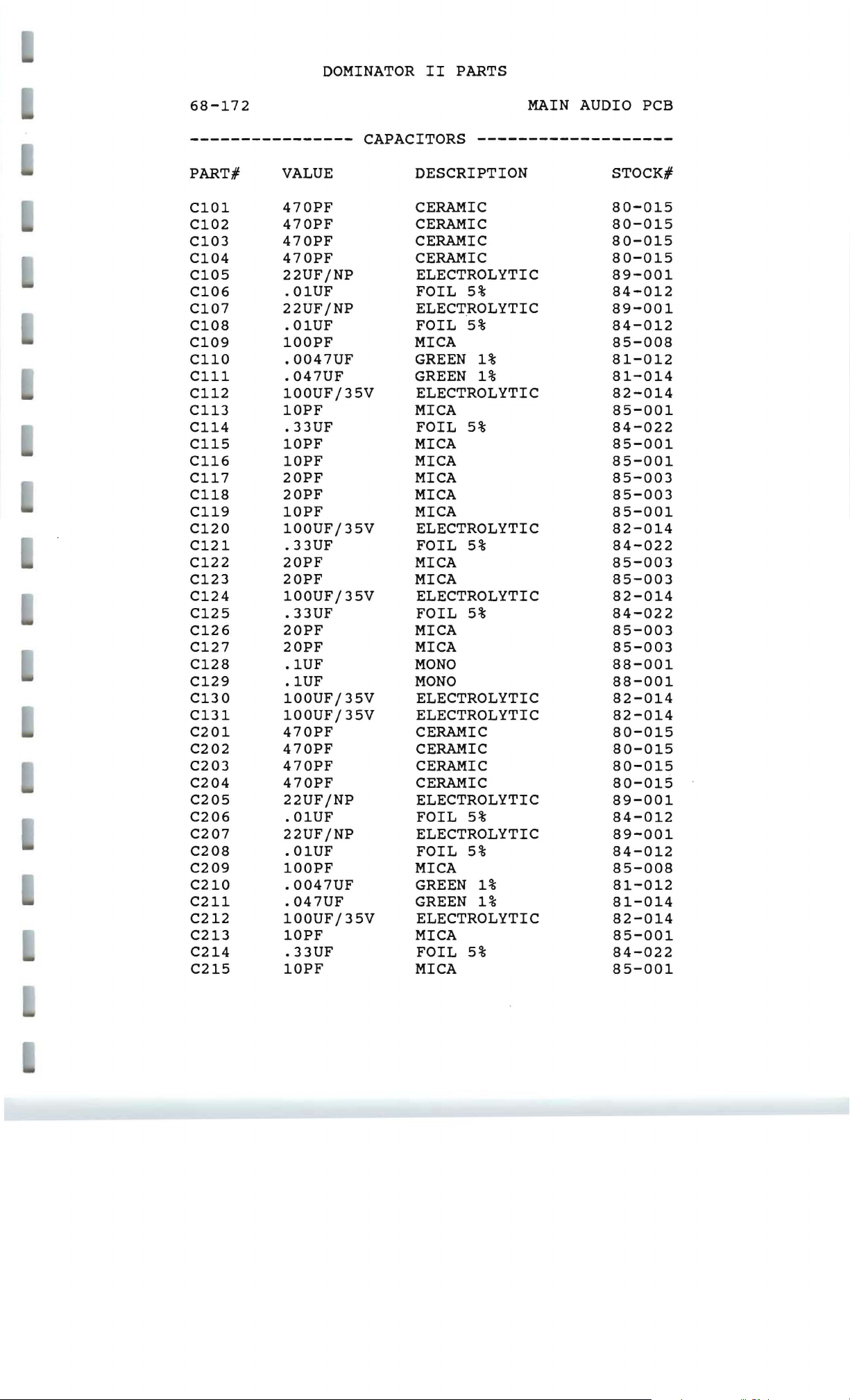
DOMINATOR
II
PARTS
68-172
----------------
PART #
C101
C102
C103
C104
C105
C106
C107
C108
C109
C110
C111
Cl12
Cl13
Cl14
Cl15
Cl16
Cl17
Cl18
Cl19
C120
C121
C122
C123
C124
C125
C126
C127
C128
C129
C130
C131
C201
C202
C203
C204
C205
C206
C207
C208
C209
C210
C211
C212
C213
C214
C215
VALUE
470PF
470PF
470PF
470PF
22UFjNP
.01UF
22UFjNP
.01UF
100PF
.0047UF
.047UF
100UFj35V
10PF
.33UF
10PF
10PF
20PF
20PF
10PF
100UFj35V
.33UF
20PF
20PF
100UFj35V
.33UF
20PF
20PF
.1UF
.1UF
100UFj35V
100UFj35V
470PF
470PF
470PF
470PF
22UFjNP
.01UF
22UFjNP
.01UF
100PF
.0047UF
.047UF
100UFj35V
10PF
.33UF
10PF
CAPACITORS
DESCRIPTION STOCK#
CERAMIC
CERAMIC
CERAMIC
CERAMIC
ELECTROLYTIC
FOIL
ELECTROLYTIC
FOIL
MICA
GREEN
GREEN
ELECTROLYTIC
MICA
FOIL
MICA
MICA
MICA
MICA
MICA
ELECTROLYTIC
FOIL
MICA
MICA
ELECTROLYTIC
FOIL
MICA
MICA
MONO
MONO
ELECTROLYTIC
ELECTROLYTIC
CERAMIC
CERAMIC
CERAMIC
CERAMIC
ELECTROLYTIC
FOIL
ELECTROLYTIC
FOIL
MICA
GREEN
GREEN
ELECTROLYTIC
MICA
FOIL
MICA
MAIN
AUDIO PCB
-------------------
80-015
80-015
80-015
80-015
89-001
5%
5%
1%
1%
5%
5%
5%
5%
5%
1%
1%
5%
84-012
89-001
84-012
85-008
81-012
81-014
82-014
85-001
84-022
85-001
85-001
85-003
85-003
85-001
82-014
84-022
85-003
85-003
82-014
84-022
85-003
85-003
88-001
88-001
82-014
82-014
80-015
80-015
80-015
80-015
89-001
84-012
89-001
84-012
85-008
81-012
81-014
82-014
85-001
84-022
85-001
Page 49
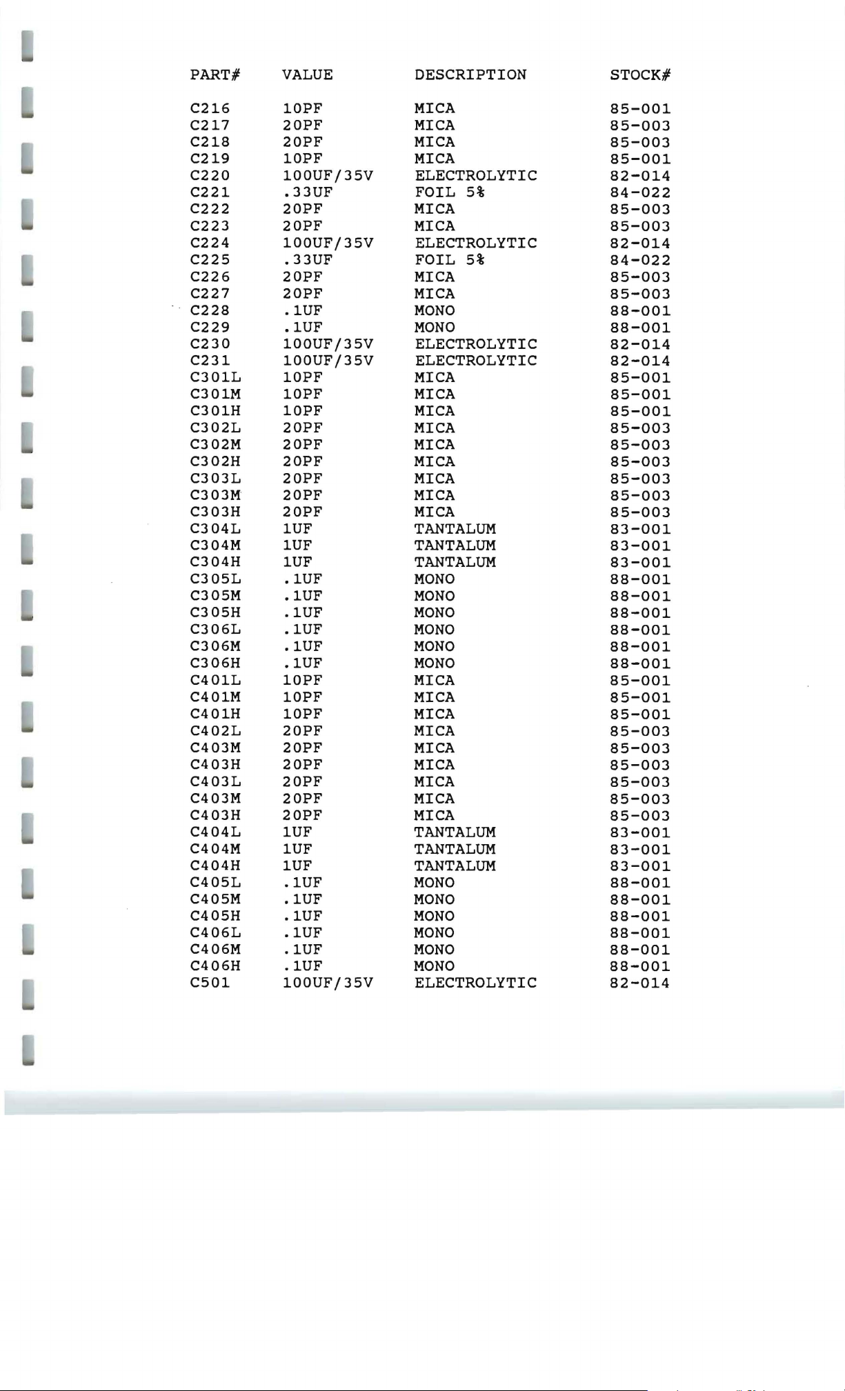
PART#
VALUE
DESCRIPTION
STOCK#
C216
C217
C218
C219
C220
C221
C222
C223
C224
C225
C226
C227
C228
C229
C230
C231
C301L
C301M
C301H
C302L
C302M
C302H
C303L
C303M
C303H
C304L
C304M 1UF
C304H
C305L
C305M
C305H
C306L
C306M
C306H
C401L
C401M
C401H
C402L
C403M
C403H
C403L
C403M
C403H
C404L
C404M 1UF
C404H
C405L
C405M
C405H
C406L
C406M
C406H
C501
10PF
20PF
20PF
10PF
100UF/35V
.33UF
20PF
20PF
100UF/35V
.33UF
20PF
20PF
.1UF
.1UF
100UF/35V
100UF/35V
10PF
10PF
10PF
20PF
20PF
20PF
20PF
20PF
20PF
1UF
1UF
.1UF
.1UF
.1UF
.1UF
.1UF
.1UF
10PF
10PF
10PF
20PF
20PF
20PF
20PF
20PF
20PF
1UF
1UF
.1UF
.1UF
.1UF
.1UF
.1UF
.1UF
100UF/35V
MICA
MICA
MICA
MICA
ELECTROLYTIC
FOIL
MICA
MICA
ELECTROLYTIC
FOIL
MICA
MICA
MONO
MONO
ELECTROLYTIC
ELECTROLYTIC
MICA
MICA
MICA
MICA
MICA
MICA
MICA
MICA
MICA
TANTALUM
TANTALUM
TANTALUM
MONO
MONO
MONO
MONO
MONO
MONO
MICA
MICA
MICA
MICA
MICA
MICA
MICA
MICA
MICA
TANTALUM
TANTALUM
TANTALUM
MONO
MONO
MONO
MONO
MONO
MONO
ELECTROLYTIC
5%
5%
85-001
85-003
85-003
85-001
82-014
84-022
85-003
85-003
82-014
84-022
85-003
85-003
88-001
88-001
82-014
82-014
85-001
85-001
85-001
85-003
85-003
85-003
85-003
85-003
85-003
83-001
83-001
83-001
88-001
88-001
88-001
88-001
88-001
88-001
85-001
85-001
85-001
85-003
85-003
85-003
85-003
85-003
85-003
83-001
83-001
83-001
88-001
88-001
88-001
88-001
88-001
88-001
82-014
Page 50

----------------
INDUCTORS
--------------------
PART #
L101
L102
L103
L104
L105
L106
L201
L202
L203
L204
L205
L206
VALUE
220UH
1000UH
220UH
1000UH
47UH
47UH
220UH
1000UH
220UH
1000UH
47UH
47UH
----------------
R101
R102
R103
R104
R105
R106
R107
R108
R109
R110
R111
Rl12
Rl13
Rl14
Rl15
Rl16
Rl17
Rl18
Rl19
R120
R121
R122
R123
R124
R125
R126
R127
R128
R129
R130
R131
R132
R133
R134
R135
1KOO
1KOO
407R
100R
4K99
1MOO
604R
10KO
10KO
10KO
10KO
4K99
20KO
23K7
33K2
33K2
3K74
13KO
24K3
3K74
13KO
24K3
10KO
10KO
10KO
10KO
10KO
10KO
10KO
4K99
10KO
4K99
10KO
6K34
15KO
DESCRIPTION
MOLDED
MOLDED
MOLDED
MOLDED
MOLDED
MOLDED
MOLDED
MOLDED
MOLDED
MOLDED
MOLDED
MOLDED
RESISTORS
1/4W
1/4W
1/4W
1/4W
1/4W
1/4W
1/2W
1/4W
1/4W
1/4W
1/4W
1/4W
1/4W
1/4W
1/4W
1/4W
1/4W
1/4W
1/4W
1/4W
1/4W
1/4W
1/4W
1/4W
1/4W
1/4W
1/4W
1/4W
1/4W
1/4W
1/4W
1/4W
1/4W
1/4W
1/4W
STOCK#
72-016
72-013
72-016
72-013
72-018
72-018
72-016
72-013
72-016
72-013
72-018
72-018
--------------------
1%
1%
1%
1%
1%
1%
1%
1%
1%
1%
1%
1%
1%
1%
1%
1%
1%
1%
1%
1%
1%
1%
1%
1%
1%
1%
1%
1%
1%
1%
1%
1%
1%
1%
1%
MTL
MTL
MTL
MTL
MTL
MTL
MTL
MTL
MTL
MTL
MTL
MTL
MTL
MTL
MTL
MTL
MTL
MTL
MTL
MTL
MTL
MTL
MTL
MTL
MTL
MTL
MTL
MTL
MTL
MTL
MTL
MTL
MTL
MTL
MTL
FILM
FILM
FILM
FILM
FILM
FILM
FILM
FILM
FILM
FILM
FILM
FILM
FILM
FILM
FILM
FILM
FILM
FILM
FILM
FILM
FILM
FILM
FILM
FILM
FILM
FILM
FILM
FILM
FILM
FILM
FILM
FILM
FILM
FILM
FILM
92-1001
92-1001
92-4070
92-1000
92-4991
92-1004
93-260
92-1002
92-1002
92-1002
92-1002
92-4991
92-2002
92-2372
92-3322
92-3322
92-3741
92-1302
92-2432
92-3741
92-1302
92-2432
92-1002
92-1002
92-1002
92-1002
92-1002
92-1002
92-1002
92-4991
92-1002
92-4991
92-1002
92-6341
92-1502
Page 51
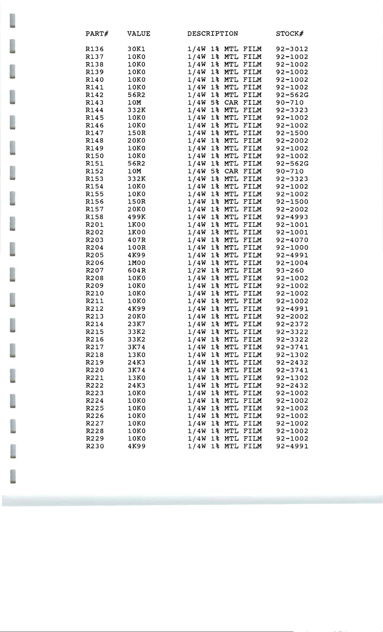
PART#
VALUE
DESCRIPTION
STOCK#
R136
R137
R138
R139
R140
R141
R142
R143
R144
R145
R146
R147
R148
R149
R150
R151
R152
R153
R154
R155
R156
R157
R158
R201
R202
R203
R204
R205
R206
R207
R208
R209
R210
R211
R212
R213
R214
R215
R216
R217
R218
R219
R220
R221
R222
R223
R224
R225
R226
R227
R228
R229
R230
30K1
10KO
10KO
10KO
10KO
10KO
56R2
10M
332K
10KO
10KO
150R
20KO
10KO
10KO
56R2
10M
332K
10KO
10KO
150R
20KO
499K
1KOO
1KOO
407R
100R
4K99
1MOO
604R
10KO
10KO
10KO
10KO
4K99
20KO
23K7
33K2
33K2
3K74
13KO
24K3
3K74
13KO
24K3
10KO
10KO
10KO
10KO
10KO
10KO
10KO
4K99
1/4W
1/4W
1/4W
1/4W
1/4W
1/4W
1/4W
1/4W
1/4W
1/4W
1/4W
1/4W
1/4W
1/4W
1/4W
1/4W
1/4W
1/4W
1/4W
1/4W
1/4W
1/4W
1/4W
1/4W
1/4W
1/4W
1/4W
1/4W
1/4W
1/2W
1/4W
1/4W
1/4W
1/4W
1/4W
1/4W
1/4W
1/4W
1/4W
1/4W
1/4W
1/4W
1/4W
1/4W
1/4W
1/4W
1/4W
1/4W
1/4W
1/4W
1/4W
1/4W
1/4W
1%
1%
1%
1%
1%
1%
1%
5%
1%
1%
1%
1%
1%
1%
1%
1%
5%
1%
1%
1%
1%
1%
1%
1%
1%
1%
1%
1%
1%
1%
1%
1%
1%
1%
1%
1%
1%
1%
1%
1%
1%
1%
1%
1%
1%
1%
1%
1%
1%
1%
1%
1%
1%
MTL
MTL
MTL
MTL
MTL
MTL
MTL
CAR
MTL
MTL
MTL
MTL
MTL
MTL
MTL
MTL
CAR
MTL
MTL
MTL
MTL
MTL
MTL
MTL
MTL
MTL
MTL
MTL
MTL
MTL
MTL
MTL
MTL
MTL
MTL
MTL
MTL
MTL
MTL
MTL
MTL
MTL
MTL
MTL
MTL
MTL
MTL
MTL
MTL
MTL
MTL
MTL
MTL
FILM
FILM
FILM
FILM
FILM
FILM
FILM
FILM
FILM
FILM
FILM
FILM
FILM
FILM
FILM
FILM
FILM
FILM
FILM
FILM
FILM
FILM
FILM
FILM
FILM
FILM
FILM
FILM
FILM
FILM
FILM
FILM
FILM
FILM
FILM
FILM
FILM
FILM
FILM
FILM
FILM
FILM
FILM
FILM
FILM
FILM
FILM
FILM
FILM
FILM
FILM
FILM
FILM
92-3012
92-1002
92-1002
92-1002
92-1002
92-1002
92-562G
90-710
92-3323
92-1002
92-1002
92-1500
92-2002
92-1002
92-1002
92-562G
90-710
92-3323
92-1002
92-1002
92-1500
92-2002
92-4993
92-1001
92-1001
92-4070
92-1000
92-4991
92-1004
93-260
92-1002
92-1002
92-1002
92-1002
92-4991
92-2002
92-2372
92-3322
92-3322
92-3741
92-1302
92-2432
92-3741
92-1302
92-2432
92-1002
92-1002
92-1002
92-1002
92-1002
92-1002
92-1002
92-4991
Page 52

PART #
VALUE
DESCRIPTION STOCK#
R231
R232
R233
R234
R235
R236
R237
R238
R239
R240
R241
R242
R243
R244
R245
R246
R247
R248
R249
R250
R251
R252
R253
R254
R255
R256
R257
R258
R301L
R301M
R301L
R302H
10KO
4K99
10KO
6K34
15KO
30K1
10KO
10KO
10KO
10KO
10KO
56R2
10M
332K
10KO
10KO
150R
20KO
10KO
10KO
56R2
10M
332K
10KO
10KO
150R
20KO
499K
10KO
10KO
10KO
10KO
R302M 10KO
R302L
R303H
10KO
4K99
R303M 4K99
R303L
R304H
4K99
4K99
R304M 4K99
R304L
R305H
R305M
R305L
R306H
R306M
R306L
R307H
R307M
R307L
R308H
R308M
R308L
R309H
4K99
5K90
5K90
5K90
5K90
5K90
5K90
1MOO
1MOO
1MOO
1KOO
1KOO
1KOO
21R5
1/4W
1/4W
1/4W
1/4W
1/4W
1/4W
1/4W
1/4W
1/4W
1/4W
1/4W
1/4W
1/4W
1/4W
1/4W
1/4W
1/4W
1/4W
1/4W
1/4W
1/4W
1/4W
1/4W
1/4W
1/4W
1/4W
1/4W
1/4W
1/4W
1/4W
1/4W
1/4W
1/4W
1/4W
1/4W
1/4W
1/4W
1/4W
1/4W
1/4W
1/4W
1/4W
1/4W
1/4W
1/4W
1/4W
1/4W
1/4W
1/4W
1/4W
1/4W
1/4W
1/4W
1%
1%
1%
1%
1%
1%
1%
1%
1%
1%
1%
1%
5%
1%
1%
1%
1%
1%
1%
1%
1%
5%
1%
1%
1%
1%
1%
1%
1%
1%
1%
1%
1%
1%
1%
1%
1%
1%
1%
1%
1%
1%
1%
1%
1%
1%
1%
1%
1%
1%
1%
1%
1%
MTL
MTL
MTL
MTL
MTL
MTL
MTL
MTL
MTL
MTL
MTL
MTL
CAR
MTL
MTL
MTL
MTL
MTL
MTL
MTL
MTL
CAR
MTL
MTL
MTL
MTL
MTL
MTL
MTL
MTL
MTL
MTL
MTL
MTL
MTL
MTL
MTL
MTL
MTL
MTL
MTL
MTL
MTL
MTL
MTL
MTL
MTL
MTL
MTL
MTL
MTL
MTL
MTL
FILM
FILM
FILM
FILM
FILM
FILM
FILM
FILM
FILM
FILM
FILM
FILM
FILM
FILM
FILM
FILM
FILM
FILM
FILM
FILM
FILM
FILM
FILM
FILM
FILM
FILM
FILM
FILM
FILM
FILM
FILM
FILM
FILM
FILM
FILM
FILM
FILM
FILM
FILM
FILM
FILM
FILM
FILM
FILM
FILM
FILM
FILM
FILM
FILM
FILM
FILM
FILM
FILM
92-1002
92-4991
92-1002
92-6341
92-1502
92-3012
92-1002
92-1002
92-1002
92-1002
92-1002
92-562G
90-710
92-3323
92-1002
92-1002
92-1500
92-2002
92-1002
92-1002
92-562G
90-710
92-3323
92-1002
92-1002
92-1500
92-2002
92-4993
92-1002
92-1002
92-1002
92-1002
92-1002
92-1002
92-4991
92-4991
92-4991
92-4991
92-4991
92-4991
92-5901
92-5901
92-5901
92-5901
92-5901
92-5901
92-1004
92-1004
92-1004
92-1001
92-1001
92-1001
92-215G
Page 53

PART #
VALUE
DESCRIPTION
STOCK#
R309M
R309L
R310H
R310M
R310L
R311H
R311M
R311L
R312H
R312M
R312L
R313H
21R5
21R5
40R2
40R2
40R2
40R2
40R2
40R2
200K
200K
200K
10KO
R313M 10KO
R313L
R314H
10KO
10KO
R314M 10KO
R314L
R315H
10KO
10KO
R315M 10KO
R315L
R316H
10KO
10KO
R316M 10KO
R316L
R317H
10KO
10KO
R317M 10KO
R317L
R318H
10KO
10KO
R318M 10KO
R318L
R319H
R319M
R319L
R320H
R320M
R320L
R401H
10KO
1M50
1M50
1M50
6K65
6K65
6K65
10KO
R401M 10KO
R401L
R402H
10KO
10KO
R402M 10KO
R402L
R403H
R403M
R403L
R404H
R404M
R404L
R405H
R405M
R405L
R406H
R406M
R406L
10KO
4K99
4K99
4K99
4K99
4K99
4K99
5K90
5K90
5K90
5K90
5K90
5K90
1/4W
1/4W
1/4W
1/4W
1/4W
1/4W
1/4W
1/4W
1/4W
1/4W
1/4W
1/4W
1/4W
1/4W
1/4W
1/4W
1/4W
1/4W
1/4W
1/4W
1/4W
1/4W
1/4W
1/4W
1/4W
1/4W
1/4W
1/4W
1/4W
1/4W
1/4W
1/4W
1/4W
1/4W
1/4W
1/4W
1/4W
1/4W
1/4W
1/4W
1/4W
1/4W
1/4W
1/4W
1/4W
1/4W
1/4W
1/4W
1/4W
1/4W
1/4W
1/4W
1/4W
1%
1%
1%
1%
1%
1%
1%
1%
1%
1%
1%
1%
1%
1%
1%
1%
1%
1%
1%
1%
1%
1%
1%
1%
1%
1%
1%
1%
1%
1%
1%
1%
1%
1%
1%
1%
1%
1%
1%
1%
1%
1%
1%
1%
1%
1%
1%
1%
1%
1%
1%
1%
1%
MTL
MTL
MTL
MTL
MTL
MTL
MTL
MTL
MTL
MTL
MTL
MTL
MTL
MTL
MTL
MTL
MTL
MTL
MTL
MTL
MTL
MTL
MTL
MTL
MTL
MTL
MTL
MTL
MTL
MTL
MTL
MTL
MTL
MTL
MTL
MTL
MTL
MTL
MTL
MTL
MTL
MTL
MTL
MTL
MTL
MTL
MTL
MTL
MTL
MTL
MTL
MTL
MTL
FILM
FILM
FILM
FILM
FILM
FILM
FILM
FILM
FILM
FILM
FILM
FILM
FILM
FILM
FILM
FILM
FILM
FILM
FILM
FILM
FILM
FILM
FILM
FILM
FILM
FILM
FILM
FILM
FILM
FILM
FILM
FILM
FILM
FILM
FILM
FILM
FILM
FILM
FILM
FILM
FILM
FILM
FILM
FILM
FILM
FILM
FILM
FILM
FILM
FILM
FILM
FILM
FILM
92-215G
92-215G
92-402G
92-402G
92-402G
92-402G
92-402G
92-402G
92-2003
92-2003
92-2003
92-1002
92-1002
92-1002
92-1002
92-1002
92-1002
92-1002
92-1002
92-1002
92-1002
92-1002
92-1002
92-1002
92-1002
92-1002
92-1002
92-1002
92-1002
92-1504
92-1504
92-1504
92-6651
92-6651
92-6651
92-1002
92-1002
92-1002
92-1002
92-1002
92-1002
92-4991
92-4991
92-4991
92-4991
92-4991
92-4991
92-5901
92-5901
92-5901
92-5901
92-5901
92-5901
Page 54
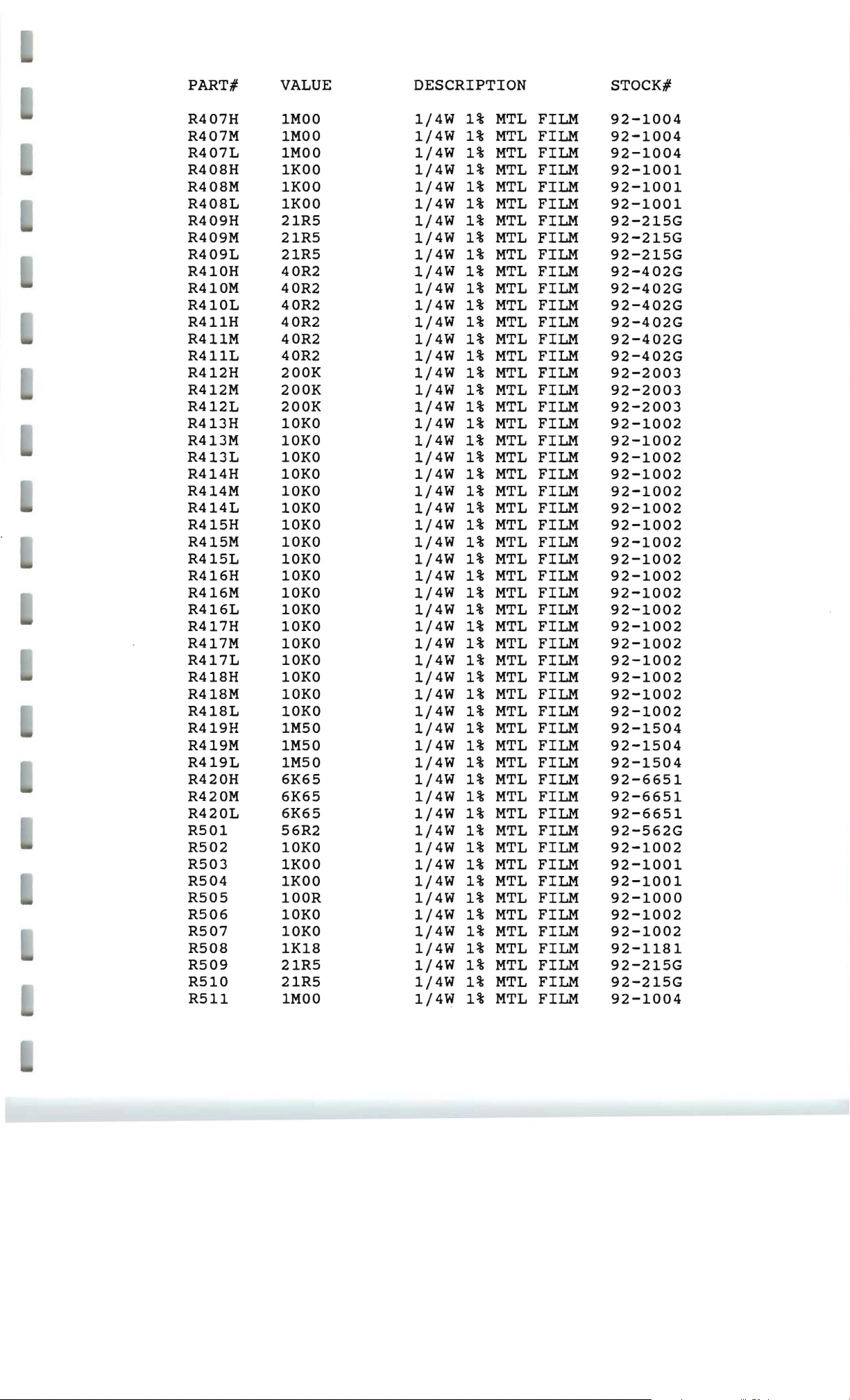
PART #
VALUE
DESCRIPTION
STOCK#
R407H
R407M
R407L
R408H
R408M
R408L
R409H
R409M
R409L
R410H
R410M
R410L
R411H
R411M
R411L
R412H
R412M
R412L
R413H
R413M 10KO
R413L
R414H
R414M
R414L
R415H
R415M 10KO
R415L
R416H
R416M
R416L
R417H
R417M
R417L
R418H 10KO
R418M 10KO
R418L
R419H
R419M 1M50
R419L
R420H 6K65
R420M 6K65
R420L
R501
R502
R503
R504
R505
R506
R507
R508
R509
R510
R511
1MOO
1MOO
1MOO
1KOO
1KOO
1KOO
21R5
21R5
21R5
40R2
40R2
40R2
40R2
40R2
40R2
200K
200K
200K
10KO
10KO
10KO
10KO
10KO
10KO
10KO
10KO
10KO
10KO
10KO
10KO
10KO
10KO
1M50
1M50
6K65
56R2
10KO
1KOO
1KOO
100R
10KO
10KO
1K18
21R5
21R5
1MOO
1/4W
1/4W
1/4W
1/4W
1/4W
1/4W
1/4W
1/4W
1/4W
1/4W
1/4W
1/4W
·
1/4W
1/4W
1/4W
1/4W
1/4W
1/4W
1/4W
1/4W
1/4W
1/4W
1/4W
1/4W
1/4W
1/4W
1/4W
1/4W
1/4W
1/4W
1/4W
1/4W
1/4W
1/4W
1/4W
1/4W
1/4W
1/4W
1/4W
1/4W
1/4W
1/4W
1/4W
1/4W
1/4W
1/4W
1/4W
1/4W
1/4W
1/4W
1/4W
1/4W
1/4W
1%
1%
1%
1%
1%
1%
1%
1%
1%
1%
1%
1%
1%
1%
1%
1%
1%
1%
1%
1%
1%
1%
1%
1%
1%
1%
1%
1%
1%
1%
1%
1%
1%
1%
1%
1%
1%
1%
1%
1%
1%
1%
1%
1%
1%
1%
1%
1%
1%
1%
1%
1%
1%
MTL
MTL
MTL
MTL
MTL
MTL
MTL
MTL
MTL
MTL
MTL
MTL
MTL
MTL
MTL
MTL
MTL
MTL
MTL
MTL
MTL
MTL
MTL
MTL
MTL
MTL
MTL
MTL
MTL
MTL
MTL
MTL
MTL
MTL
MTL
MTL
MTL
MTL
MTL
MTL
MTL
MTL
MTL
MTL
MTL
MTL
MTL
MTL
MTL
MTL
MTL
MTL
MTL
FILM
FILM
FILM
FILM
FILM
FILM
FILM
FILM
FILM
FILM
FILM
FILM
FILM
FILM
FILM
FILM
FILM
FILM
FILM
FILM
FILM
FILM
FILM
FILM
FILM
FILM
FILM
FILM
FILM
FILM
FILM
FILM
FILM
FILM
FILM
FILM
FILM
FILM
FILM
FILM
FILM
FILM
FILM
FILM
FILM
FILM
FILM
FILM
FILM
FILM
FILM
FILM
FILM
92-1004
92-1004
92-1004
92-1001
92-1001
92-1001
92-215G
92-215G
92-215G
92-402G
92-402G
92-402G
92-402G
92-402G
92-402G
92-2003
92-2003
92-2003
92-1002
92-1002
92-1002
92-1002
92-1002
92-1002
92-1002
92-1002
92-1002
92-1002
92-1002
92-1002
92-1002
92-1002
92-1002
92-1002
92-1002
92-1002
92-1504
92-1504
92-1504
92-6651
92-6651
92-6651
92-562G
92-1002
92-1001
92-1001
92-1000
92-1002
92-1002
92-1181
92-215G
92-215G
92-1004
Page 55

PART #
VALUE
DESCRIPTION
STOCK#
R512
R513
R514
RN101
RN201
-------------
VR101
VR102
VR103
VR104
VR105
VR201
VR202
VR203
VR204
VR205
VR301L
VR301M
VR301L
VR302H
VR302M
VR302L
VR303H
VR303M
VR303L
VR401H
VR401M
VR401L
VR402H
VR402M
VR402L
VR403H
VR403M
VR403L
VR501 15A10KX2
VR502 B10KX2
VR503 B10KX2
VR504
VR505
VR506 B10KX2
1MOO
1MOO
lOOK
10KI8
10KI8
VARIABLE
5K/10T
50K/1T
50K/1T
50K/1T
10K/1T
5K/10T
50K/1T
50K/1T
50K/1T
10K/1T
1K/1T
1K/1T
1K/1T
100R/1T
100R/1T
100R/1T
10K/1T
10K/1T
10K/1T
1K/1T
1K/1T
1K/1T
100R/1T
100R/1T
100R/1T
10K/1T
10K/1T
10K/1T
15A100KX2
15A10K
1/4W
1/4W
1/4W
4 RESISTOR
4 RESISTOR
10
PT6KV(5)
PT6KV(5)
PT6KV(5)
PT6KV(5)
10
PT6KV(5)
PT6KV(5)
PT6KV(5)
PT6KV(5)
PT6KV(5)
PT6KV(5)
PT6KV(5)
EVN36CAOOB12
EVN36CAOOB12
EVN36CAOOB12
PT6KV(5)
PT6KV(5)
PT6KV(5)
PT6KV(5)
PT6KV(5)
PT6KV(5)
EVN36CAOOB12
EVN36CAOOB12
EVN36CAOOB12
PT6KV(5)
PT6KV(5)
PT6KV(5)
DUAL
DUAL
DUAL
DUAL
10K
DUAL
1%
MTL
1%
MTL
1%
MTL
RESISTORS
TURN
TURN
10K
10K
10K
lOOK
AUD
10K
TRIM
TRIM
AUD
LIN
LIN
LIN
AUD
FILM
FILM
FILM
NET
NET
92-1004
92-1004
92-1003
97-004-18
97-004-18
---------------
22-020
22-033
22-033
22-033
22-032
22-020
22-033
22-033
22-033
22-032
22-030
22-030
22-030
22-034
22-034
22-034
22-032
22-032
22-032
22-030
22-030
22-030
22-034
22-034
22-034
22-032
22-032
22-032
23-061
23-062
23-062
23-064
23-063
23-062
---------------
D101
0102
0103
0104
0201
D202
D203
D204
1N914B
1N914B
1N914B
1N914B
1N914B
1N914B
1N914B
1N914B
SEMICONDUCTORS
SS DIODE
SS DIODE
SS DIODE
SS DIODE
SS DIODE
SS DIODE
SS DIODE
DIODE
SS
-----------------
30-002
30-002
30-002
30-002
30-002
30-002
30-002
30-002
Page 56

PART #
D301L
D301M
D301H
D302L
D302M
D302H
D303L
D303M
D303H
D401L
D401M
D401H
D402L
D402M
D402H
D403L
D403M
D403H
D501
D502
D503
LD501
LD502
LD503
LD504
LD505
LD506
LD507
LD508
LD509
LD510
Q301L
Q301M
Q301H
Q302L
Q302M
Q302H
Q401L
Q401M
Q401H
Q402L
Q402M
Q402H
Q501
Q502
Q503
Q504
Q505
U101
U102
U103
U104
U201
VALUE
1N914B
1N914B
1N914B
1N914B
1N914B
1N914B
1N914B
1N914B
1N914B
1N914B
1N914B
1N914B
1N914B
1N914B
1N914B
1N914B
1N914B
1N914B
1N4003
1N914B
1N914B
LTL-1234A
LTL-1204A
LTL-1234A
LTL-1204A
LTL-1234A
LTL-1204A
LTL-1234A
LTL-1204A
LTL-1234A
LTL-1204A
Jl13
Jl13
Jl13
2N3906
2N3906
2N3906
Jl13
Jl13
Jl13
2N3906
2N3906
2N3906
2N3904
2N3906
2N3906
2N3904
2N3904
NE5532
CD4016
NE5532
LF353
NE5532
DESCRIPTION
SS
DIODE
.
SS
DIODE
SS
DIODE
SS
DIODE
SS
DIODE
SS
DIODE
SS
DIODE
SS
DIODE
SS
DIODE
SS
DIODE
SS
DIODE
SS
DIODE
SS
DIODE
SS
DIODE
SS
DIODE
SS
DIODE
SS
DIODE
SS
DIODE
POWER
SS
SS
RED
GREEN
RED
GREEN
RED
GREEN
RED
GREEN
RED
GREEN
CH
N
N
CH
CH
N
DIODE
DIODE
DIODE
LED
LED
LED
LED
LED
LED
LED
LED
LED
LED
FET
FET
FET
PNP
PNP
PNP
CH
CH
CH
FET
FET
FET
N
N
N
PNP
PNP
PNP
NPN
PNP
PNP
NPN
NPN
DUAL
CMOS
DUAL
DUAL
DUAL
LN
OPAMP
SWITCH
LN
OPAMP
OPAMP
LN
OPAMP
STOCK#
30-002
30-002
30-002
.
30-002
30-002
30-002
30-002
30-002
30-002
30-002
30-002
30-002
30-002
30-002
30-002
30-002
30-002
30-002
30-009
30-002
30-002
27-034
27-035
27-034
27-035
27-034
27-035
27-034
27-035
27-034
27-035
31-010
31-010
31-010
31-011
31-011
31-011
31-010
31-010
31-010
31-011
31-011
31-011
31-015
31-011
31-011
31-015
31-015
32-028
38-003
32-028
32-007
32-028
!\
Page 57
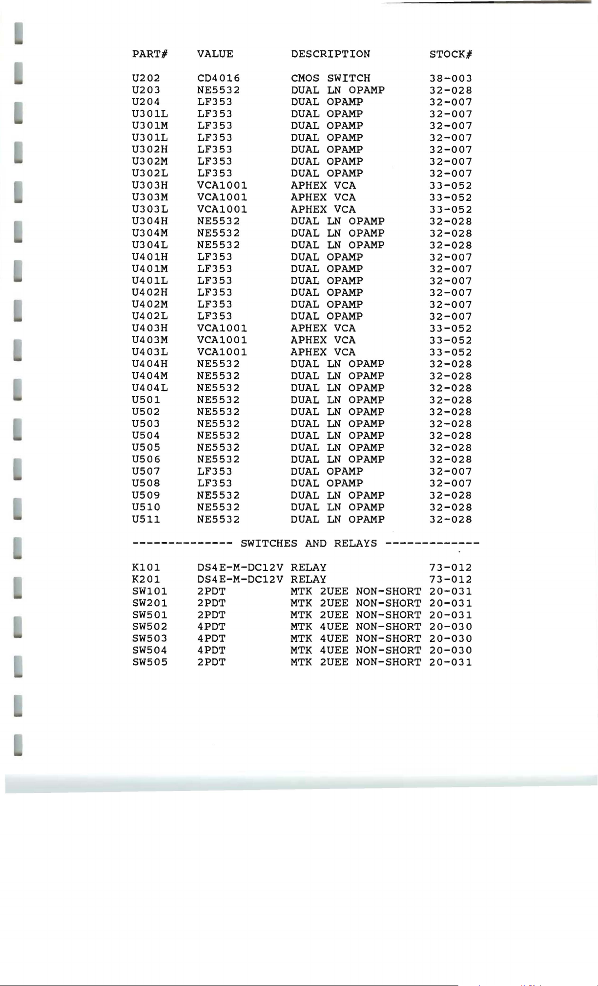
PART #
VALUE
DESCRIPTION STOCK#
U202
U203
U204
U301L
U301M
U301L
U302H
U302M
U302L
U303H VCA1001
U303M VCA1001
U303L
U304H
U304M
U304L
U401H
U401M
U401L
U402H
U402M
U402L
U403H
U403M VCA1001
U403L
U404H
U404M
U404L
U501
U502
U503
U504
U505
U506
U507
U508
U509
U510
U511
CD4016
NE5532
LF353
LF353
LF353
LF353
LF353
LF353
LF353
VCA1001
NE5532
NE5532
NE5532
LF353
LF353
LF353
LF353
LF353
LF353
VCA1001
VCA1001
NE5532
NE5532
NE5532
NE5532
NE5532
NE5532
NE5532
NE5532
NE5532
LF353
LF353
NE5532
NE5532
NE5532
CMOS
DUAL
DUAL
DUAL
DUAL
DUAL
DUAL
DUAL
DUAL
APHEX
APHEX
APHEX
DUAL
DUAL
DUAL
DUAL
DUAL
DUAL
DUAL
DUAL
DUAL
APHEX
APHEX
APHEX
DUAL
DUAL
DUAL
DUAL
DUAL
DUAL
DUAL
DUAL
DUAL
DUAL
DUAL
DUAL
DUAL
DUAL
SWITCH
LN
OPAMP
OPAMP
OPAMP
OPAMP
OPAMP
OPAMP
OPAMP
OPAMP
VCA
VCA
VCA
LN
OPAMP
LN
OPAMP
LN
OPAMP
OPAMP
OPAMP
OPAMP
OPAMP
OPAMP
OPAMP
VCA
VCA
VCA
LN
OPAMP
LN
OPAMP
LN
OPAMP
LN
OPAMP
LN
OPAMP
LN
OPAMP
LN
OPAMP
LN
OPAMP
LN
OPAMP
OPAMP
OPAMP
LN
OPAMP
LN
OPAMP
LN
OPAMP
38-003
32-028
32-007
32-007
32-007
32-007
32-007
32-007
32-007
33-052
33-052
33-052
32-028
32-028
32-028
32-007
32-007
32-007
32-007
32-007
32-007
33-052
33-052
33-052
32-028
32-028
32-028
32-028
32-028
32-028
32-028
32-028
32-028
32-007
32-007
32-028
32-028
32-028
--------------
K101
K201
SW101
SW201 2PDT
SW501
SW502
SW503
SW504 4PDT
SW505
DS4E-M-DC12V
DS4E-M-DC12V
2PDT
2PDT
4PDT
4PDT
2PDT
SWITCHES
RELAY
RELAY
MTK
MTK
MTK
MTK
MTK
MTK
MTK
RELAYS
AND
2UEE NON-SHORT
2UEE NON-SHORT
2UEE NON-SHORT
4UEE NON-SHORT
4UEE NON-SHORT
4UEE NON-SHORT
2UEE NON-SHORT
-------------
73-012
73-012
20-031
20-031
20-031
20-030
20-030
20-030
20-031
Page 58

------------------
PART
#
VALUE
CONNECTORS
------------------
DESCRIPTION STOCK#
TP101
TP102
TP201
TP301L
TP301M
TP301L
TP302H
TP302M
TP302L
TP401H
TP401M
TP401L
TP402H
TP402M
TP402L
H501
H502
H503
H504
H505
J101
J102
J201
J202
J501
TP-101-20
TP-101-20
TP-101-20
TP-101-20
TP-101-20
TP-101-20
TP-101-20
TP-101-20
TP-101-20
TP-101-20
TP-101-20
TP-101-20
TP-101-20
TP-101-20
TP-101-20
TEST POINT
TEST POINT
TEST POINT
TEST POINT
TEST POINT
TEST POINT
TEST POINT
TEST
TEST POINT
TEST POINT
TEST POINT
TEST
TEST POINT
TEST POINT
TEST POINT
M100 8
M100 8
M100
10
M100 3
22-23-2031
RAPC3FG
RAPC3MHG
RAPC3FG
RAPC3MHG
520250-2
3
XLR-3F
XLR-3M
XLR-3F
XLR-3M
RJ11
PIN
PIN
PIN
PIN
PIN
POINT
POINT
SIP
SIP
SIP
SIP
MOLEX
4
PIN
HEADER
HEADER
HEADER
HEADER
JACK
67-046
67-046
67-046
67-046
67-046
67-046
67-046
67-046
67-046
67-046
67-046
67-046
67-046
67-046
67-046
43-063
43-063
43-063
43-063
43-093
43-074
43-073
43-074
43-073
42-020
-----------------
QTY
35
2
6
10
1
1
MISCELLANEOUS
DESCRIPTION
8
PIN
14
18
PIN
PIN
DIP
DIP
DIP
IC
IC
IC
BIVAR SPACER
PRINTED
TT-02
CIRCUIT
SHUNT
SOCKET
SOCKET
SOCKET
BOARD
----------------
STOCK#
43-003
43-004
43-008
62-050
68-172A
67-065
Page 59

DOMINATOR
II
PARTS
68-176
----------------
PART
Cl
C2
#
VALUE
22UF/25V
22UF/25V
----------------
Rl
R2
R3
-------------
VRI
-------~-------
Ul
150R
lKOO
lKOO
VARIABLE RESISTORS
10K/IT
SEMICONDUCTORS
LM3914
LEDI MV54164
CAPACITORS
DESCRIPTION STOCK#
ELECTROLYTIC
ELECTROLYTIC
RESISTORS
1/4W
1/4W
1/4W
PTI0H
LED
GI
LED
DISPLAY/SWITCH
-------------------
--------------------
1%
1%
1%
MTL
MTL
MTL
FILM
FILM
FILM
---------------
-----------------
BAR
DRIVER
BAR
PCB
82-003
82-003
92-1500
92-1001
92-1001
22-014
33-023
27-038
------------------
SWI
Al12-03-RNCQE
-----------------
HI
---------------
QTY
1
1
DESCRIPTION STOCK#
18
PRINTED CIRCUIT
SWITCHES
CONNECTORS
MISCELLANEOUS
PIN
DIP
IC
C&K
12
16
CONDUCTOR
SOCKET
BOARD
--------------------
POS
ROTARY
-------------------
------------------
21-011
54-059
43-008
68-176B
Page 60

DOMINATOR
II
PARTS
68-177
----------------
PART #
C1
C2
C3
C4
C5
C6
C7
C8
C9
C10
C11
C12
C13
C14
C15
VALUE
.01UF
.01UF
.1UF
.1UF
.33UF
.001UF
22UF/25V
.1UF
.0047UF
.0047UF
.1UF
.1UF
.1UF
.1UF
.1UF
----------------
CAPACITORS
DESCRIPTION STOCK#
FOIL
FOIL
FOIL
FOIL
FOIL
FOIL
ELECTROLYTIC
FOIL
FOIL
FOIL
FOIL
MONO
MONO
MONO
MONO
RESISTORS
AUX
CONTROL
-------------------
84-012
84-012
84-043
84-043
84-022
84-001
82-003
84-043
84-007
84-007
84-043
88-001
88-001
88-001
88-001
--------------------
PCB
R1
R2
R3
R4
R5
R6
R7
R8
R9
R10
R11
R12
R13
R14
R15
R16
R17 45K3
R18
R19
R20
R21
R22
R23
R24
R25 11KO
R26 49K9
R27 11KO
R28
R29 10KO
249K
ZERO
205K
ZERO
165K
2K94
133K
3K32
110K
1K02
88K7
750R
71K5
133R
57K6
249R
976R
36K5
442R
29K4
51R1
23K2
402R
11KO
1/4W
1/4W
1/4W
1/4W
1/4W
1/4W
1/4W
1/4W
1/4W
1/4W
1/4W
1/4W
1/4W
1/4W
1/4W
1/4W
1/4W
1/4W
1/4W
1/4W
1/4W
1/4W
1/4W
1/4W
1/4W
1/4W
1/4W
1%
1%
1%
1%
1%
1%
1%
1%
1%
1%
1%
1%
1%
1%
1%
1%
1%
1%
1%
1%
1%
1%
1%
1%
1%
1%
1%
MTL
MTL
MTL
MTL
MTL
MTL
MTL
MTL
MTL
MTL
MTL
MTL
MTL
MTL
MTL
MTL
MTL
MTL
MTL
MTL
MTL
MTL
MTL
MTL
MTL
MTL
MTL
FILM
FILM
FILM
FILM
FILM
FILM
FILM
FILM
FILM
FILM
FILM
FILM
FILM
FILM
FILM
FILM
FILM
FILM
FILM
FILM
FILM
FILM
FILM
FILM
FILM
FILM
FILM
92-2493
92-2053
92-1653
92-2941
92-1333
92-3321
92-1103
92-1021
92-8872
92-7500
92-7152
92-1330
92-5762
92-2490
92-4532
92-9760
92-3652
92-4420
92-2942
92-511G
92-2322
92-4020
92-1102
92-4992
92-1102
92-1102
92-1002
Page 61
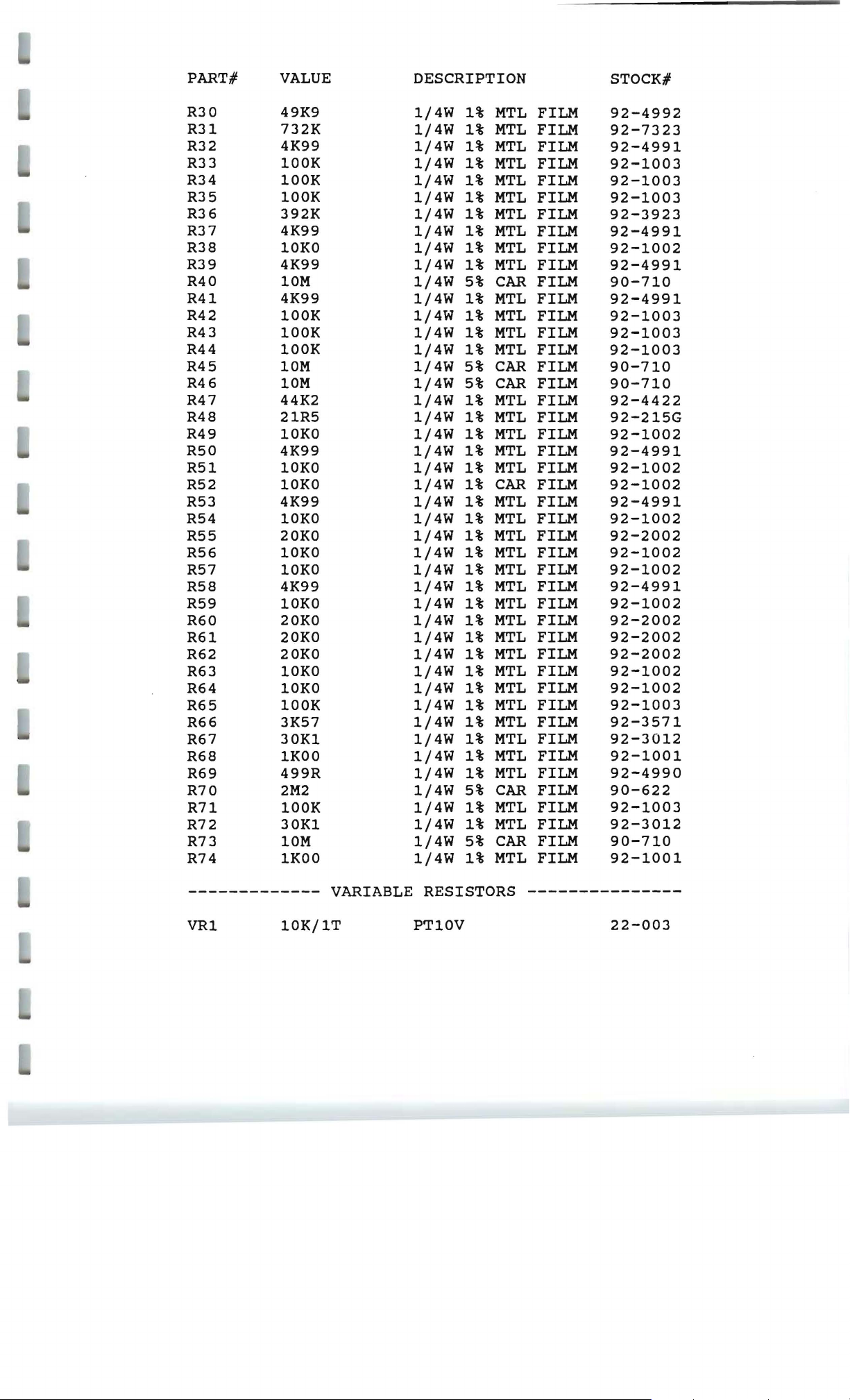
PART #
VALUE
DESCRIPTION
STOCK#
R30
R31
R32 4K99
R33 lOOK
R34
R35 lOOK
R36
R37 4K99
R38
R39 4K99
R40
R41
R42 lOOK
R43 lOOK
R44 lOOK
R45
R46 10M
R47 44K2
R48
R49 10KO
R50
R51
R52 10KO
R53
R54 10KO
R55 20KO
R56
R57 10KO
R58 4K99
R59 10KO
R60
R61
R62 20KO
R63
R64 10KO
R65
R66 3K57
R67
R68
R69
R70
R71
R72
R73 10M
R74
49K9
732K
lOOK
392K
10KO
10M
4K99
10M
21R5
4K99
10KO
4K99
10KO
20KO
20KO
10KO
lOOK
30K1
1KOO
499R
2M2
lOOK
30K1
1KOO
1/4W
1/4W
1/4W
1/4W
1/4W
1/4W
1/4W
1/4W
1/4W
1/4W
1/4W
1/4W
1/4W
1/4W
1/4W
1/4W
1/4W
1/4W
1/4W
1/4W
1/4W
1/4W
1/4W
1/4W
1/4W
1/4W
1/4W
1/4W
1/4W
1/4W
1/4W
1/4W
1/4W
1/4W
1/4W
1/4W
1/4W
1/4W
1/4W
1/4W
1/4W
1/4W
1/4W
1/4W
1/4W
1%
1%
1%
1%
1%
1%
1%
1%
1%
1%
5%
1%
1%
1%
1%
5%
5%
1%
1%
1%
1%
1%
1%
1%
1%
1%
1%
1%
1%
1%
1%
1%
1%
1%
1%
1%
1%
1%
1%
1%
5%
1%
1%
5%
1%
MTL
MTL
MTL
MTL
MTL
MTL
MTL
MTL
MTL
MTL
CAR
MTL
MTL
MTL
MTL
CAR
CAR
MTL
MTL
MTL
MTL
MTL
CAR
MTL
MTL
MTL
MTL
MTL
MTL
MTL
MTL
MTL
MTL
MTL
MTL
MTL
MTL
MTL
MTL
MTL
CAR
MTL
MTL
CAR
MTL
FILM
FILM
FILM
FILM
FILM
FILM
FILM
FILM
FILM
FILM
FILM
FILM
FILM
FILM
FILM
FILM
FILM
FILM
FILM
FILM
FILM
FILM
FILM
FILM
FILM
FILM
FILM
FILM
FILM
FILM
FILM
FILM
FILM
FILM
FILM
FILM
FILM
FILM
FILM
FILM
FILM
FILM
FILM
FILM
FILM
92-4992
92-7323
92-4991
92-1003
92-1003
92-1003
92-3923
92-4991
92-1002
92-4991
90-710
92-4991
92-1003
92-1003
92-1003
90-710
90-710
92-4422
92-215G
92-1002
92-4991
92-1002
92-1002
92-4991
92-1002
92-2002
92-1002
92-1002
92-4991
92-1002
92-2002
92-2002
92-2002
92-1002
92-1002
92-1003
92-3571
92-3012
92-1001
92-4990
90-622
92-1003
92-3012
90-710
92-1001
-------------
VR1
10K/1T
VARIABLE RESISTORS
PT10V
---------------
22-003
Page 62

---------------
SEMICONDUCTORS
-----------------
PART #
D1
D2
D3
D4
D5
D6
D7
D8
D9
D10
D11
D12
D13
D14
D15
D16
D17
D18
LD1
Q1
Q2
Q3
Q4
QA1
U1
U2
U3
U4
U5
VALUE
1N914B
1N914B
1N914B
1N914B
1N914B
1N914B
1N914B
1N914B
1N914B
1N914B
1N914B
1N914B
1N914B
1N914B
1N914B
1N914B
1N914B
1N914B
SLR-34-MG3
2N3906
2N3904
2N3904
2N3906
CA3086
LF347
LM311
LF347
MC34084
LF347
DESCRIPTION STOCK#
SS DIODE
SS DIODE
SS DIODE
DIODE
SS
SS DIODE
DIODE
SS
SS DIODE
SS DIODE
SS DIODE
DIODE
SS
SS DIODE
SS DIODE
SS DIODE
SS DIODE
SS DIODE
SS
DIODE
SS
DIODE
SS
DIODE
GREEN
PNP
NPN
NPN
PNP
TRANSISTOR
QUAD
COMPARATOR
QUAD
QUAD
QUAD
LED
OPAMP
OPAMP
OPAMP
OPAMP
T-1
ARRAY
30-002
30-002
30-002
30-002
30-002
30-002
30-002
30-002
30-002
30-002
30-002
30-002
30-002
30-002
30-002
30-002
30-002
30-002
27-017
31-011
31-015
31-015
31-011
33-022
32-048
33-002
32-048
36-027
32-048
------------------
H101
H102
H103
H104
----------------QTY
1 8
5
1
M100 8
M100
22-23-2031
3916-0000T
DESCRIPTION STOCK#
PIN
PIN
14
PRINTED
CONNECTORS
PIN
8
PIN
PIN
3
3M
MISCELLANEOUS
DIP
IC
DIP
IC
CIRCUIT
SOCKET
SOCKET
------------------
SIP
SIP
MOLEX
HEADER
BOARD
SOCKET
SOCKET
RTANGL
16
PIN
43-063
43-063
43-094
41-046
----------------
43-003
43-004
68-177A
Page 63

DOMINATOR
II
PARTS
68-178
---------------PART
#
C1
C2
C3
C4
C5
----------------
R1
R2
-------------
VR1
---------------
BR1
01
02
U1
U2
CAPACITORS
VALUE
2200UF/35V
2200UF/35V
1UF/35V
1UF/35V
22UF/25V
RESISTORS
121R
1K27
VARIABLE RESISTORS
100R/1T
SEMICONDUCTORS
RS202L
1N4003
1N4003
LM7815
LM337T
POWER
-------------------
DESCRIPTION
SNAP-IN
SNAP-IN
ELEC
ELEC
TANTALUM
TANTALUM
ELECTROLYTIC
--------------------
1/4W
1/4W
1%
1%
MTL
MTL
PT10V
-----------------
BRIDGE
POWER
POWER
REGULATOR
REGULATOR
RECTIFIER
DIODE
DIODE
+15V
-ADJ
SUPPLY
FILM
FILM
---------------
PCB
STOCK#
82-040
82-040
83-001
83-001
82-003
92-1210
92-1271
22-009
30-004
30-009
30-009
36-009
36-030
------------------
H1
H2
H3
H4
22-23-2071
22-23-2031
22-23-2031
22-23-2031
-----------------
QTY
1 PRINTED CIRCUIT
DESCRIPTION STOCK#
CONNECTORS
7
3
3
3
MISCELLANEOUS
PIN
PIN
PIN
PIN
BOARD
------------------
MOLEX
MOLEX
MOLEX
MOLEX
----------------
43-062
43-093
43-093
43-093
68-178A
Page 64

DOMINATOR
II
PARTS
68-179
----------------
PART #
C1
C2
C3
C4
C5
C6
C7
C8
----------------
R1 4K99
R2
R3
R4
R5
R6
R7
R8
R9
R10
R11
R12
R13 10KO
R14
R15
R16
R17 10KO
R18 10KO
R19
R20
R21
R22 10KO
R23 10KO
VALUE
39PF
20PF
20PF
39PF
20PF
20PF
.1UF
.1UF
4K99
10KO
10KO
49K9
2K49
10KO
10KO
2K49
49K9
4K99
4K99
10KO
49K9
2K49
2K49
49K9
10KO
CAPACITORS
DESCRIPTION
MICA
MICA
MICA
MICA
MICA
MICA
MONO
MONO
RESISTORS
1/4W
1/4W
1/4W
1/4W
1/4W
1/4W
1/4W
1/4W
1/4W
1/4W
1/4W
1/4W
1/4W
1/4W
1/4W
1/4W
1/4W
1/4W
1/4W
1/4W
1/4W
1/4W
1/4W
CLIPPER
PCB
-------------------
STOCK#
85-004
85-003
85-003
85-004
85-003
85-003
88-001
88-001
--------------------
1%
1%
1%
1%
1%
1%
1%
1%
1%
1%
1%
1%
1%
1%
1%
1%
1%
1%
1%
1%
1%
1%
1%
MTL
MTL
MTL
MTL
MTL
MTL
MTL
MTL
MTL
MTL
MTL
MTL
MTL
MTL
MTL
MTL
MTL
MTL
MTL
MTL
MTL
MTL
MTL
FILM
FILM
FILM
FILM
FILM
FILM
FILM
FILM
FILM
FILM
FILM
FILM
FILM
FILM
FILM
FILM
FILM
FILM
FILM
FILM
FILM
FILM
FILM
92-4991
92-4991
92-1002
92-1002
92-4992
92-2491
92-1002
92-1002
92-2491
92-4992
92-4991
92-4991
92-1002
92-1002
92-4992
92-2491
92-1002
92-1002
92-2491
92-4992
92-1002
92-1002
92-1002
---------------
Q1
Q2
QA1
QA2
U1
U2
2N3906
2N3906
CA3096 TRANSISTOR
CA3096
LF353
LF353
SEMICONDUCTORS
PNP
PNP
TRANSISTOR
DUAL
DUAL
OPAMP
OPAMP
-----------------
31-011
31-011
ARRAY
ARRAY
33-026
33-026
32-007
32-007
Page 65
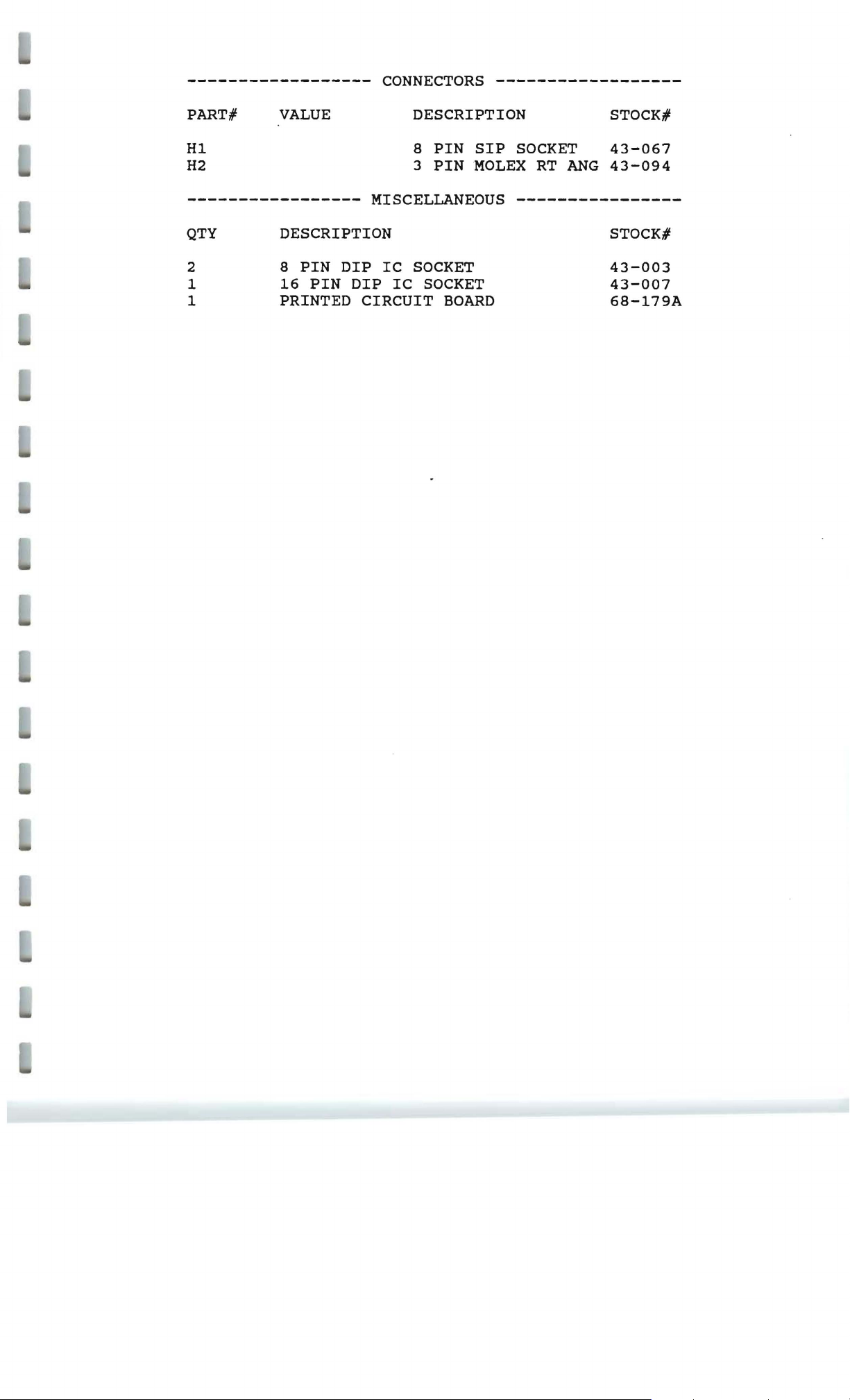
------------------
CONNECTORS
------------------
PART
#
VALUE
DESCRIPTION
HI 8
H2
-----------------
QTY
2
1
1 PRINTED CIRCUIT
DESCRIPTION STOCK#
8
PIN
16
PIN
MISCELLANEOUS
DIP
DIP
IC
IC
3
SOCKET
PIN
SIP
PIN
MOLEX
SOCKET
BOARD
SOCKET
RT
ANG
----------------
STOCK#
43-067
43-094
43-003
43-007
68-179A
Page 66
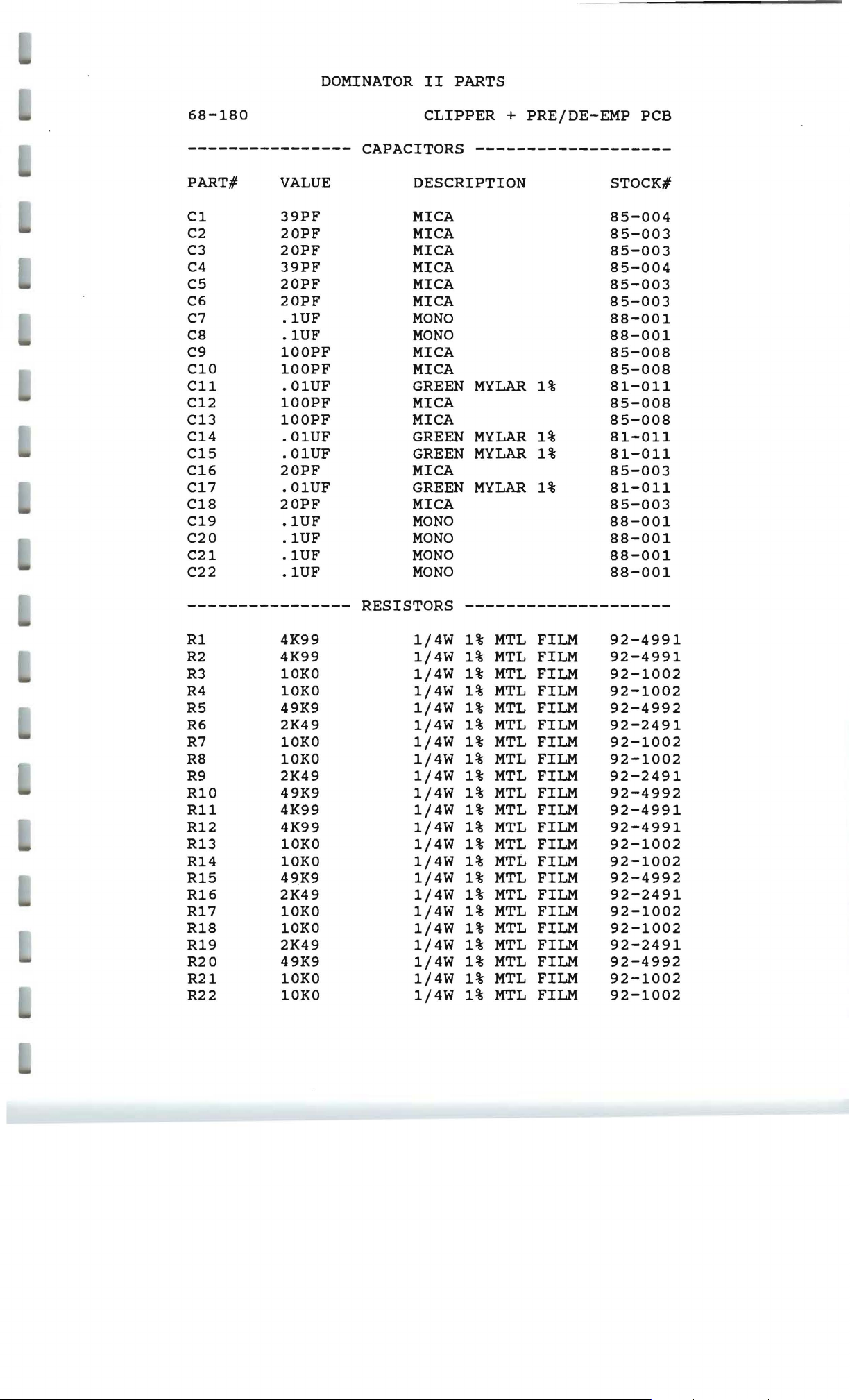
DOMINATOR
II
PARTS
68-180
----------------
PART#
C1
C2
C3
C4
C5
C6
C7
C8
C9
C10
C11
C12
C13
C14
C15
C16
C17
C18
C19
C20
C21
C22
VALUE
39PF
20PF
20PF
39PF
20PF
20PF
.1UF
.1UF
100PF
100PF
.01UF
100PF
100PF
.01UF
.01UF
20PF
.01UF
20PF
.1UF
.1UF
.1UF
.1UF
CLIPPER
CAPACITORS
DESCRIPTION
MICA
MICA
MICA
MICA
MICA
MICA
MONO
MONO
MICA
MICA
GREEN
MICA
MICA
GREEN
GREEN
MICA
GREEN
MICA
MONO
MONO
MONO
MONO
+
PRE/DE-EMP
-------------------
MYLAR
MYLAR
MYLAR
MYLAR
1%
1%
1%
1%
PCB
STOCK#
85-004
85-003
85-003
85-004
85-003
85-003
88-001
88-001
85-008
85-008
81-011
85-008
85-008
81-011
81-011
85-003
81-011
85-003
88-001
88-001
88-001
88-001
----------------
R1
R2
R3
R4 10KO
R5 49K9
R6
R7
R8
R9
R10
R11
R12
R13 10KO
R14
R15
R16
R17 10KO
R18
R19
R20
R21
R22
4K99
4K99
10KO
2K49
10KO
10KO
2K49
49K9
4K99
4K99
10KO
49.K9
2K49
10KO
2K49
49K9
10KO
10KO
RESISTORS
1/4W
1/4W
1/4W
1/4W
1/4W
1/4W
1/4W
1/4W
1/4W
1/4W
1/4W
1/4W
1/4W
1/4W
1/4W
1/4W
1/4W
1/4W
1/4W
1/4W
1/4W
1/4W
--------------------
1%
1%
1%
1%
1%
1%
1%
1%
1%
1%
1%
1%
1%
1%
1%
1%
1%
1%
1%
1%
1%
1%
MTL
MTL
MTL
MTL
MTL
MTL
MTL
MTL
MTL
MTL
MTL
MTL
MTL
MTL
MTL
MTL
MTL
MTL
MTL
MTL
MTL
MTL
FILM
FILM
FILM
FILM
FILM
FILM
FILM
FILM
FILM
FILM
FILM
FILM
FILM
FILM
FILM
FILM
FILM
FILM
FILM
FILM
FILM
FILM
92-4991
92-4991
92-1002
92-1002
92-4992
92-2491
92-1002
92-1002
92-2491
92-4992
92-4991
92-4991
92-1002
92-1002
92-4992
92-2491
92-1002
92-1002
92-2491
92-4992
92-1002
92-1002
Page 67
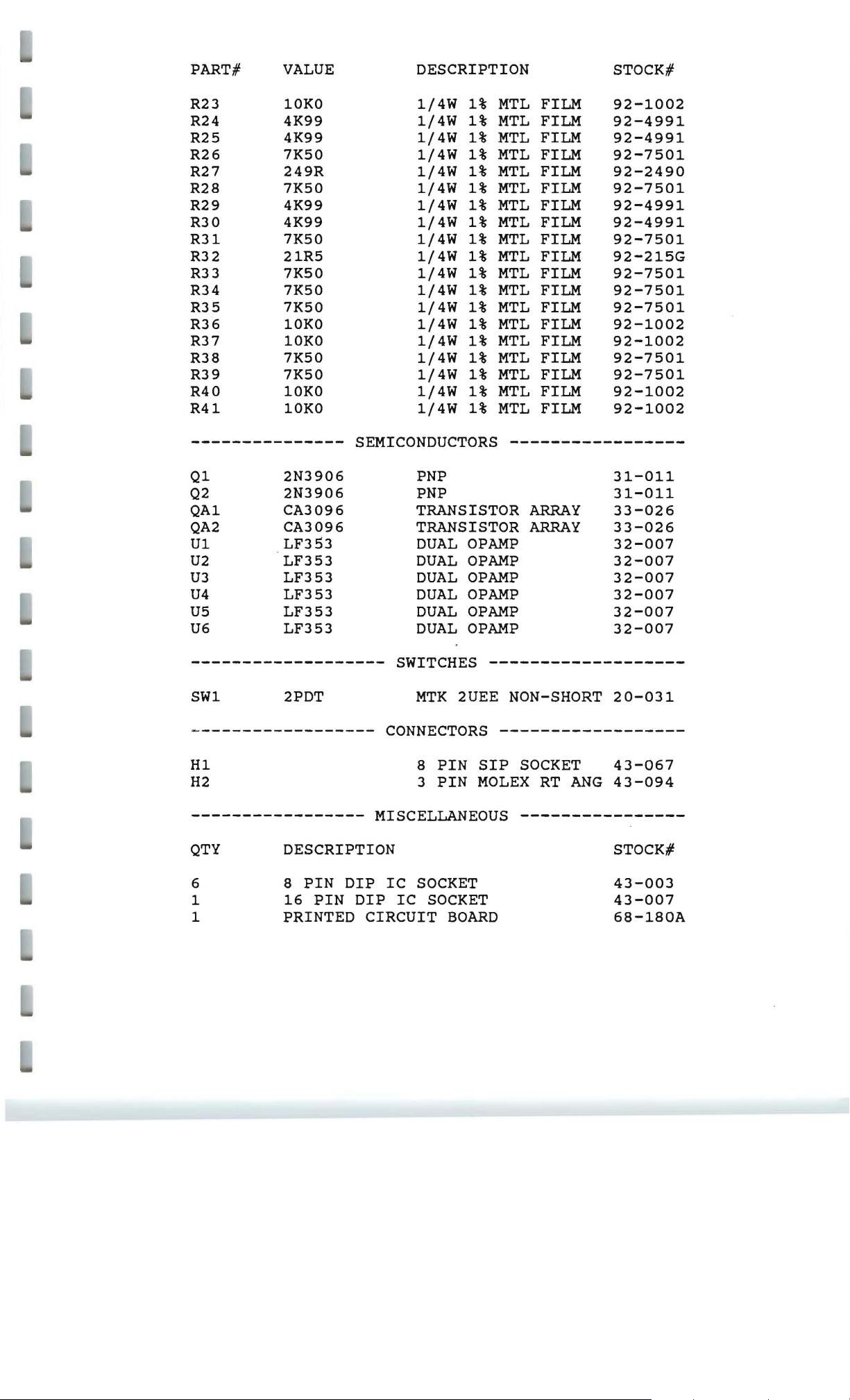
PART#
VALUE
DESCRIPTION
STOCK#
R23
R24
R25
R26
R27
R28
R29
10KO
4K99
4K99
7K50
249R
7K50
4K99
R30 4K99
R31
R32
R33
7K50
21R5
7K50
R34 7K50
R35
R36
7K50
10KO
R37 10KO
R38
R39
R40
R41
7K50
7K50
10KO
10KO
--------------Q1
Q2
QA1
QA2
U1
U2
U3
U4
U5
U6
2N3906
2N3906
CA3096
CA3096
LF353
LF353
LF353
LF353
LF353
LF353
1/4W
1/4W
1/4W
1/4W
1/4W
1/4W
1/4W
1/4W
1/4W
1/4W
1/4W
1/4W
1/4W
1/4W
1/4W
1/4W
1/4W
1/4W
1/4W
1%
1%
1%
1%
1%
1%
1%
1%
1%
1%
1%
1%
1%
1%
1%
1%
1%
1%
1%
SEMICONDUCTORS
PNP
PNP
TRANSISTOR
TRANSISTOR
DUAL
DUAL
DUAL
DUAL
DUAL
DUAL
OPAMP
OPAMP
OPAMP
OPAMP
OPAMP
OPAMP
MTL
MTL
MTL
MTL
MTL
MTL
MTL
MTL
MTL
MTL
MTL
MTL
MTL
MTL
MTL
MTL
MTL
MTL
MTL
FILM
FILM
FILM
FILM
FILM
FILM
FILM
FILM
FILM
FILM
FILM
FILM
FILM
FILM
FILM
FILM
FILM
FILM
FILM
-----------------
ARRAY
ARRAY
92-1002
92-4991
92-4991
92-7501
92-2490
92-7501
92-4991
92-4991
92-7501
92-215G
92-7501
92-7501
92-7501
92-1002
92-1002
92-7501
92-7501
92-1002
92-1002
31-011
31-011
33-026
33-026
32-007
32-007
32-007
32-007
32-007
32-007
------------------SW1
2PDT
------------------
SWITCHES
MTK
CONNECTORS
H1 8
H2
-----------------
QTY
6 8
1
1 PRINTED
DESCRIPTION STOCK#
PIN
DIP
16
PIN
MISCELLANEOUS
DIP
CIRCUIT
IC
IC
3
SOCKET
-------------------
2UEE NON-SHORT
------------------
PIN
PIN
SIP
SOCKET
MOLEX
----------------
SOCKET
BOARD
RT
ANG
20-031
43-067
43-094
43-003
43-007
68-180A
Page 68

DOMINATOR
II
PARTS
MODEL
QTY
1
1
1
6
1
7
6
5
1
11
4
4
2
2
1
1
1
1
1
1
1
1
1
1
1
1
1
1
1
1
1
1
720
SUB
ASSEMBLIES & ASSORTED
DESCRIPTION
300
MAILER
UNIVERSAL
MODEL
KNOB
KNOB
CAP
DAN
DAN
C151
SPACER
STANDOFF
HOLE
PLUG
SCREW
SCREW
SCREW
SHOLDER
NUT
HEAT
POLY
4-40
SINK
BAG
CAUTION
CABLE
CABLE
CABLE
CORCOM
TOROID
POWER
FOAM
720
MANUAL
150-006
150-250
SELCO
SEASTROM
3/4"
FAST
6-32Xl/4
6-32X3/8
10-32X9/16
WASHER
RADIAL
12X24
LABEL
3"
UP/UP
6"
UP/UP
8"
UP/UP
FILTER
TRANSFORMER
CORD
(USA)
CHASSIS
COVER
PANEL
PCB,
MAIN
AUDIO
PCB, DISPLAY/SWITCH
PCB,
PCB,
AUX
CONTROL
POWER
SUPPLY
PCB, CLIPPER
PCB,
CLIPPER
NO
LINE
5712-74-30
EX
SIMS
PAN/PHIL
OVAL/PHIL/BLK
BLK
#4
(MODEL
+ PRE/DE
720)
EMP(723)
PARTS
STOCK#
66-032
120-126
10-720
12-014
12-015
14-007
61-024
62-074
62-075
60-063
60-033
60-036
61-015
63-026
65-011
66-052
66-142
54-063-002
54-063-008
54-063-009
42-013
70-009
54-013
66-215WF
66-216WF
69-073WF
68-172SA
68-176SA
68-177SA
68-178SA
68-179SA
68-180SA
Page 69

\.tOOE\.
720
"ODE\.
720
~"-
---
,---. :
RELAY
R
...
•
.-
.
3-PIN
XLR
INPUT
JACK
"
...
RFl
fl
l.
TER
DOMINATOR
BLO
3-PIN
KLR
INPUT
JACK
DIAGRAM
CK
f-r--
RFl
FIL
TER
-....
"INPUT
II
~
SEliVO-BAlANCED
INPUT
STAGE
GAIN"
*
I
I
I
I
I
I
I
I
I
I
I
I
f
SERVOBALANCED
INPUT
STAGE
~
~"-
"RANGE"
SI'oITCH
"TOT
~
LEVEL
TRANS-
TOR
LA
1
GRAPH
BAR
DISPLAY
-
=
~
§l--
~
L--
At.
U\.tIllNG·
I
LEVEL
TRANSLATOR
r------,
: 1100 .
~
PRE-
f-
I E
...
PHASJS I
I CIRCUIT I
L
__ _ __
TOTAL
~~~~G
CIRCUIT
r------,
:
WOD.
..-.I
PRE-
-<
I E\.tPHASIS I
I CIRCUIT I
L
_____
\.t00E\.
723
f---
723
720
:
f-
...
.J
·RELEASE
:
!-'
~
.J
It-
~~~~R
~
~
I
\
~
\ \
\\
POl.ARITY
DETECTOR
RElEASE
l1"E
DRIVER
PHS
BUS
RLS
BUS
~
l1
... E"
4t
·LF
BAND
SPUffiR
EO" I
-f
I:
r------,
:
\.tOO.
72J
:
f-
~
~~PHASIS
I CIRCUIT I
t;J
r-~
:
f-~
I CIRCUIT I
L
\.tODE\.
i'"
I
I OE-E\.tPHASJS
: ON/OFF
I
I
I
I
I
I
I
I
I
"00.
723
:
~PHASIS
~
...
_____
.J
720
SERVOBALANCED
OUlPUT
STAGE
SERVOBALANCED
OUTPUT
STAGE
3-PIN
XLR
OUlPUT
JACK
~"-
"PROCESS"
OfT
I
ON
RE
...
OTE
CONTROl.
~
RJ11
JACK
3- PIN
XLR
OUlPUT
JACK
RELAY
I
~
3-BAND
U"ITEli
SECTION
..
..
..
SU
...... ING
STAGE
f-r--
PROGRA"WABLE
PEAK
CLiPPEli
L-.
l.£VU
TRANSLATOR
~
r
\ \
1i
II
I
I
I
I
I
I
::
II
II
I
I
I
I
I
I
I
I
I
I
I
I
I
II
3-BAND
U
...
ITER
SEC110N
"STERE O
COUPUNG"
"DENSJTY"
AU
~u~
·PEAK
CEIUNG·
..
SU
..
STAGE
..
......
COARSE
A.
'Y'"
~
FlNE
ING
- PEAK
.
-
...
TEST
TONE
DETECTOR
j
AUTO
...
ATIC
U
...
IT
THRESHOLD
GENERATOR
t
T
CEJUNG
REITRENCE
GENERATOR
r-
PROGRA"'",ABLE
PEAK
UJPPER
..
~
L-.
•
fUUl.
WAVE
REC11FlER
!
·OR·
CO\.tBINER
J
FUUl.
WAVE
REC11FlER
j
1
LEVEL
TRANSLATOR
~"-
"600
DH...
TER
...
•
Page 70
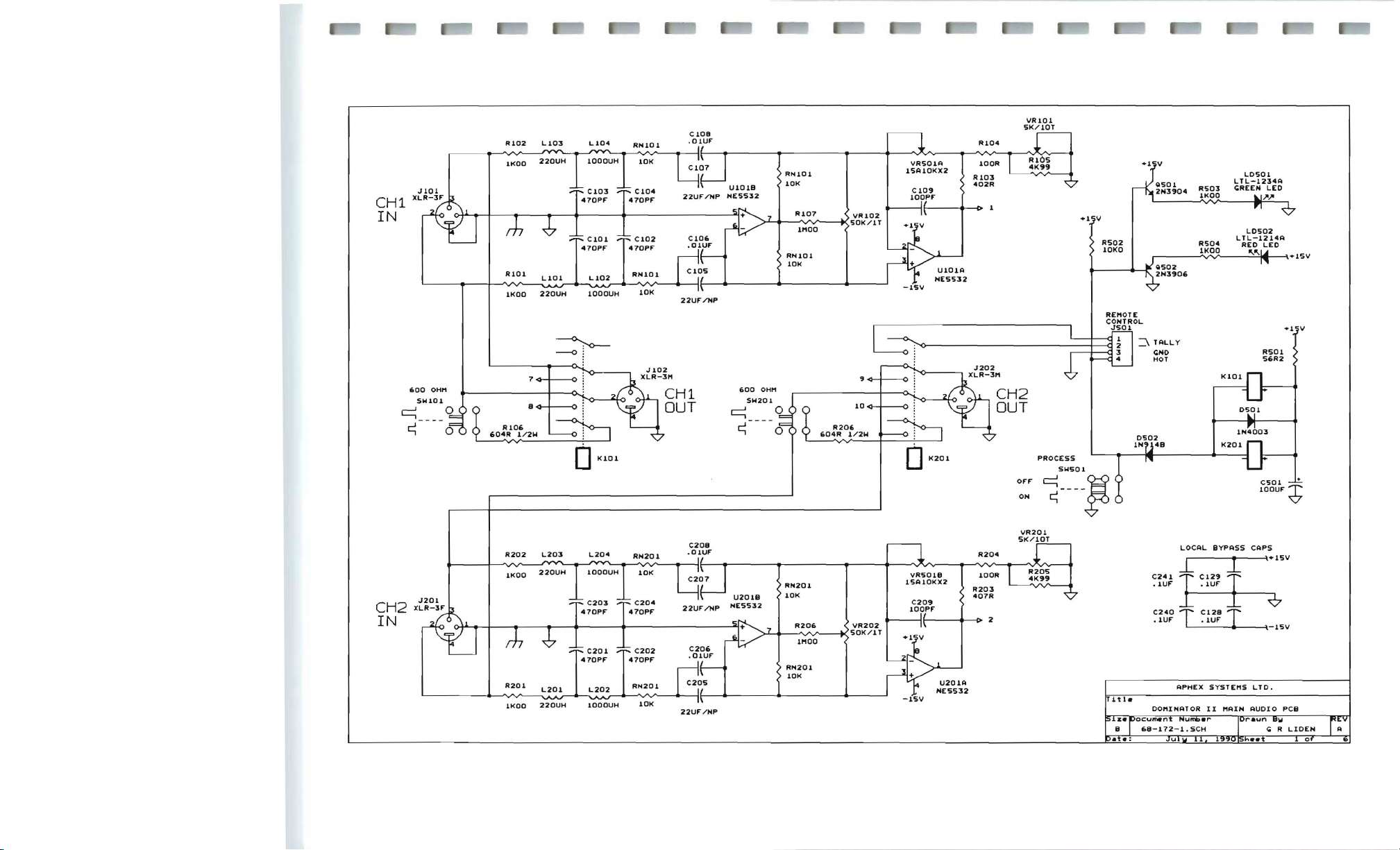
CHi
IN
'"AD
~
~
SWI01
OHM
<i
0
~
RI02
L,03
220UH
IKOO
R,O'
LlO'
u<oo
220UH
7
BE!
R,O'
LID4
lOOOUH
L'02
'OOOUH
~
---<>j
.
o
K'O'
C,OB
RNIOl
'OK
C,02
RNI01
,OK
.OlUF"
VRSCIA
RNIOI
'OK
",07
~5110"/y,2T
11100
RNI01
'OK
ft04R
"20'
9~
'O~
1/2
OHf'1
...
CIOf.
/NP
/NP
UI018
NE5532
600
~
22UF
.0lUF
22UF"
CHi CH2
OUT
~
'5A'OKX2
c,09
'OOPF
1(201
"'00
'00"
R'03
402R
OUT
OFF
VRIOI
51(/
lOT
.1'5\1
"502
'aKa
::\
0502
PROCESS
5W501
~----~
ON
'N9'OB
~
___
TALLY
C::No
HOT
"503
'KOO
"500
~~O
1<201
L050'
LTL-1234A
C::"EEN
LED
7'-"
LD502
LTL-1214A
RED
LED
"''''\4
"50,
5'R2
050,
IH4003
eso
'OOUF
:+'511
+15\1
1 --L!
~
CH2
IN
0)',
IIR20'
C20B
.0lUF
IIR50,8
"N20'
U20'B
NE5532
I
470PF"
R20'
lKOO
LZOI
220UH
L202
lOOOUH
RN201
'OK
22UF"
51_
/HP
'OK
, ~ I
~SOK/IT
"N20'
'OK
,,206
'''00
<.
11"202
'5A,OKX2
C209
'OOPF
R203
007R
R200
'00"
2
5K/'OT
it
1.
iK.pocu~n
B I
68-172-1.
.t.:
LOCAL
...L
C20,
~
APHEX
SCH
C'29
.
lUI'
.
'UF
II
.
lUI'
C200 T CUB
.
'UF
DOMINATOR
BYPASS CAPS
I
~
T
SYSTE"S
LTD.
"'AIN AUDIO PCB
r.un
\+'511
~
'-IS\l
Sw
<;
R
LIDEN
A
Page 71
H503-10
CH'
R,B
10KO
R132
4K')')
Ul020
C040"
U'02C
C040U.
C117
~OPF
R134
6K34
RANGE
LTL-1234A
Jl~JL
-,0
GREEN LEO
o
L0509
-"-"
L05,O
LTL-1214A
REO
LEO
~-"-"
H503-8
RllE.
lOKl
R135
,5KO
Ul028
C040'~
UI02A
4011>
Clla
+'5
1/20PF"
R137
10KO
USIOA
NE5532
RU8
10KO
C1l9
R13')
10KO
+'5
-'5
10PF"
4
3
+ 1 5 V
R507
\---""v"'V"
10KO
Q504
2N3904
~
10KO
+'5~I04
20~lf:-5
0""
H50J-l~.~-~-------------1L--+---------------,
CH2
2
RZ33
10KO
R232
4K99
U202'"
C0401~
U2028
C0401~
SIDE
'----------O~
SoColl1~~
SoC 02"
C217
1/20PF"
R234
6K34
CHAIN
COUPLIN~
SW504
,
,
~~SoC
0---;>50
olL
C 0
2L
~~SoColH
q.--..()
0---;>5
0C0
2H
+15
:ti]
ALTSUI1
~
FINE
VR50~
".''')
DENSITY
VR504
15Al00KX2
R511
lP100
R512
11100
II------i~-~t
+15
CW
r
R236
30Kl
R235
15KO
U202C
CD4016
LS
CH2
CHl
R513
11100
503-5
i;
1 I ill
..
:\
TO
AUX
PCB
H502
r11l
5
~
7
c:l
8
TO
AUX
PCB
H501
n
H503-l
vR505
''',
15Al0K
R505
100R
...
I
I
,:l~:.
U202D
CD4016
DC
SHIFT
+15
TEST 2
~
POWER
+15
~
TEST
H504
SUPPLY
1 t
1.
H505
+,5
R508
'K
18
~
20PF
10KO
U5108
NE5532
NOR""'L
APHEX SYSTEP1S
DOP1INATOR
~
R509
21R5
R239
'OKO
R23B
10KO
TO
U509-7
H50Z-6
R23~/R237
U50~-7
HSOl-4
U50~-1
R
13~/R
137
H502-7
U50')-1
LTD.
II
P1AIN
AUDIO PCB
o R
h
••
CLIPPER
"'503
"
WERRBACH
~
5
PCB
1
2
3
4
53
~
7
B
')
10
I A
Page 72

Page 73
INPUT
<1
TP301
-
SHIFT
-lS
VRlOl
lK
/ l T
....
NULL
1 SHIF"T
"
NULL
R312
2
200K
+1:t
I II
OF"F"SET
10K/ IT
R307
1HOO
Rl04
4K99
VR303
NULL
-lS
....
r----------------------------=--~UT
C302
20P~
R30'>
'>K'O
R31S
10KO
TPl02
+1'>
Rll.
10KO
~(
RlOl
10KO
T£5T<1<1~------------------------;
5.
C.<1--------------------------------------------------------------t------------------,
Rl02
10KO
10P~
Ul018
LF35l
R320
VV'
6K65
R309
21RS
Rl08
~
1KO
U3028
L~353
RlI0
40R2
RlOl
4K'31)
Rll1
40R2
Rl17
101<0
l~~~4
THIS
HOTES :
CIRCUITRY
CHtliHHEL
CHANNEL 2 USES
1 USES
EXISTS 6 Tl"ES
lOO
SERIES
SERIES
PART
PART NUHBERS:
400
UlO48
N£'>532
~
~
______________
Ol03
lN9148
+15
-15
(3
F"OR
CHANNEL
NUHBERS : SUFF"IX
SUFFIX
~
I~
-15
~2~N3'0~
1; l FOR
L=LOW
L=LOW
10KO
Ql02
...,
,
CHANNEL
H=HIO
"="10
U302tli
LF"l53
~HS
R31~
1"'>
"'-/V'
ri
2)
H:HICH
H=HI~H
r
T
ctliLT
---------~£>RLS
1+1SV
~~~:
C305
_ .
L---
1UF'
______
it
i
z.
a I
.ate:
Ie
poc:ulI'Ient
LOCtliL
eYPtliSS
CAPS
_.\-15V
6B-172-4.SCH
APHEX
OOHIHtliTOR
H-urnb.1'"
SYSTEHS
II
"tliIN
LTD .
AUDIO P CB
'"
o R
WERRBACH
A
Page 74

CH
u~oeA
NE5~32
H!!03-7
R127
10KO
R128
10KO
0,02
-j(-
1N~1"'!I
R12.
LOW
1
MID
HIGH
--vv
101<0
10KO
~
~
10KO
~
I
10PF
A1Z6
'VV'
10KO
+1!!V
~
r
-HSV
,.
t
RS.2~
10KO
R130
"'I<~g
Olol
lN91.a
n
R13S.
10KO
+l~V
zJ
-15V
U~08A
LF353
:of
0103
INgl.a
010"
lN91.6
rOO
2-8
CH
R223
LOW
2
MID
HIGH
--vv
10KO
101(0
~
~
101<0
101<0
U~06B
~
NE~~32
H503-.04
R228
10KO
R227
7
10KO
I
~~
u507B
LF303
~
lN9t.04B
~
R229
10KO
R230
.1<951
0201
lN91.B
_sf"l-...
r~
R231
10KO
U~OB8
LF3!!3
f
0203
lNSU4e
020.04
lN91
..
a
Tltl.
slzeloDcum.nt
B
APHEX SYSTEMS
DOHINATOR
Number
eB-172-~ .SCH
LTD.
II
HAIN
AUDIO PCB
Crawn
o R
-By
WERFIBACH
EV
•
Page 75
4<>--1
VRIOS
lOK/l
C124
100UF
RISe
499K
T
R144J
lOKO
'U46
10KO
C127
20PF
RlSO
10KO
·15
J-
A152
10"
C125
.33UF
OUTPUT
BALANCE
lP
01
6<>--1
VR20S
10K/IT
C224
100UF
A258
499K
!
A249
10KO lOKO
R246
10KO
.1!'
-15
RlS4
lQKO
7
RlSS
lOKO
C122
20PF"
R144
332K
I I
~
~
47UH
R147
~
47UH
8
R2SS
lOKO
.15
-15
C227
20PF
A250
R2S4
10KO
U203A
NE5532
R2S1
56R2
A253
332K
R244
332K
U204A
LF353
A252
C225
•
33UF"
U204A
10"
·15
-15
OUTPUT
BALANCE
TP~Ol
A257
20KO
20KO
~
).
R2S6
150R
L206
47UH
47UH
......
9
.15
1
~
R141
10KO
C123
20PF
C131
lOQUF
R142
56R2
-15
1
C130
::&
100UF
C121
.
33uF'
FU43
10"
5
100UF'
<>--1
C219
R240
10KO 10KO
R241
C223
20PF'
(
·15
1
C231
~
100UF
R242
56R2
-15
1
::&
Titl.
c230
100UF'
..
B
..:
Iil
C221
.33UF
R243
10"
-vv
APHEX SYSTEMS
DOMINATOR
ocurn.nt
~e-172-~.SCH
AW
LTD.
II
MAIN AUDIO PCB
o R
••
W
WERRBACH
t
I A
Page 76

4
1
2
3
-lv
J
+lv
16
I I I I I I I I I
+2
0
5
7
9
+4 +6
15 13
+8
+10 +12
-i5
11
10
+14 +16
SIoI1
8 6
+18 +20
12
I I
14
t
~~2
Hl
+15V-
1
+
C2
~22UF
TOTAL
2 3 4 5
-",
-
V V
- +
-15V
150R
C 1 +
22UF
LIMITING
7 8
-.,
' , -
_
8
9
0
A
R3
1KOO
61
~
4
R
L H
6
_I"
I~
I~
6 7
5
5
~
H I
R R R
(dB)
9
I
~~3914
Title
DOMINATOR
sizelDocument
A
6B-176.SCH
IDate
:
10
LD1-10
....
IJIJI
-
APHEX SYSTEMS
II
DISPLAY/SIoIITCH
Number
Ma\::j
21,
1990
LTD.
Draun8y
o R
ISh~et
PCB
IoIERRBACH
1 0
EV
A
1
Page 77

>'1
04
16
15
14
0-
13
v-
12
11
10
9
B
v-
7
6
S
-
30
R2
R1
2491<.
ZERO
R4
RJ
20St<
ZERO
R6
RS
21<.94
3K32
U<02
R12
7S0R
IJJR
R16
249R
442R
402R
1651<.
R7
1331<
R9
110K
Rll
8SI<.7
711<.5
R1S
571<6
R17
4SKJ
R19
36KS
2IJK4
R2J
23K2
RB
Rl0
R14 R13
R18
976R
R20
R22 R21
51R1
R24
+2
+4
+6
+8
:::
+14
+16
+18
+20
+22
+24
TO
R26
49K9
~--f
lfiuF
R25
111<.0
~:.
LF"J47
u+
~rl
SHEET 2
THRESH
R27
lU
nLHJll
f4
10
12
14
16
19
20
22
24
<Q
+lSV
Hl0l
PIN
U1C
LFJ47
OEFINITIONS
rUNeT I ON
CROUND
CROUNO
VR 1
wIPER
VRI
ccw
VR2A
CW/WIPER
VR2A
ccw
vR28
CW/wI
VR28
ccw
PER
RJ9
41<.9"
~~~
;;
,\7
HIO;Z
1876543211
T
Y
TO
07
1N9148
t..II
("II
:::;
C&
.lUF
SHEET 2
~V
_'2
]~
-ISV
I'"
"I
..J
~
L01 ;;;;:
»
C;RN
HI02
PIN
1-
2.
J.
4.
S .
6.
7.
8.
UJA
Lf"347
C9
.OO47UF"
PIN
FUNCTION
c:;;.ROUND
ALI
PHASE
RELEASE
CROUND
CH
1 INPUT
CH2
ALT
~
R72
30Kl
~~~
;;
-ISV
DEFINITIONS
8US
CONTROL
POT
INPUT
RECTIFIER IN
RJ7
41<.99
R3B
10KO
:::::
C10
.OO47Uf"
OB
1N9~14B
?
-,,-
R36
3921<.
~
-ISV
+lS
~
C12
;&.lUF
-lS
~
C13
;&.1UF
010
1N9: 1 4B
-,,-
09
1N~~4B
("II
-
+
U3B
LF347
+lS
~
;&.1U'
-lS
~
;&.lUF
RJS
lOOK
R34
lOOK
C14
C1'i
<
<
VOL T
Ac:;;.E
0.602
0.732
0:893
6
1.100
8
1 .
315
1
1.677
2.094
2 .
60S
3.241
4.060
S.09J
6 .
JSS
+l]V
U2
~
R29
10KO
C6
~OJt'
1\
R74
1KOO
06
1H9148
R28
11KO
RJl
7321<.
~iO:
HIDl
18765
RJO
491<.9
J
r
4
3211
2
RJ2
4K99
Q2
2N3904
..
QJ
J904
PIN
1-
2.
J.
4.
S.
6.
7.
B.
U1B
'-i
{\
. 3 C 3
LF"J47
4::~1~
RlJ
lOOK
~
S
U'
;;!;::
40--\+15
10--\-15
2~
Tit
1.
8
~t.:
DOMINATOR
ocurnent
68-177-1.S
APHEX
SYSTEMS
II
Number
CH D R
AUX
CONTROL PCB
h
LTD.
eet
WERRBACH
1 0
A
Page 78
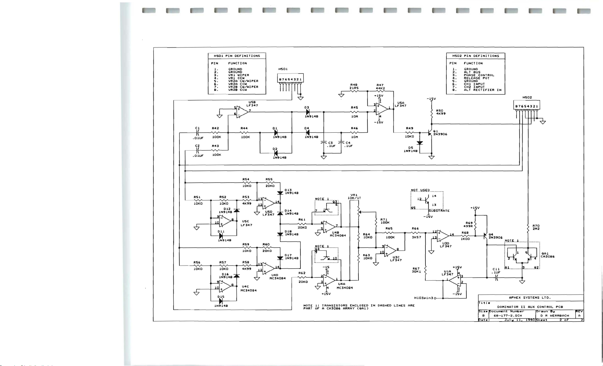
Cl
.0Wf"
cz
.OlUF
H~OI
PIN
2.
3.
~.
S.
6.
7.
B.
R~2
lOOK
R~3
lOOK
1-
PIN
DEFINITIONS
FUNC'ION
<;ROUND
<;ROUND
VRl
IIRl
VR2A
VR2A
VR2& C...
IIR2B
WIPER
CCW
CW.l'WIPER
CCW
.l'WIPER
CCW
R44
lOOK
HSOI
01
~
02
IN-'14&
1
03
~
1N'14&
O~
~
.Wf"
P
R~B
2UIS
.
~
R~6
,
VV
C~
.1Uf"
101<
R~7
:1"
,I.
-l~V
USA
Lf"347
R~9
10KO
05
1N'14a
RSO
~K99
PIN
HS02
1-
2.
3.
4.
5.
i.
7 .
B.
PIN
DEFINITIONS
FUNCTION
<;ROUNO
AL
T BUS
PHASE
CONTROL
RELEASE
<;ROUNO
CH1 INPUT
CH2 INPUT
ALT
RECTIFIER
POT
IN
HS02
R51 R52
10KO
1N914&
*-
RSi
10KO
R57
10K
~
015
lN9148
RS~
10KO
~O
RS3
4K9,
USC
Lf"3~7
R59 R60
10KO
~O
RSB
U~C
t1C3~OB4
RSS
017
1N9148
Ri2
VV'-
20KO
NOTE
PART
10K/1
U~A
I<C340B~
+1'SV
1:
TRANSISTORS ENCLOSEO
OF A CA3086
ARRAY
IIRl
T
(QAl)
Ri4
10KO
Ri3
10KO
IN
R71
lOOK
R6S
lOOK
DASHED
~Q.Li·V·~~r.>
~
~
:9.L
Rii
3KS7
Ri7
30Kl
LINES
ARE
··
~~"
-1511
13
'UEIS'U~'
"·1
~
~
E
U1A
Lf"347
1
.... ....
H103pln30~~--------~
Ri9
499R
+l~V
J.
t
B
..:
04
2"3906
1.
ocumen
68-l77-2.SCH
h··
APHEX
OO"INATOR
u w
...
J.
II
•
R70
21<2
····l
....
··:·
....... ..
9.~.
SYSTE"S
AUX
OAl
CA30Bi
LTD.
CONTROL
PCB
,...un
'"
o R wERRBACH
••
t
A
Page 79
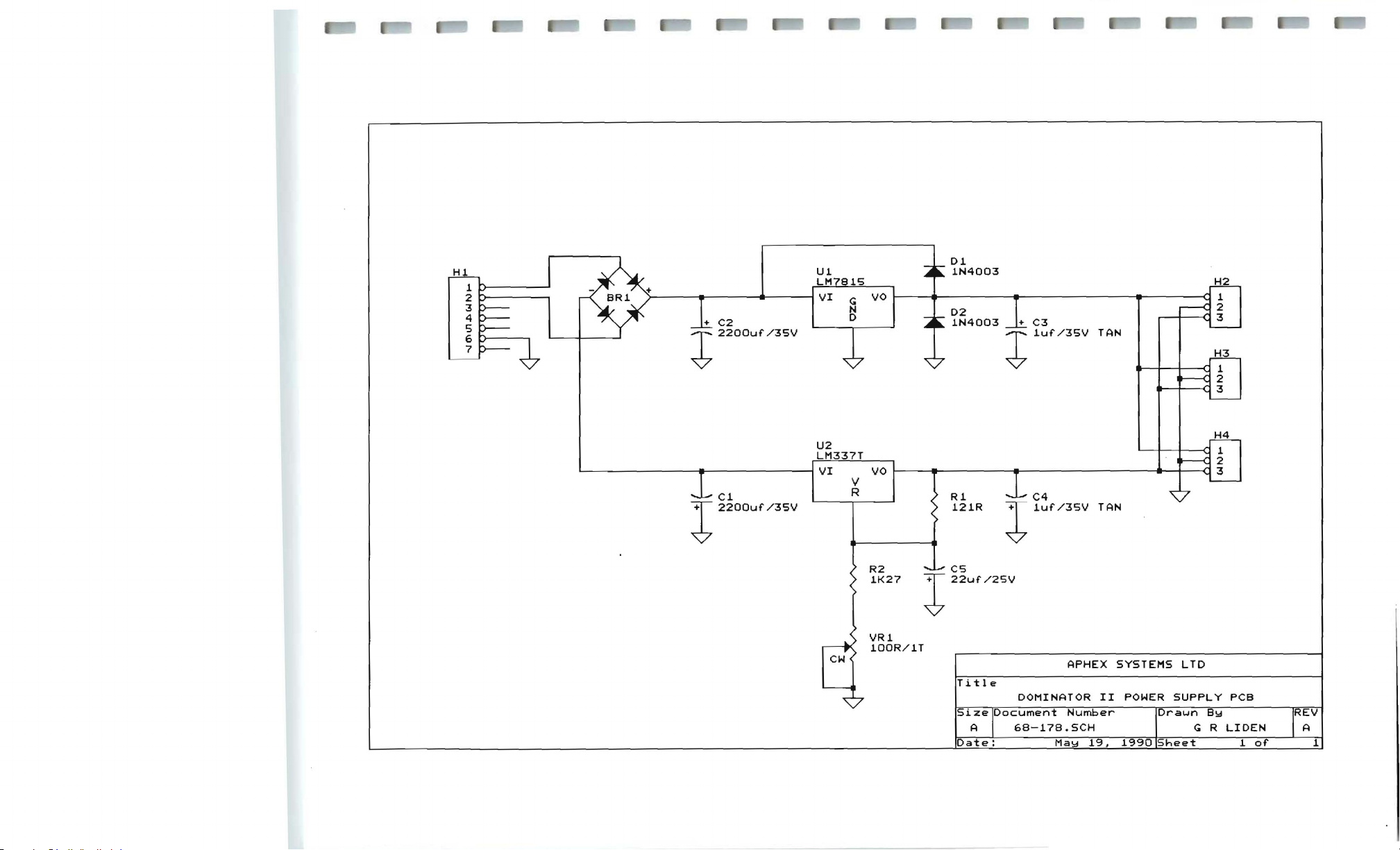
) •
t
+
C2
2200uf
• I
/3SV
U1
LMI9'S
VI
G
~
VO
I
01
1N4003
~
~~4oo31
C3
llUf/3SV
TAN
r
FU
•
d3
H2
1
H3
1
2
•
C1
12200Uf
/3SV
U2
LM331'
I
VI
VO
I ,
V
R 3
R1
121R
R2
1K27
VR1
100R/1
CS
122Uf/2SV
T
Title
5i
Date:
'
l1Uf/3SV
DOMINATOR
zelDocument
A
68-178.SCH
C4
APHEX
Number
May
TAN
SYSTEMS LTD
II
POWER
19.
f990lSheet
1 H4
.
b=ff
2
SUPPLY PCB
Draun
By
G R
LIDEN
1
of
REV
A
1
Page 80

R21
10KO
R22
••
_
~
101(0
.15~U2A
I
-1511
+
_.R~~
10KO
+
U2B
L;353
LF3S3
.1)11
RD
RS
491<9
C2
~1(:,
2N3906
2K49
t I
'~
TO
H503
CH1
AUDIO
CHi
AUOIO
AUDIO
~ROUNO
CLIP
REF"
CH2
AuDIO
CH2 AUDIO
IN
OUT
IN
OUT
·ISV'
eNO
-1511
~
10
9
1
e
Ig~~3~rt
"
S
4
3
2
1
,
I I
~
~
-
~R~1~_t~~~---~
4K99
I
'b
~
Rll
4K99
~(J9PF
R4
10
10KO
R2
41<99
'¢7
I
~
.~~F
R14
10KO
,,,2
41<99
RJ
-IS\I
-IS'"
~
UlA
LFJS3
C7
.1UF
10
H~
12
:............ .....
11
'~
12
1
~
~
10KO
R1S
49K9
t:
/l
lS
I
li
..LJ.
C5
20PF
~~
Qz
CiAJ096E
i:i
...
i·······U·················
9
~
7
f
20~F
R9
2K49
-15v
.1)11
R1D
21<49
.....2...............................
I~
~
,li~
R19
2K49
-ISV'
R17
VV'
10KO
6
Rl0
491<9
..............
R20
49K9
Titl.
1
.....:
DOHINATOR
L.IE_
[OCUw.ntNUIf't:I.r
B
68-179.
at.:
APHEX
II
PROCRAMMABLE
SCH
H.
SYSTEHS
LTD.
CLIPPER
r •
...,n
aw
o R WERRBACH
PCB
Page 81

TO
HSOJ
CHl
AUDIO
AUDIO
<;ROUND
CLIP
REF
CH2 AUDIO
IN
IN
10
9
7
e
6
;
2
1
~
vv
Rl
4P<9;
R21
10KO
~(
R4
lOKO lOKO
t I
:~99
R3
3
-isli
19PF
U28
~
lOKO
RS
49K9
+115\1
C2
20PF
~(
-1$"
+15\1
R6
2K49
I~
20~F
R9
2K.9
~
~
R10
49K'J
+lSV
eND
-lSII
Rll
.K99
lOKO
R12
4K'J9
R14
.
C7
1UF
R16
-115\1
2P<49
R17
1~
itle
DOMINATOR
z-rocument
B
.t.
:
APHEX
II
Numbel""
6B-1BO-l.SCH
K.
SYSTE"S
CLIPPER + PRE/OE-£MP
LTD.
I""AUn
D R
h.et
Bow
WERRBACH
PCB
..
CS
R1S
49K9
B
~(
¢ I
20PF
Page 82
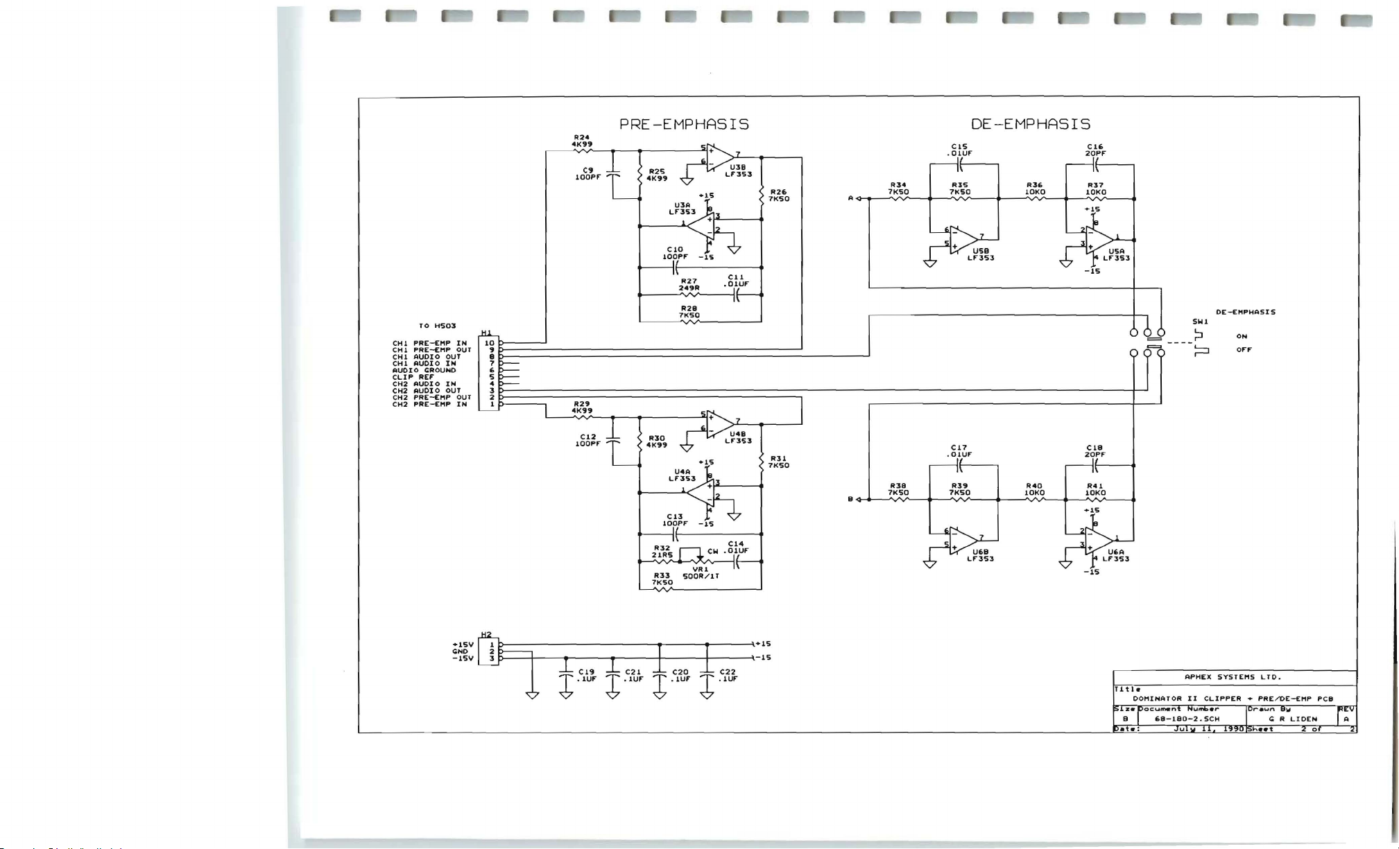
R24
4t(99
C~
100P~
PRE-EMPHASIS
R25
4K99
+15
R2~
?K50
DE-EMPHASIS
C15
.OlU~
R34
?K50
A4-~~vv~~~~rv~--+---~~--~--~~--~
Cl~
20P~
R37
10KO
+15
TO
CHI
PRE-£"P
CHI
PRE-E"P
CHI AUDIO
CHl
AUDIO
AUOIO
CROUNO
CLIP
R[~
CH2
AUDIO
CH2
PR[-E~P
CH2
AuDIO
CH2
pRE-E"P
H503
OUT
IN
IN
OUT
R2?
249R
R28
?K50
our
9·
IN
IOg~::::::~::::::::::::::::::::::::::::::::::::::::::::::~
e
?
~
5
4
OUT
2
3~:::::::~::::;;;=::::::::::::::::::::::::::::::::::::::~----------~==============================================:j~
IN
+15"1
C:NO
-15'"
I
p
tl>--i--r---T--+---+-------
R29
4K~9
C12
100PF"
R30
4K99
R32
21R$
R33
7K50
C13
100PF"
+15
-15
,+15
t
-
15
R31
7K50
__________
J
C17
.
OlUF"
R38 R39
7K50
B~~--~V---~--~~~--~----~~--~--JV~----~
7K50
R40
IOKO
-15
C18
20PF"
R41
lOKO
+15
-15
~1tl.
DO"INArOR
Z-Focum.nt
a
.t.:
5"1
~
~
APHEX
II
CLIPPER +
Number
~e-laO-2.scH
OE-E"PHASI$
ON
O~~
$YSrE"S
LTD.
PRE/DE-E"P
r
.....n ew
••
(;;;
R LIDEN
i
pea
"
 Loading...