

Apex Microtechnology Corporation EB03 Datasheet
TRIPLE INDEPENDENT LOGIC INTERFACED HALF BRIDGES
MICROTECHNOLOGY
HTTP://WWW.APEXMICROTECH.COM (800) 546-APEX (800) 546-2739
FEATURES
• COMPATIBLE WITH PWM FREQUENCIES UP TO 50KHZ
• 10V TO 200V MOTOR SUPPLY
• 5A CONTINUOUS OUTPUT CURRENT
• HCMOS COMPATIBLE SCHMITT TRIGGER LOGIC INPUTS
• SEPARATE SOURCE OUTPUTS FOR NEGATIVE RAIL
CURRENT SENSE
• SLEEP MODE
• WIDE RANGE FOR GATE DRIVE AND LOGIC SUPPLIES
APPLICATIONS
HIGH POWER CIRCUITS FOR DIGITAL CONTROL OF:
• THREE AXIS MOTION USING BRUSH TYPE MOTORS
• THREE PHASE BRUSHLESS DC MOTOR DRIVE
• THREE PHASE AC MOTOR DRIVE
• THREE PHASE HIGH POWER MICROSTEPPING STEP
MOTORS
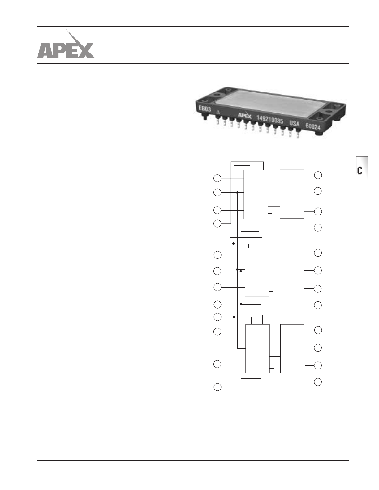
EBO3
12
Hin 1
SD
11
Lin 1
10
Half
Bridge
Driver
FET
Half
Bridge
Output
13
14
15
HV1
OUT1
S1
DESCRIPTION
The EB03 consists of three independent FET half
bridges with drivers. The drivers may be interfaced with
CMOS or HCMOS level logic.
V
,Logic Ground
ss
V
,Logic Supply
dd
V 1
cc
Hin 2
Lin2
V 2
cc
Hin3
Lin 3
V 3
cc
9
8
Half
7
6
5
4
3
2
1
Bridge
Driver
Half
Bridge
Driver
FET
Half
Bridge
Output
FET
Half
Bridge
Output
16
17
18
19
20
21
22
23
24
HVRTN1
HV2
OUT2
S2
HVRTN2
HV3
OUT3
S3
HVRTN3
FIGURE 1. BLOCK DIAGRAM
APEX MICROTECHNOLOGY CORPORATION • TELEPHONE (520) 690-8600 • FAX (520) 888-3329 • ORDERS (520) 690-8601 • EMAIL prodlit@apexmicrotech.com
1

EB03
ABSOLUTE MAXIMUM RATINGS
SPECIFICATIONS
ABSOLUTE MAXIMUM RATINGS
MOTOR VOLTAGE SUPPLY, HV 200V
OUTPUT CURRENT, peak 10A
OUTPUT CURRENT, continuous1 5A
GATE SUPPLY VOLTAGE, Vcc 20V
LOGIC SUPPLY VOLTAGE, Vdd 20V
POWER DISSIPATION, internal1 40W
LOGIC INPUT VOLTAGE -0.3V to Vdd + 0.3V
THERMAL RESISTANCE TO CASE3 2.1°C/Watt
TEMPERATURE, pin solder, 10s 300°C
TEMPERATURE, junction2 150°C
TEMPERATURE RANGE, storage –55 to +150°C
OPERATING TEMPERATURE, case –25 to +85°C
SPECIFICATIONS
PARAMETER TEST CONDITIONS MIN TYP MAX UNITS
POSITIVE OUTPUT VOLTAGE I
HV=100V, Fpwm=50kHz, L=100 µH
NEGATIVE OUTPUT VOLTAGE " -1.7 1.9 Volts
POSITIVE EDGE DELAY " 310 n-second
RISETIME " 50 n-second
NEGATIVE EDGE DELAY " 290 n-second
FALLTIME " 50 n-second
PWM FREQUENCY Set by external circuitry 50 kHz
INPUT IMPEDANCE Set by internal resistors 50 k-ohm
INPUT AND OUTPUT SIGNALS
PIN SYMBOL FUNCTION PIN SYMBOL FUNCTION
1 V
2 Lin3 Low drive logic in 3 14 OUT1 Section 1 output
3 Hin3 High drive logic in 3 15 S1 Section 1 source
4 V
5 V
6 Lin2 Low drive logic in 2 18 OUT 2 Section 2 output
7 V
8 Hin2 High drive logic in 2 20 HVRTN2 Section 2 return
9 V
10 Lin1 Low drive logic in 1 22 OUT 3 Section 3 output
11 SD Shut down logic in 23 S3 Section 3 source
12 Hin1 High drive logic in 1 24 HVRTN 3 Section 3 return
3 Gate supply 3 13 HV1 High Voltage supply 1
cc
Logic supply 16 HVRTN1 Section 1 return
dd
2 Gate supply 2 17 HV2 High voltage supply 2
cc
Signal ground 19 S2 Section 2 source
ss
1 Gate supply 1 21 HV3 High voltage supply 3
cc
=5A; Vcc=10.8V , Vdd=5V; 198.1 201.9 Volts
OUT
NOTES: 1. Over Entire Environmental Range.
2. Long term operation at the maximum junction temperature will result in reduced product life. Lower internal temperature by
reducing internal dissipation or using better heatsinking to achieve high MTTF.
3. Each FET.
INPUT
A logic level input independently controls each FET in
the half bridge. A logic level high turns on the FET and
However, input impedance is 50k on all inputs; therefore if
one input is open circuited a high radiated noise level could
spuriously turn on a FET.
low turns it off. A common shut down input turns off all
FETs when high.
All inputs are Schmitt triggers with the upper threshold at
and the lower threshold at 1/3 Vdd. This comfortably
2/3 V
dd
interfaces with CMOS or HCMOS provided that the Vdd for
the logic family and the EB03 are the same.
TTL families may be used if a pull-up to Vcc is added to
the TTL gates driving the EB03, and Vdd for the EB03 is the
same supply as V
An open signal connector pulls the shut down input high
for the TTL family.
cc
OUTPUT
Each output section consists of a switching mode FET half
bridge. Separate HV supply, emitter, and HV return lines are
provided for each section.
The FETs are conservatively rated to carry 5A. At 5A the
saturation voltage is 1.9V maximum.
Each FET has an intrinsic diode connected in anti-parallel.
When switching an inductive load this diode will conduct, and
the drop at 5A will be 1.9V maximum.
and all other inputs low, insuring that all outputs are off.
APEX MICROTECHNOLOGY CORPORATION • 5980 NORTH SHANNON ROAD • TUCSON, ARIZONA 85741 • USA • APPLICATIONS HOTLINE: 1 (800) 546-2739
2
 Loading...