

HIGH VOLTAGE POWER OPERATIONAL AMPLIFIER
MICROTECHNOLOGY
HTTP://WWW.APEXMICROTECH.COM (800) 546-APEX (800) 546-2739
FEATURES
• HIGH VOLTAGE — 450V (±225V)
• HIGH SLEW RATE — 1000V/µS
• HIGH OUTPUT CURRENT — 200mA
APPLICATIONS
• HIGH VOLTAGE INSTRUMENTATION
• PIEZO TRANSDUCER EXCITATION
• PROGRAMMABLE POWER SUPPLIES UP TO 430V
• ELECTROSTATIC TRANSDUCERS & DEFLECTION
PA98
PATENTED
DESCRIPTION
The PA98 is a high voltage, high power bandwidth MOSFET
operational amplifier designed for output currents up to 200mA.
Output voltages can swing up to ±215V with a dual supply and
up to +440 volts with a single supply. The safe operating area
(SOA) has no second breakdown limitations and can be
observed with all types of loads by choosing an appropriate
current limiting resistor. High accuracy is achieved with a
cascode input circuit configuration. All internal biasing is
referenced to a bootstrapped zener-MOSFET current source.
As a result, the PA98 features an unprecedented supply range
and excellent supply rejection. The MOSFET output stage is
biased on for linear operation. External compensation provides user flexibility.
This hybrid circuit utilizes thick film (cermet) resistors, ceramic capacitors and silicon semiconductor chips to maximize
reliability, minimize size and give top performance. Ultrasonically bonded aluminum wires provide reliable interconnections at all operating temperatures.
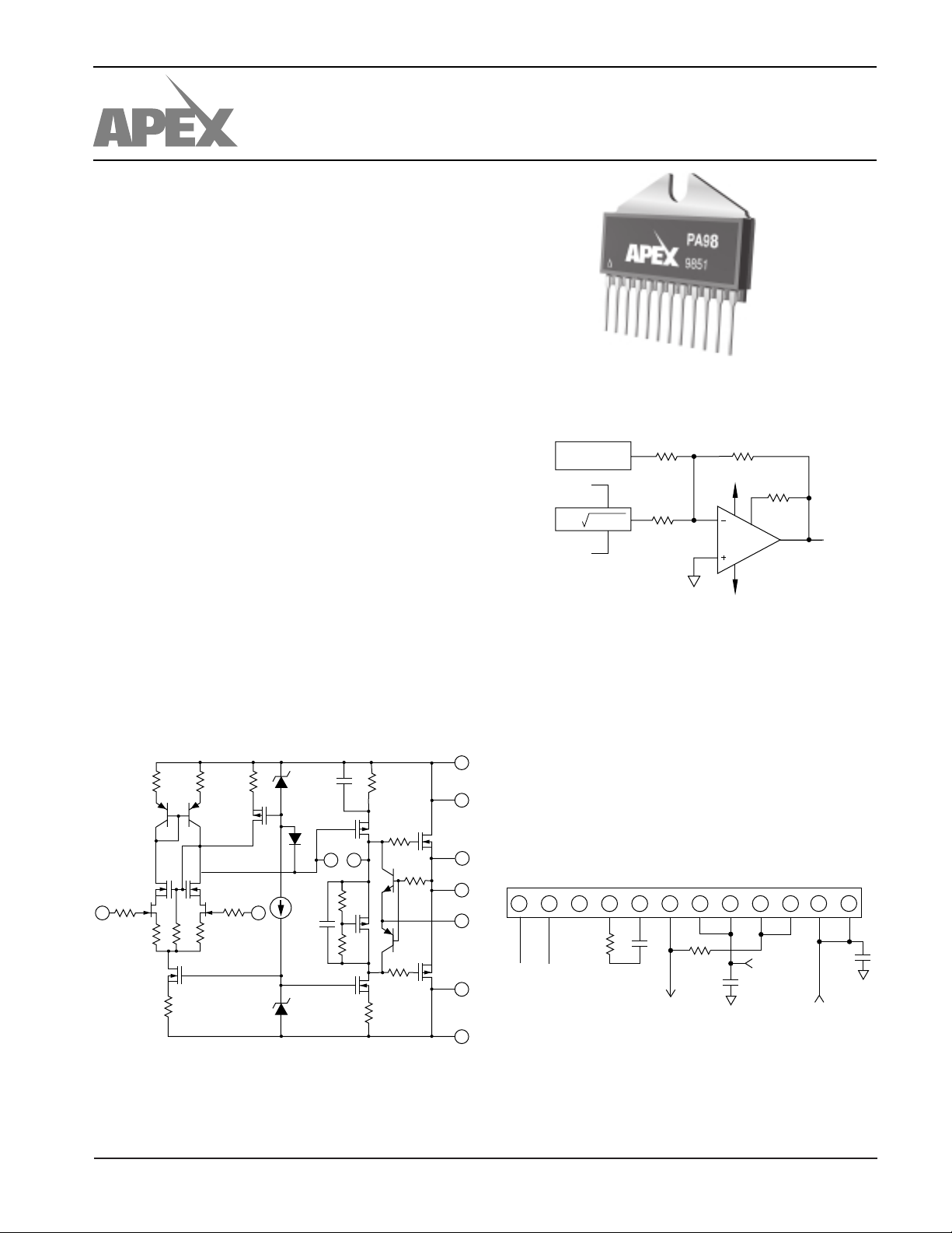
EQUIVALENT SCHEMATIC
D1
Q10B
Q4
21
D2
D23
COMP
54
Q11
Q8
Q16
Q9
Q12
OUT
Q17
Q18
Q1 Q2
Q6 Q7
–IN +IN
Q10A
Q13
11
+V
12
+V
10
–V
–V
TYPICAL APPLICATION
R
IN1
R
IN2
FOCUS
X SWEEP
SAMPLE
z = x + y
Y SWEEP
SAMPLE
DC
2
2
DYNAMIC FOCUSING
Dynamic focusing is the active correction of focusing voltage as a beam traverses the face of a CRT. This is necessary
in high resolution flat face monitors since the distance between cathode and screen varies as the beam moves from the
center of the screen to the edges. PA98 lends itself well to this
function since it can be connected as a summing amplifier with
inputs from the nominal focus potential and the dynamic
correction. The nominal might be derived from a potentiometer, or perhaps automatic focusing circuitry might be used to
S
generate this potential. The dynamic correction is generated
from the sweep voltages by calculating the distance of the
S
beam from the center of the display.
9
C
C
6
8
7
EXTERNAL CONNECTIONS PACKAGE: SIP03
L
L
S
S
12345678910
NC
R
c
–IN +IN
PHASE COMPENSATION
Gain C
1 68pF 100Ω
20 10pF 330Ω
100 3.3pF 0Ω
CC RATED FOR FULL SUPPLY VOLTAGE
C
c
TO LOAD
AND FEEDBACK
C
R
C
R
F
+225V
PA98
±225V
R
CL
–V
*
* Bypassing required.
R
CL
TO
FOCUS
GRID
11
12
*
s
+V
s
APEX MICROTECHNOLOGY CORPORATION • TELEPHONE (520) 690-8600 • FAX (520) 888-3329 • ORDERS (520) 690-8601 • EMAIL prodlit@apexmicrotech.com
PA98
ABSOLUTE MAXIMUM RATINGS
SPECIFICATIONS
ABSOLUTE MAXIMUM RATINGS
SUPPLY VOLTAGE, +VS to –V
OUTPUT CURRENT, continuous within SOA 200mA
S
450V
POWER DISSIPATION, continuous @ TC = 25°C230W
INPUT VOLTAGE, differential ±25V
INPUT VOLTAGE, common mode ±V
TEMPERATURE, pin solder - 10s max 220°C
TEMPERATURE, junction
2
S
150°C
TEMPERATURE, storage –65 to +150°C
OPERATING TEMPERATURE RANGE, case –55 to +125°C
SPECIFICATIONS
PARAMETER TEST CONDITIONS
INPUT
OFFSET VOLTAGE, initial .5 2 mV
OFFSET VOLTAGE, vs. temperature Full temperature range 10 30 µV/°C
OFFSET VOLTAGE, vs. supply 3 10 µV/V
OFFSET VOLTAGE, vs. time 75 µV/√kh
BIAS CURRENT, initial
BIAS CURRENT, vs. supply .01 pA/V
OFFSET CURRENT, initial
3
3
INPUT IMPEDANCE, DC 10
INPUT CAPACITANCE 4pF
COMMON MODE VOLTAGE RANGE
4
COMMON MODE REJECTION, DC VCM = ±90V 90 110 dB
NOISE 100kHz BW, RS = 1KΩ, CC = 10pf 1 µVrms
GAIN
OPEN LOOP, @ 15Hz RL = 2KΩ, CC = OPEN 96 111 dB
GAIN BANDWIDTH PRODUCT at 1MHz RL = 2KΩ, CC = 3.3pf 100 MHz
POWER BANDWIDTH CC = 10pf 300 kHz
CC = 3.3pf 500 kHz
PHASE MARGIN Full temperature range 60 °
OUTPUT
VOLTAGE SWING
VOLTAGE SWING
VOLTAGE SWING
4
4
4
IO = ±200mA ±Vs–10 ±Vs–6.5 V
IO = ±75mA ±V–8.5 ±Vs–6.0 V
IO = ±20mA ±V–8.0 ±Vs–5.5 V
CURRENT, continuous TC = 85°C ±200 mA
SLEW RATE, AV = 20 CC = 10pf 400 V/µs
SLEW RATE, AV = 100 CC = OPEN 1000 V/µs
CAPACITIVE LOAD, AV = +1 Full temperature range 470 pf
SETTLING TIME to .1% CC = 10pf, 2V step 1 µs
RESISTANCE, no load RCL = 0 50 Ω
POWER SUPPLY
VOLTAGE
6
Full temperature range ±15 ±150 ±225 V
CURRENT, quiescent 21 25 mA
THERMAL
RESISTANCE, AC, junction to case
5
Full temperature range, F > 60Hz 2.5 °C/W
RESISTANCE, DC, junction to case Full temperature range, F < 60Hz 4.2 °C/W
RESISTANCE, junction to air Full temperature range 30 C/W
TEMPERATURE RANGE, case Meets full range specifications –25 +85 °C
1
MIN TYP MAX UNITS
550pA
10 100 pA
11
Ω
±VS–12 V
NOTES: 1. Unless otherwise noted: TC = 25°C, compensation = CC = 68pF, RC = 100Ω. DC input specifications are ± value given. Power
supply voltage is typical rating.
2. Long term operation at the maximum junction temperature will result in reduced product life. Derate internal power dissipation
to achieve high MTTF. Ratings apply only to output transistors. An additional 10W may be dissipated due to quiescent power.
3. Doubles for every 10°C of temperature increase.
4. +VS and –VS denote the positive and negative power supply rail respectively.
5. Rating applies if the output current alternates between both output transistors at a rate faster than 60Hz.
6. Derate max supply rating .625 V/°C below 25°C case. No derating needed above 25°C case.
CAUTION
The PA98 is constructed from MOSFET transistors. ESD handling procedures must be observed.
The internal substrate contains beryllia (BeO). Do not break the seal. If accidentally broken, do not crush, machine, or
subject to temperatures in excess of 850°C to avoid generating toxic fumes.
APEX MICROTECHNOLOGY CORPORATION • 5980 NORTH SHANNON ROAD • TUCSON, ARIZONA 85741 • USA • APPLICATIONS HOTLINE: 1 (800) 546-2739

TYPICAL PERFORMANCE
GRAPHS
PA98
40
POWER DERATING
32
24
16
OUTPUT STAGE
8
0
0 25 50 75 100 125 150
INTERNAL POWER DISSIPATION, P(W)
CASE TEMPERATURE, T (°C)
SMALL SIGNAL RESPONSE
120
C
100
C = 3.3pF
80
60
C = 10pF
C
C
40
20
C = 68pF
0
OPEN LOOP GAIN, A (dB)
–20
10
100 1K 10K .1M 1M
C
FREQUENCY, F (Hz)
10M
20M
PHASE RESPONSE
0
–45
–90
Φ
–135
PHASE, (°)
–180
–225
–270
.2M
10
SO
9
8
7
6
5
4
0
VOLTAGE DROP FROM SUPPLY, V – V (V)
1M 10M 40M
FREQUENCY F (Hz)
OUTPUT VOLTAGE SWING
100
OUTPUT CURRENT, I (mA)
C = 68pF
C
C = 10pF
C = 3.3pF
C
C
T = 125°C
T = 25
C
T = –55°C
C
C
°C
O
200
250
Q
1.20
QUIESCENT CURRENT
1.15
1.10
1.05
1.00
C
T = 125
T = 25°C
C
T =
C
°C
–55°C
.95
.90
0 100 300 400
TOTAL SUPPLY VOLTAGE, V (V)
NORMALIZED QUIESCENT CURRENT, I (X)
200
450
S
POWER RESPONSE
500
PP
250
O
125
100
C = 68pf
C
75
50
R = 2K Ω
OUTPUT VOLTAGE, V (V )
L
25
FREQUENCY, F (Hz)
C = 10pf
C
500K
C = 3.3pf
C
1M
5M
2M50K 100K 200K
1000
SLEW RATE
µ
500
200
SLEW RATE, (V/ S)
100
060
EXT. COMPENSATION CAPACITOR, C (pF)
COMMON MODE REJECTION
140
120
100
80
60
40
20
1K 10K 10M
COMMON MODE REJECTION, CMR (dB)
30 75
C = 10pF
C
100K 1M
FREQUENCY, F (Hz)
9015 45 10
C
HARMONIC DISTORTION
.05
AV = 30
.03
P = 15W
O
C = 10pf
C
R = 1KΩ
L
.01
.005
.003
DISTORTION, (%)
INPUT NOISE VOLTAGE
20
÷
15
N
10
7
5
3
.001
FREQUENCY, F (Hz)
100K100 1K 10K
2
INPUT NOISE VOLTAGE, V (nV/ Hz)
10 100 10K 100K
FREQUENCY, F (Hz)
POWER SUPPLY REJECTION
140
120
100
80
60
40
20
10 100 1K 10K .1M
11M
POWER SUPPLY REJECTION, PSR (dB)
FREQUENCY, F (Hz)
500
300
200
LIM
100
50
CURRENT LIMIT, I (mA)
20
1 5 10 30
220
RESISTOR VALUE, R ( )
1K
CURRENT LIMIT
Ω
CL
APEX MICROTECHNOLOGY CORPORATION • TELEPHONE (520) 690-8600 • FAX (520) 888-3329 • ORDERS (520) 690-8601 • EMAIL prodlit@apexmicrotech.com

PA98
GENERAL
Please read the “General Operating Considerations” section, which covers stability, supplies, heatsinking, mounting,
current limit, SOA interpretation, and specification interpretation. Additional information can be found in the application
notes. For information on the package outline, heatsinks, and
mounting hardware, consult the “Accessory and Package
Mechanical Data” section of the handbook.
CURRENT LIMIT
For proper operation, the current limit resistor (RCL) must be
connected as shown in the external connection diagram. The
minimum value is 1.4 ohm, however for optimum reliability the
resistor value should be set as high as possible. The value is
calculated as follows; with the maximum practical value of 30
ohms.
R
CL
SAFE OPERATING AREA (SOA)
The MOSFET output stage of this power operational amplifier has two distinct limitations:
1. The current handling capability of the MOSFET geometry
and the wire bonds.
2. The junction temperature of the output MOSFETs.
NOTE: The output stage is protected against transient flyback.
However, for protection against sustained, high energy flyback,
external fast-recovery diodes should be used.
SAFE OPERATING CURVES
The safe operating area curves define the maximum additional internal power dissipation the amplifier can tolerate
when it produces the necessary output to drive an external
load. This is not the same as the absolute maximum internal
500
300
, (mA)
S
200
OR –V
S
100
50
30
20
=
DC, T
I
LIM
.7
- .016
200mS
C
= 125
DC, T
°C
DC, T
C
= 85
C
°C
= 25
100mS
°C
OPERATING
CONSIDERATIONS
power dissipation listed elsewhere in the specification since
the quiescent power dissipation is significant compared to the
total.
INPUT PROTECTION
Although the PA98 can withstand differential voltages up to
±25V, additional external protection is recommended. Since
the PA98 is a high speed amplifier, low leakage, low capacitance JFETs connected as diodes are recommended (e.g.
2N4416, Q1-Q4 in Figure 1). The differential input voltage will
be clamped to ±1.4V. This is sufficient overdrive to produce
maximum power bandwidth.
POWER SUPPLY PROTECTION
Unidirectional zener diode transient suppressors are recommended as protection on the supply pins. The zeners clamp
transients to voltages within the power supply rating and also
clamp power supply reversals to ground. Whether the zeners
are used or not, the system power supply should be evaluated
for transient performance including power-on overshoot and
power-off polarity reversals as well as line regulation.
Conditions which can cause open circuits or polarity reversals on either power supply rail should be avoided or protected
against. Reversals or opens on the negative supply rail is
known to induce input stage failure. Unidirectional transzorbs
prevent this, and it is desirable that they be both electrically and
physically as close to the amplifier as possible.
STABILITY
The PA98 is externally compensated and performance can
be tailored to the application. Use the graphs of small signal
response and power response as a guide. The compensation
capacitor C
capacitor is recommended. The compensation network C
must be mounted closely to the amplifier pins 7 and 8 to avoid
spurious oscillation.
–IN
Q1
Q2
+IN
FIGURE 1.
OVERVOLTAGE
PROTECTION
must be rated at 500V working voltage. An NPO
C
+V
S
Z1
1
11, 12
Q3
Q4
PA98
7, 8
2
–V
S
6
Z2
CRC
OUTPUT CURRENT FROM +V
PULSE CURVES @ 10% DUTY CYCLE MAX
10
25 50 75 100 250 500
SUPPLY TO OUTPUT DIFFERENTIAL, VS –VO (V)
This data sheet has been carefully checked and is believed to be reliable, however, no responsibility is assumed for possible inaccuracies or omissions. All specifications are subject to change without notice.
APEX MICROTECHNOLOGY CORPORATION • 5980 NORTH SHANNON ROAD • TUCSON, ARIZONA 85741 • USA • APPLICATIONS HOTLINE: 1 (800) 546-2739
125
PA98U REV.A OCTOBER 1999 © 1999 Apex Microtechnology Corp.
 Loading...