

Page 1
HIGH VOLTAGE POWER OPERATIONAL AMPLIFIER
F
R
PA97
IN
R
PIEZO DRIVE
S
–V
S
+V
OUT
V
COMPUTER
FOCUS
COMMAND
VOLTAGE
MICROTECHNOLOGY
HTTP://WWW.APEXMICROTECH.COM (800) 546-APEX (800) 546-2739
FEATURES
• HIGH VOLTAGE — 900V (±450V)
• LOW QUIESCENT CURRENT — 600µA
• HIGH OUTPUT CURRENT — 10mA
APPLICATIONS
• MASS SPECTROMETERS
• SCANNING COILS
• HIGH VOLTAGE INSTRUMENTATION
• PROGRAMMABLE POWER SUPPLIES UP TO 880V
• SEMICONDUCTOR MEASUREMENT EQUIPMENT
PA97
PATENT PENDING
DESCRIPTION
The PA97 is a high voltage MOSFET operational amplifier
designed as a low cost solution for driving continuous output
currents up to 10mA and pulse currents to 15mA into capacitive loads. The safe operating area (SOA) has no second
breakdown limitations. The MOSFET output stage is biased
class C for low quiescent current operation. External compensation provides flexibility in choosing bandwidth and slew rate
for the application. APEX’s SIP05 package uses a minimum of
board space allowing for high density circuit boards.
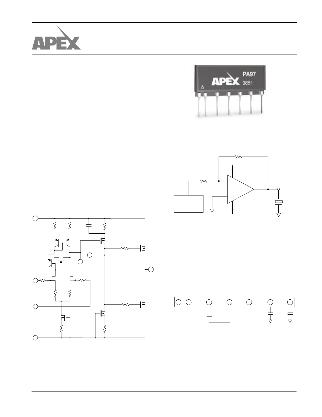
EQUIVALENT SCHEMATIC
12
+V
S
1
–IN
2
+IN
R1 R2 C1 R3
Q1 Q2
Q6
Q5
Q6
R5
R7 R8
Q8
CC1
4
Q7
R6
6
CC2
Q3
Q9
R4
R9
Q4
8
OUT
Q10
TYPICAL APPLICATION
LOW POWER, PIEZOELECTRIC POSITIONING
Piezo positioning may be applied to the focusing of segmented mirror systems. The composite mirror may be composed of hundreds of elements, each requiring focusing under
computer control. In such complex systems the PA97 reduces
the costs of power supplies and cooling with its advantages of
low cost and low quiescent power consumption while increasing circuit density with the SIP package.
EXTERNAL CONNECTIONS PACKAGE: SIP05
–IN +IN CC1 CC2 OUT –Vs +Vs
12 4 6 8 10
*
C
c
**
12
–V
10
APEX MICROTECHNOLOGY CORPORATION • TELEPHONE (520) 690-8600 • FAX (520) 888-3329 • ORDERS (520) 690-8601 • EMAIL prodlit@apexmicrotech.com
R10 R11
S
*
.01µF or greater ceramic power supply bypassing required.
Cc =10pF minimum, 1kV NPO(COG)
PHASE COMPENSATION
GAIN
≥
10 10pF
C
C
Page 2
PA97
ABSOLUTE MAXIMUM RATINGS
SPECIFICATIONS
ABSOLUTE MAXIMUM RATINGS
SUPPLY VOLTAGE, +VS to –V
OUTPUT CURRENT, source, sink 15mA, within SOA
POWER DISSIPATION, continuous @ TC = 25°C5W
INPUT VOLTAGE, differential
S
3
INPUT VOLTAGE, common mode (See Text) ±V
TEMPERATURE, pin solder - 10s max 220°C
TEMPERATURE, junction
2
900V
±20V
S
150°C
TEMPERATURE, storage –65 to +150°C
OPERATING TEMPERATURE RANGE, case –55 to +125°C
SPECIFICATIONS
PARAMETER TEST CONDITIONS
INPUT
OFFSET VOLTAGE, initial .5 5 mV
OFFSET VOLTAGE, vs. temperature Full temperature range 10 50 µV/°C
OFFSET VOLTAGE, vs. supply 10 25 µV/V
OFFSET VOLTAGE, vs. time 75 µV/√kh
BIAS CURRENT, initial 200 2000 pA
BIAS CURRENT, vs. supply 4 pA/V
OFFSET CURRENT, initial 50 500 pA
INPUT IMPEDANCE, DC 10
INPUT CAPACITANCE 4pF
COMMON MODE VOLTAGE RANGE3VS=±250V See Note 3 ±VS 30 V
COMMON MODE REJECTION, DC VCM = ±90V 80 98 dB
NOISE 10KHz BW, RS = 1KΩ, CC = 10pF 2 µVrms
GAIN
OPEN LOOP, @ 15Hz RL = 5KΩ, CC = 10pF 94 111 dB
GAIN BANDWIDTH PRODUCT at 1MHz RL = 5KΩ, CC = 10pF 1 MHz
POWER BANDWIDTH RL = 5KΩ, CC = 10pF 2 kHz
PHASE MARGIN, AV = 100 Full temperature range 60 °
OUTPUT
VOLTAGE SWING
3
IO = 10mA ±VS 24 ±VS 20 V
CURRENT, continuous 10 mA
SLEW RATE, AV = 100 CC = 10pF 8 V/µs
SETTLING TIME to .1% CC = 10pF, 2V step 2 µs
RESISTANCE 10mA Load 100 Ω
POWER SUPPLY
VOLTAGE
5
See note 5 ±50 ±300 ±450 V
CURRENT, quiescent, .6 1 mA
THERMAL
RESISTANCE, AC, junction to case
4
Full temperature range, F > 60Hz 20 °C/W
RESISTANCE, DC, junction to case Full temperature range, F < 60Hz 25 °C/W
RESISTANCE, junction to air Full temperature range 40 °C/W
TEMPERATURE RANGE, case –25 +85 °C
1
MIN TYP MAX UNITS
11
Ω
±
±
±
NOTES: 1. Unless otherwise noted: TC = 25°C, DC input specifications are ± value given. Power supply voltage is typical rating.
CC = 10pF.
2. Long term operation at the maximum junction temperature will result in reduced product life. Derate internal power dissipation
to achieve high MTTF.
3. Although supply voltages can range up to ± 450V the input pins cannot swing over this range. The input pins must be at least
30V from either supply rail but not more than 500V from either supply rail. See text for a more complete description of the
common mode voltage range.
4. Rating applies if the output current alternates between both output transistors at a rate faster than 60Hz.
5. Derate max supply rating .625 V/°C below 25°C case. No derating needed above 25°C case.
CAUTION
APEX MICROTECHNOLOGY CORPORATION • 5980 NORTH SHANNON ROAD • TUCSON, ARIZONA 85741 • USA • APPLICATIONS HOTLINE: 1 (800) 546-2739
The PA97 is constructed from MOSFET transistors. ESD handling procedures must be observed.
Page 3

TYPICAL PERFORMANCE
GRAPHS
PA97
POWER DERATING
5
4
3
2
1
0
0 25 50 75 100 125 150
INTERNAL POWER DISSIPATION, P(W)
140
TEMPERATURE, T (°C)
SMALL SIGNAL RESPONSE
120
100
80
C = 10pF
C
60
40
20
OPEN LOOP GAIN, A (dB)
0
1 10M
100 1K 10K .1M 1M10
FREQUENCY, F (Hz)
, (mA)
S
SAFE OPERATING AREA
20
=125°C
DC,T
DC,T
100
C
C
=85°C
µS
=25°C
OR –V
S
10
8
6
5
4
DC,T
C
3
2
CC=10pF
1
OUTPUT CURRENT FROM +V
100
200 300 400 600
1000
SUPPLY TO OUTPUT DIFFERENTIAL, VS –VO (V)
-120
PHASE RESPONSE
-140
-160
-180
PHASE,φ (°)
-200
-220
14
SO
13
12
11
10
9
VOLTAGE DROP FROM SUPPLY, V – V (V)
1M.6M 2M 3M
FREQUENCY, F (Hz)
OUTPUT VOLTAGE SWING
SWING FROM +V
SWING FROM -V
0246810
OUTPUT CURRENT, I (mA)
O
QUIESCENT CURRENT
1.08
1.04
1.00
0.96
0.92
0.88
100 200 300 400 500 600 700 800 900
NORMALIZED QUIESCENT CURRENT, I(X)
TOTAL SUPPLY VOLTAGE, Vs (V)
S
POWER RESPONSE
1K
S
S
500
O P-P
C = 10pF
200
C
100
OUTPUT VOLTAGE, V (V )
50
1K
FREQUENCY, F (Hz)
20
÷
15
N
10
INPUT NOISE
10K 30K
7
5
3
2
INPUT NOISE VOLTAGE, V (nV/ Hz)
10 100 10K 1M
1K
FREQUENCY, F (Hz)
APEX MICROTECHNOLOGY CORPORATION • TELEPHONE (520) 690-8600 • FAX (520) 888-3329 • ORDERS (520) 690-8601 • EMAIL prodlit@apexmicrotech.com
Page 4

PA97
OPERATING
CONSIDERATIONS
GENERAL
Please read the “General Operating Considerations” section, which covers stability, supplies, heatsinking, mounting,
current limit, SOA interpretation, and specification interpretation. Additional information can be found in the application
notes. For information on the package outline, heatsinks, and
mounting hardware, consult the “Accessory and Package
Mechanical Data” section of the handbook.
CURRENT LIMIT
The PA97 has no provision for current limiting the output.
COMMON MODE INPUT RANGE
Operational amplifiers are usually designed to have a common mode input voltage range that approximates the power
supply voltage range. However, to keep the cost as low as
possible and still meet the requirements of most applications
the common mode input voltage range of the PA97 is restricted. The input pins must always be a least 30V from either
supply voltage but never more than 500V. This means that the
PA97 cannot be used in applications where the supply voltages are extremely unbalanced. For example, supply voltages of +800V and –100V would not be allowed in an application where the non-inverting pin is grounded because in normal
operation both input pins would be at 0V and the difference
voltage between the positive supply and the input pins would
be 800V. In this kind of application, however,
supply voltages
+500V and -100V does meet the input common mode voltage
range requirements since the maximum difference voltage
between the inputs pins and the supply voltage is 500V (the
maximum allowed). The output has no such restrictions on its
voltage swing. The output can swing within 24V of either
supply voltage regardless of value so long as the total supply
voltage does not exceed 900V.
INPUT PROTECTION
Although the PA97 can withstand differential input voltages
up to ±20V, additional external protection is recommended. In
most applications 1N4148 or 1N914 signal diodes are sufficient (D1, D2 in Figure 2a). In more demanding applications
where low leakage or low capacitance are of concern 2N4416
or 2N5457-2N5459 JFETs connected as diodes will be required (Q1, Q2 in Figure 2b). In either case the input differential
voltage will be clamped to ±.7V. This is sufficient overdrive to
produce maximum power bandwidth. Note that this protection
does not automatically protect the amplifier from excessive
common mode input voltages.
POWER SUPPLY PROTECTION
Unidirectional zener diode transient suppressors are recommended as protection on the supply pins. The zeners clamp
transients to voltages within the power supply rating and also
clamp power supply reversals to ground. Whether the zeners
are used or not, the system power supply should be evaluated
for transient performance including power-on overshoot and
power-off polarity reversal as well as line regulation.
Conditions which can cause open circuits or polarity reversals on either power supply rail should be avoided or protected
against. Reversals or opens on the negative supply rail is
known to induce input stage failure. Unidirectional transzorbs
prevent this, and it is desirable that they be both electrically and
physically as close to the amplifier as possible.
EXTERNAL COMPONENTS
The compensation capacitor Cc must be rated for the total
supply voltage. 10pF NPO (COG)capacitor rated at 1kV is
recommended.
Of equal importance is the voltage rating and voltage coefficient of the gain setting feedback resistor. Typical voltage
ratings of low wattage resistors are 150 to 250V. Up to 900 V
can appear across the feedback resistor. High voltage rated
resistors can be obtained. However a 1 megohm feedback
resistor composed of five 200k resistors in series will produce
the proper voltage rating.
CAUTIONS
The operating voltages of the PA97 are potentially lethal.
During circuit design develop a functioning circuit at the lowest
possible voltages. Clip test leads should be used for "hands
off" measurements while troubleshooting. With no internal
current limit, proper choice of load impedance and supply
voltage is required to meed SOA limitiations. An output short
circuit will destroy the amplifier within milliseconds.
STABILITY
The PA97 is stable at gains of 10 or more with a NPO (COG)
compensation capacitor of 10pF. The compensation capacitor, Cc, in the external connections diagram must be rated at
1000V working voltage and mounted closely to pins 4 and 6 to
prevent spurious oscillation. A compensation capacitor less
than 10pF is not recommended.
A.
–IN
+IN
B.
–IN
Q1 Q2
+IN
+V
S
Z1
12
1
D2D1
PA97
2
10
Z2
–V
S
+V
S
Z1
12
1
PA97
2
10
Z2
–V
S
This data sheet has been carefully checked and is believed to be reliable, however, no responsibility is assumed for possible inaccuracies or omissions. All specifications are subject to change without notice.
PA97U REV. B AUGUST 2000 © 2000 Apex Microtechnology Corp.
 Loading...