

HIGH VOLTAGE POWER OPERATIONAL AMPLIFIER
MICROTECHNOLOGY
HTTP://WWW.APEXMICROTECH.COM (800) 546-APEX (800) 546-2739
FEA TURES
• HIGH VOLTAGE — 400V (±200V)
• LOW QUIESCENT CURRENT — 10mA
• HIGH OUTPUT CURRENT — 8A
• PROGRAMMABLE CURRENT LIMIT
APPLICATIONS
• PIEZOELECTRIC POSITIONING
• HIGH VOLTAGE INSTRUMENTATION
• ELECTROSTATIC TRANSDUCERS
• PROGRAMMABLE POWER SUPPLIES UP TO 390V
DESCRIPTION
The PA93 is a high voltage, low quiescent current MOSFET
operational amplifier designed as a low cost solution for driving
continuous output currents up to 8A and pulse currents up to
14A. The safe operating area (SOA) has no second breakdown limitations and can be observed for all type loads by
choosing an appropriate current limiting resistor. The MOSFET
output stage is biased AB for linear operation. External compensation provides flexibility in choosing bandwidth and slew
rate for the application. APEX’s Power SIP package uses a
minimum of board space allowing for high density circuit
boards.
PA93
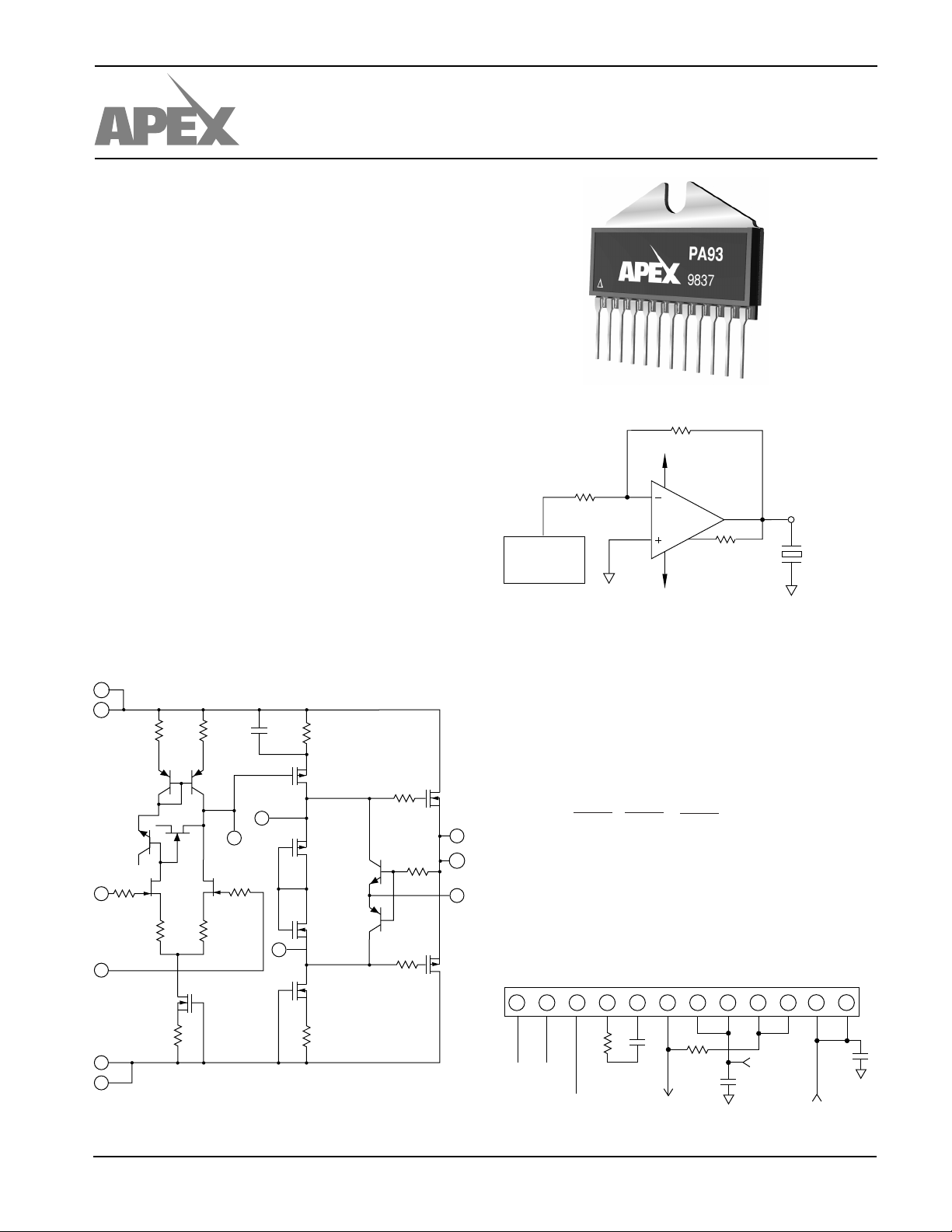
TYPICAL APPLICATION
R
F
+V
S
R
IN
COMPUTER
FOCUS
COMMAND
VOLTAGE
LOW POWER, PIEZOELECTRIC POSITIONING
11,12
1
9,10
6
R
CL
PA93
2
7,8
–V
S
PIEZO DRIVE
V
OUT
EQUIVALENT SCHEMATIC
12
11
+V
–IN
+IN
–V
S
1
2
S
7
8
R1 R2 C1 R3
Q1 Q2
Q6
Q5
R5
R8 R9
Q15
R11 R12
4
CC1
CC2
R6
Piezo positioning may be applied to the focusing of segmented mirror systems. The composite mirror may be composed of hundreds of elements, each requiring focusing under
computer control. In such complex systems the PA93 reduces
the costs of power supplies and cooling with its advantages of
low cost and low quiescent power consumption while increasing circuit density with the SIP package.
Q3
5
Q8
Q11
Q13
Q12
3
I
Q
Q16
R4
R10
R7
Q4
ILIM
9
10
6
OUT
Q14
PHASE COMPENSATION
GAIN
≥1 220pF
≥2
≥4
≥17
*C
Never to be < 10pF. C
c
voltage +V to –Vs. Use ceramic NPO (COG) type.
Cc*R
c
100Ω
100pF
47pF
10pF
100Ω
0Ω
0Ω
To be rated for the full supply
c
EXTERNAL CONNECTIONS Package: SIP03
+V
11
12
*
s
12345678910
–IN +IN
R
I
Q
(See text.)
c
C
c
R
CL
TO LOAD
AND FEEDBACK
–V
*
s
* Bypassing required.
APEX MICROTECHNOLOGY CORPORATION • TELEPHONE (520) 690-8600 • FAX (520) 888-3329 • ORDERS (520) 690-8601 • EMAIL prodlit@apexmicrotech.com
PA93
ABSOLUTE MAXIMUM RATINGS
SPECIFICATIONS
ABSOLUTE MAXIMUM RATINGS
SUPPLY VOLTAGE, +VS to –V
OUTPUT CURRENT, source, sink, peak 14A, within SOA
S
400V
POWER DISSIPATION, continuous @ TC = 25°C 125W
INPUT VOLTAGE, differential ±20V
INPUT VOLTAGE, common mode ±V
TEMPERATURE, pin solder - 10s max 220°C
TEMPERATURE, junction
2
S
150°C
TEMPERATURE, storage –65 to +150°C
OPERATING TEMPERATURE RANGE, case –55 to +125°C
SPECIFICATIONS
PARAMETER TEST CONDITIONS
INPUT
OFFSET VOLTAGE, initial 210mV
OFFSET VOLTAGE, vs. temperature Full temperature range 15 50 µV/°C
OFFSET VOLTAGE, vs. supply 10 25 µV/V
OFFSET VOLTAGE, vs. time 75 µV/√kh
BIAS CURRENT, initial 200 2000 pA
BIAS CURRENT, vs. supply 4 pA/V
OFFSET CURRENT, initial 50 500 pA
INPUT IMPEDANCE, DC 10
INPUT CAPACITANCE 4pF
COMMON MODE VOLTAGE RANGE
3
COMMON MODE REJECTION, DC VCM = ±90V 80 98 dB
NOISE 100KHz BW, RS = 1KΩ, CC = 10pF 1 µVrms
GAIN
OPEN LOOP, @ 15Hz RL = 2KΩ, CC = 10pF 94 111 dB
GAIN BANDWIDTH PRODUCT at 1MHz RL = 2KΩ, CC = 10pF 12 MHz
POWER BANDWIDTH RL = 2KΩ, CC = 10pF 30 kHz
PHASE MARGIN Full temperature range 60 °
OUTPUT
VOLTAGE SWING
3
IO = 8A ±VS 12 ±VS 10 V
CURRENT, continuous 8 A
SLEW RATE, AV = 100 CC = 10pF 50 V/µs
CAPACITIVE LOAD, AV = +1 Full temperature range 1 nf
SETTLING TIME to .1% CC = 10pF, 2V step 1 µs
RESISTANCE, no load 10 Ω
POWER SUPPLY
VOLTAGE
5
See note 5 ±40 ±150 ±200 V
CURRENT, quiescent, 10 14 mA
THERMAL
RESISTANCE, AC, junction to case
4
Full temperature range, F > 60Hz .7 °C/W
RESISTANCE, DC, junction to case Full temperature range, F < 60Hz 1 °C/W
RESISTANCE, junction to air Full temperature range 30 °C/W
TEMPERATURE RANGE, case Meets full range specifications –25 +85 °C
1
MIN TYP MAX UNITS
11
±
±VS 15 V
Ω
±±
NOTES: 1. Unless otherwise noted: TC = 25°C, DC input specifications are ± value given. Power supply voltage is typical rating. RC = 100
CC = 220pF.
2. Long term operation at the maximum junction temperature will result in reduced product life. Derate internal power dissipation
to achieve high MTTF.
3. +VS and –VS denote the positive and negative power supply rail respectively.
4. Rating applies if the output current alternates between both output transistors at a rate faster than 60Hz.
5. Derate max supply rating .625 V/°C below 25°C case. No derating needed above 25°C case.
CAUTION
APEX MICROTECHNOLOGY CORPORATION • 5980 NORTH SHANNON ROAD • TUCSON, ARIZONA 85741 • USA • APPLICATIONS HOTLINE: 1 (800) 546-2739
The PA93 is constructed from MOSFET transistors. ESD handling procedures must be observed.

TYPICAL PERFORMANCE
GRAPHS
P A93
125
POWER DERATING
100
75
50
25
INTERNAL POWER DISSIPATION
0
0 25 50 75 100 125
CASE TEMPERATURE, T (°C )
C
SMALL SIGNAL RESPONSE
50
40
30
20
10
0
OPEN LOOP GAIN, A (dB)
–10
100K
Cc = 220 pF
Cc = 100 pF
Cc = 47 pF
Cc = 10 pF
1M 10M
FREQUENCY, F (Hz)
SLEW RATE
60
40
30
20
µ
10
8
6
4
3
SLEW RATE, (V/ S)
2
1
10 60
EXT. COMPENSATION CAPACITOR, C (pF)
30
100 200 30020 40
CURRENT LIMIT
8
C
PHASE RESPONSE
90
135
Φ
180
Cc = 220 pF
Cc = 100 pF
PHASE, (°)
Cc = 47 pF
225
Cc = 10 pF
270
100k
OUTPUT VOLTAGE SWING
9
SO
8
1M 10M
FREQUENCY F (Hz)
Q
1.8
1.6
1.4
1.2
1.0
NORMALIZED QUIESCENT CURRENT, I (X)
400
PP
O
100
7
6
OUTPUT VOLTAGE, V (V )
5
068
2
OUTPUT CURRENT, I (A)
VOLTAGE DROP FROM SUPPLY, V – V (V)
HARMONIC DISTORTION
.1
Po = 1W
Po = 20W
Po = 62W
4
O
20
15
N
10
.01
DISTORTION, (%)
.001
100 1K
10K
INPUT NOISE VOLTAGE, V (nV Hz)
FREQUENCY, F (Hz)
NORMALIZED QUIES. CURRENT
0 50 100
CASE TEMPERATURE, Tc (°C)
75
POWER RESPONSE
C = 10pF
C
C = 47pF
C
C = 100pF
C
C = 220pF
C
10
1K 10K
FREQUENCY, F (Hz)
100K
INPUT NOISE VOLTAGE
7
5
3
2
10 100 10K 100K
1K
FREQUENCY, F (Hz)
125
1M
6
LIM
4
2
CURRENT LIMIT, I (A)
0
0.2.3.5.6
.1 .4
RESISTOR VALUE, R (Ω)
CL
APEX MICROTECHNOLOGY CORPORATION • TELEPHONE (520) 690-8600 • FAX (520) 888-3329 • ORDERS (520) 690-8601 • EMAIL prodlit@apexmicrotech.com

PA93
OPERATING
CONSIDERATIONS
GENERAL
Please read the “General Operating Considerations” section, which covers stability, supplies, heatsinking, mounting,
current limit, SOA interpretation, and specification interpretation. Additional information can be found in the application
notes. For information on the package outline, heatsinks, and
mounting hardware, consult the “Accessory and Package
Mechanical Data” section of the handbook.
CURRENT LIMIT
For proper operation, the current limit resistor (RCL) must be
connected as shown in the external connection diagram. For
optimum reliability the resistor value should be set as high as
possible. The value is calculated as follows; with the maximum
practical value of 16 ohms.
R
CL
.65
=
I
LIM
SAFE OPERATING AREA (SOA)
The MOSFET output stage of this power operational amplifier has two distinct limitations:
1. The current handling capability of the MOSFET geometry
and the wire bonds.
2. The junction temperature of the output MOSFETs.
NOTE: The output stage is protected against transient flyback.
However, for protection against sustained, high energy flyback,
external fast-recovery diodes should be used.
SAFE OPERATING CURVES
The safe operating area curves define the maximum additional internal power dissipation the amplifier can tolerate
when it produces the necessary output to drive an external
load.
20
10
, (A)
OR –V
OUTPUT CURRENT FROM +V
8
S
6
4
S
3
2
1
.8
.6
.4
.3
.2
.1
.08
.06
10 20 30 40 100 200 300 500
DC, TC = 25°C
DC,T
200mS
DC,T
C
= 125°C
60 80
C
= 85°C
100mS
INPUT PROTECTION
Although the PA93 can withstand differential voltages up to
±20V, additional external protection is recommended. Low
leakage, low capacitance JFETs connected as diodes are
recommended (e.g. 2N4416, Q1-Q4 in Figure 2). The differential input voltage will be clamped to ±1.4V. This is sufficient
overdrive to produce maximum power bandwidth.
POWER SUPPLY PROTECTION
Unidirectional zener diode transient suppressors are recommended as protection on the supply pins. See Figure 2. The
zeners clamp transients to voltages within the power supply
rating and also clamp power supply reversals to ground.
Whether the zeners are used or not, the system power supply
should be evaluated for transient performance including poweron overshoot and power-off polarity reversals as well as line
regulation.
Conditions which can cause open circuits or polarity reversals on either power supply rail should be avoided or protected
against. Reversals or opens on the negative supply rail is
known to induce input stage failure. Unidirectional transzorbs
prevent this, and it is desirable that they be both electrically and
physically as close to the amplifier as possible.
STABILITY
The PA93 is externally compensated and performance can
be tailored to the application. Use the graphs of small signal
response and power response as a guide. The compensation
capacitor C
capacitor is recommended. The compensation network C
must be rated at 500V working voltage. An NPO
C
CRC
must be mounted closely to the amplifier pins 4 and 5 to avoid
spurious oscillation.
QUIESCENT CURRENT REDUCTION
When pin 3 (IQ) is shorted to pin 5 (CC2) the AB biasing of
the output stage is disabled. This lowers quiescent power but
also raises distortion since the output stage is then class C
biased. The output stage bias current is nominally set at 1mA.
Pin 3 may be left open if not used.
+V
S
Z1
1
–IN
Q1
Q2
+IN
FIGURE 2.
OVERVOLTAGE
PROTECTION
Q3
Q4
11, 12
PA93
7, 8
2
–V
S
6
Z2
SUPPLY TO OUTPUT DIFFERENTIAL, VS – VO (V)
This data sheet has been carefully checked and is believed to be reliable, however, no responsibility is assumed for possible inaccuracies or omissions. All specifications are subject to change without notice.
PA93U REV. B MARCH 1999 © 1999 Apex Microtechnology Corp.
 Loading...