Apex PA92 Datasheet

MICROTECHNOLOGY
HTTP://WWW.APEXMICROTECH.COM (800) 546-APEX (800) 546-2739
FEATURES
• HIGH VOLTAGE — 400V (±200V)
• LOW QUIESCENT CURRENT — 10mA
• HIGH OUTPUT CURRENT — 4A
• PROGRAMMABLE CURRENT LIMIT
HIGH VOLTAGE POWER OPERATIONAL AMPLIFIER
PA92
APPLICATIONS
• PIEZOELECTRIC POSITIONING
• HIGH VOLTAGE INSTRUMENTATION
• ELECTROSTATIC TRANSDUCERS
• PROGRAMMABLE POWER SUPPLIES UP TO 390V
DESCRIPTION
The PA92 is a high voltage, low quiescent current MOSFET
operational amplifier designed as a low cost solution for driving
continuous output currents up to 4A and pulse currents up to
7A. The safe operating area (SOA) has no second breakdown
limitations and can be observed for all type loads by choosing
an appropriate current limiting resistor. The MOSFET output
stage is biased AB for linear operation. External compensation
provides flexibility in choosing bandwidth and slew rate for the
application. APEX’s Power SIP package uses a minimum of
board space allowing for high density circuit boards.
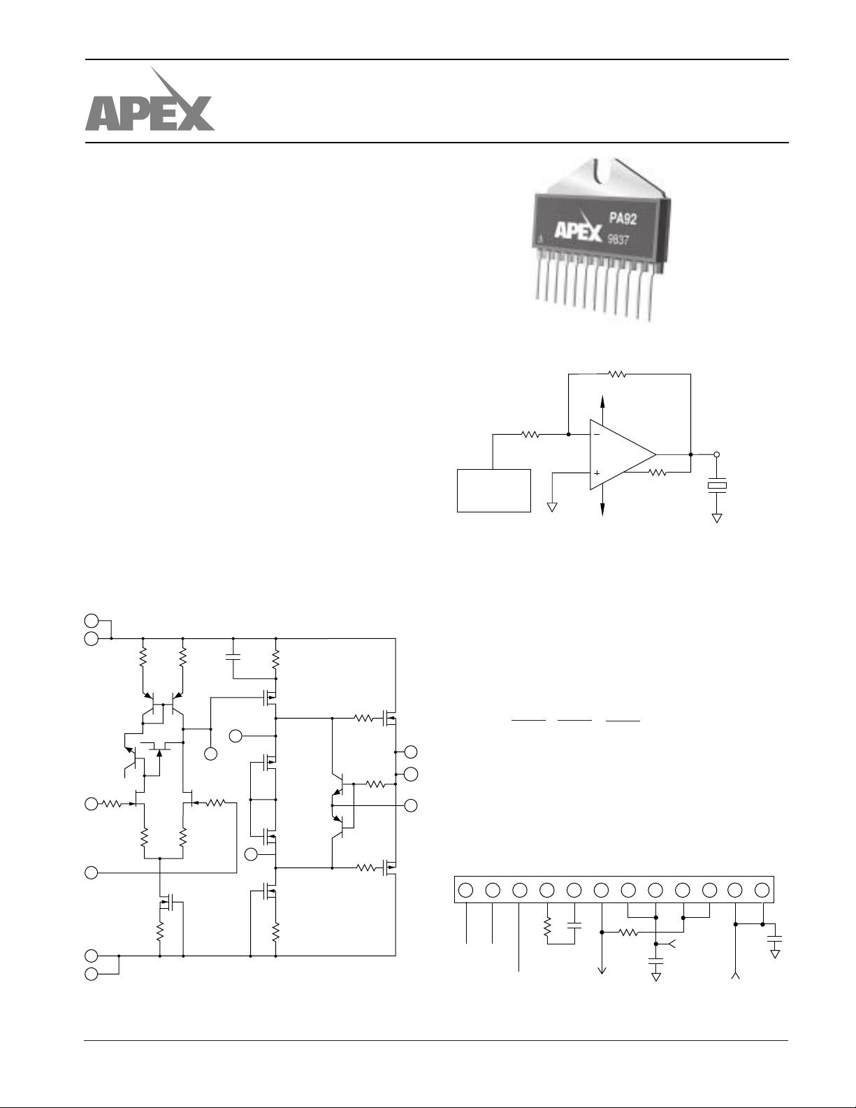
EQUIVALENT SCHEMATIC
12
11
+V
–IN
+IN
–V
S
1
2
S
7
8
R1 R2 C1 R3
Q1 Q2
Q6
Q5
R5
R8 R9
Q15
R11 R12
4
CC1
5
CC2
R6
Q3
Q8
Q11
Q13
Q12
3
I
Q
Q16
R4
R10
Q4
ILIM
R7
OUT
Q14
PATENTED
TYPICAL APPLICATION
R
F
+V
S
11,12
1
PA92
2
9,10
7,8
–V
S
R
6
CL
PIEZO DRIVE
V
OUT
COMPUTER
FOCUS
COMMAND
VOLTAGE
R
IN
LOW POWER, PIEZOELECTRIC POSITIONING
Piezo positioning may be applied to the focusing of segmented mirror systems. The composite mirror may be composed of hundreds of elements, each requiring focusing under
computer control. In such complex systems the PA92 reduces
the costs of power supplies and cooling with its advantages of
low cost and low quiescent power consumption while increasing circuit density with the SIP package.
PHASE COMPENSATION
GAIN
≥1 150pF
9
10
*C
6
c
voltage +V to –Vs. Use ceramic NPO (COG) type.
≥2
≥3
≥12
Never to be < 10pF. C
Cc*R
c
100Ω
100pF
47pF
10pF
100Ω
0Ω
0Ω
To be rated for the full supply
c
EXTERNAL CONNECTIONS Package: SIP03
+V
11
12
*
s
12345678910
–IN +IN
R
I
Q
(See text.)
c
C
c
R
CL
TO LOAD
AND FEEDBACK
–V
*
s
* Bypassing required.
APEX MICROTECHNOLOGY CORPORATION • TELEPHONE (520) 690-8600 • FAX (520) 888-3329 • ORDERS (520) 690-8601 • EMAIL prodlit@apexmicrotech.com

PA92
ABSOLUTE MAXIMUM RATINGS
SPECIFICATIONS
ABSOLUTE MAXIMUM RATINGS
SUPPLY VOLTAGE, +VS to –V
OUTPUT CURRENT, source, sink, peak 7A, within SOA
S
400V
POWER DISSIPATION, continuous @ TC = 25°C 80W
INPUT VOLTAGE, differential ±20V
INPUT VOLTAGE, common mode ±V
TEMPERATURE, pin solder - 10s max 220°C
TEMPERATURE, junction
2
S
150°C
TEMPERATURE, storage –65 to +150°C
OPERATING TEMPERATURE RANGE, case –55 to +125°C
SPECIFICATIONS
PARAMETER TEST CONDITIONS
INPUT
OFFSET VOLTAGE, initial 210mV
OFFSET VOLTAGE, vs. temperature Full temperature range 15 50 µV/°C
OFFSET VOLTAGE, vs. supply 10 25 µV/V
OFFSET VOLTAGE, vs. time 75 µV/√kh
BIAS CURRENT, initial 200 2000 pA
BIAS CURRENT, vs. supply 4 pA/V
OFFSET CURRENT, initial 50 500 pA
INPUT IMPEDANCE, DC 10
INPUT CAPACITANCE 4pF
COMMON MODE VOLTAGE RANGE
3
COMMON MODE REJECTION, DC VCM = ±90V 80 98 dB
NOISE 100KHz BW, RS = 1KΩ, CC = 10pF 1 µVrms
GAIN
OPEN LOOP, @ 15Hz RL = 2KΩ, CC = 10pF 94 111 dB
GAIN BANDWIDTH PRODUCT at 1MHz RL = 2KΩ, CC = 10pF 18 MHz
POWER BANDWIDTH RL = 2KΩ, CC = 10pF 30 kHz
PHASE MARGIN Full temperature range 60 °
OUTPUT
VOLTAGE SWING
3
IO = 4A ±VS 12 ±VS 10 V
CURRENT, continuous 4 A
SLEW RATE, AV = 100 CC = 10pF 50 V/µs
CAPACITIVE LOAD, AV = +1 Full temperature range 1 nf
SETTLING TIME to .1% CC = 10pF, 2V step 1 µs
RESISTANCE, no load 10 Ω
POWER SUPPLY
VOLTAGE
5
See note 5 ±50 ±150 ±200 V
CURRENT, quiescent, 10 14 mA
THERMAL
RESISTANCE, AC, junction to case
4
Full temperature range, F > 60Hz 1 °C/W
RESISTANCE, DC, junction to case Full temperature range, F < 60Hz 1.5 °C/W
RESISTANCE, junction to air Full temperature range 30 °C/W
TEMPERATURE RANGE, case Meets full range specifications –25 +85 °C
1
MIN TYP MAX UNITS
11
±
±VS 15 V
±
±
Ω
NOTES: 1. Unless otherwise noted: TC = 25°C, DC input specifications are ± value given. Power supply voltage is typical rating. RC = 100
CC = 150pF.
2. Long term operation at the maximum junction temperature will result in reduced product life. Derate internal power dissipation
to achieve high MTTF.
3. +VS and –VS denote the positive and negative power supply rail respectively.
4. Rating applies if the output current alternates between both output transistors at a rate faster than 60Hz.
5. Derate max supply rating .625 V/°C below 25°C case. No derating needed above 25°C case.
CAUTION
APEX MICROTECHNOLOGY CORPORATION • 5980 NORTH SHANNON ROAD • TUCSON, ARIZONA 85741 • USA • APPLICATIONS HOTLINE: 1 (800) 546-2739
The PA92 is constructed from MOSFET transistors. ESD handling procedures must be observed.
 Loading...