

HIGH VOLTAGE POWER OPERATIONAL AMPLIFIERS
MICROTECHNOLOGY
HTTP://WWW.APEXMICROTECH.COM (800) 546-APEX (800) 546-2739
FEATURES
• LOW BIAS CURRENT, LOW NOISE — FET Input
• FULLY PROTECTED INPUT — Up to ±150V
• WIDE SUPPLY RANGE — ±15V to ±150V
APPLICATIONS
• HIGH VOLTAGE INSTRUMENTATION
• ELECTROSTATIC TRANSDUCERS & DEFLECTION
• PROGRAMMABLE POWER SUPPLIES UP TO 290V
• ANALOG SIMULATORS
DESCRIPTION
The PA83 is a high voltage operational amplifier designed
for output voltage swings up to ±145V with a dual (±) supply or
290V with a single supply. Its input stage is protected against
transient and steady state overvoltages up to and including the
supply rails. High accuracy is achieved with a cascode input
circuit configuration. All internal biasing is referenced to a
zener diode fed by a FET constant current source. As a result,
the PA83 features an unprecedented supply range and excellent supply rejection. The output stage is biased in the class A/
B mode for linear operation. Internal phase compensation
assures stability at all gain settings without need for external
components. Fixed current limits protect these amplifiers
against shorts to common at supply voltages up to 120V. For
operation into inductive loads, two external flyback pulse
protection diodes are recommended. However, a heatsink
may be necessary to maintain the proper case temperature
under normal operating conditions.
This hybrid circuit utilizes beryllia (BeO) substrates, thick
(cermet) film resistors, ceramic capacitors and silicon semiconductor chips to maximize reliability, minimize size and give
top performance. Ultrasonically bonded aluminum wires provide reliable interconnections at all operating temperatures.
The 8-pin TO-3 package is hermetically sealed and electrically
isolated. The use of compressible thermal isolation washers
and/or improper mounting torque voids product warranty.
Please see Application Note 1 “General Operating Considerations”.
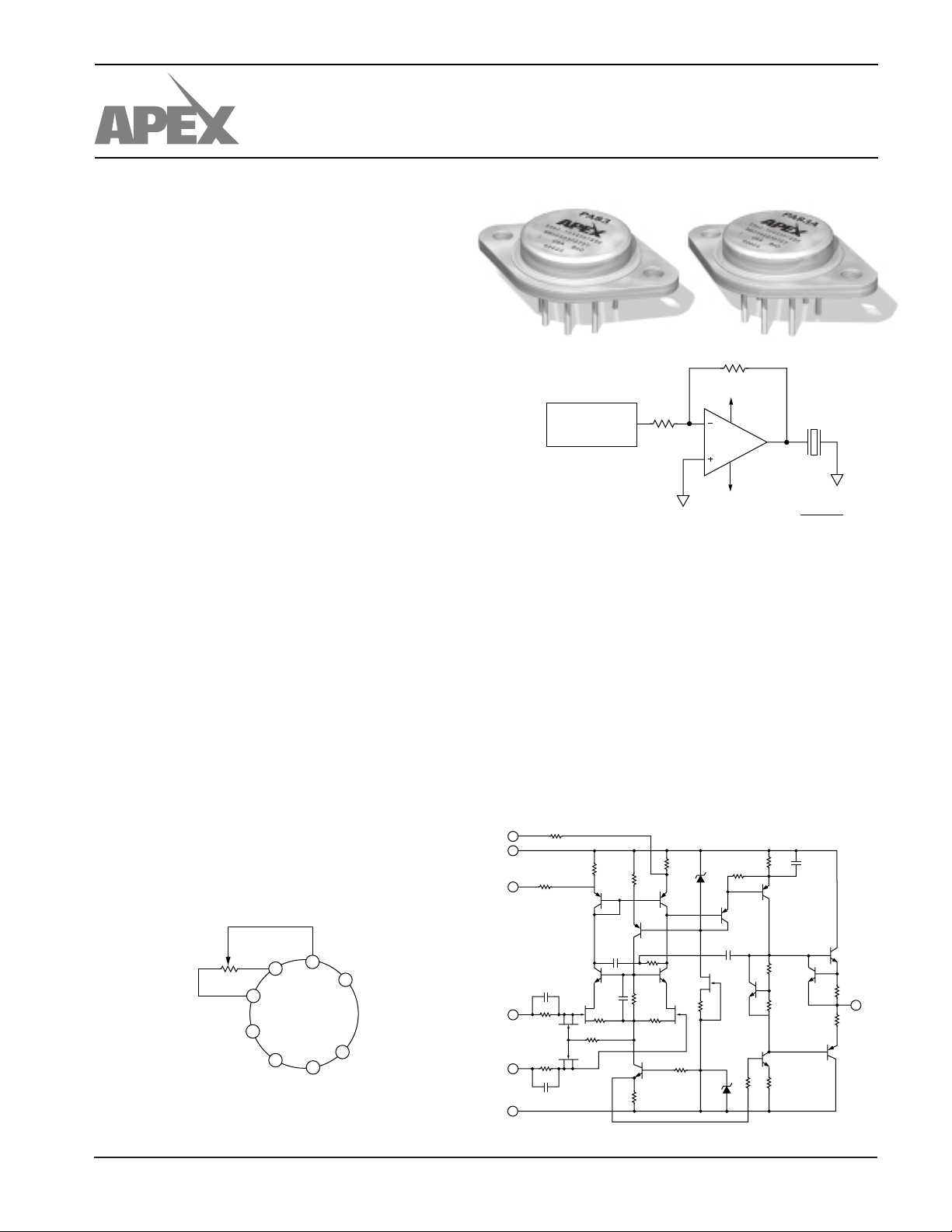
EXTERNAL CONNECTIONS
+V
BAL
BAL
4
–IN
5
NOTES:
+IN
1. Pin 8 not internally connected.
2. Input offset trimpot optional.
Recommended value 100K .Ω
S
2
3
TOP VIEW
6
7
–V
S
1
8
N.C.
OUTPUT
PA83 • PA83A
GATED
OSCILLATOR
SIMPLE PIEZO ELECTRIC TRANSDUCER DRIVE
TYPICAL APPLICATION
While piezo electric transducers present a complex impedance, they are often primarily capacitive at useful frequencies.
Due to this capacitance, the speed limitation for a given
transducer/amplifier combination may well stem from limited
current drive rather than power bandwidth restrictions. With its
drive capability of 75mA, the PA83 can drive transducers
having up to 2nF of capacitance at 40kHz at maximum output
voltage. In the event the transducer may be subject to shock
or vibration, flyback diodes, voltage clamps or other protection
networks must be added to protect the amplifier from high
voltages which may be generated.
EQUIVALENT SCHEMATIC
4
2
3
5
6
7
Q1
Q5
C2
Q8
C5
C6
C4
Q12A
Q13
Q14
Q15
3.57K
±5V
Q2
Q9
Q12B
Q10
100K
+150V
A1
PA83
–150V
D1
Q4
C3
Q11
D2
Q3
Q16
I =
V * C
∆
t
∆
C1
Q7
Q6
1
Q17
APEX MICROTECHNOLOGY CORPORATION • TELEPHONE (520) 690-8600 • FAX (520) 888-3329 • ORDERS (520) 690-8601 • EMAIL prodlit@apexmicrotech.com
PA83 • PA83A
ABSOLUTE MAXIMUM RATINGS
SPECIFICATIONS
ABSOLUTE MAXIMUM RATINGS
SUPPLY VOLTAGE, +VS to –V
OUTPUT CURRENT, within SOA Internally Limited
S
300V
POWER DISSIPATION, internal at TC = 25°C117.5W
INPUT VOLTAGE, differential ±300V
INPUT VOLTAGE, common mode ±300V
TEMPERATURE, pin solder - 10s max (solder) 300°C
TEMPERATURE, junction 150°C
TEMPERATURE RANGE, storage –65 to +150°C
OPERATING TEMPERATURE RANGE, case –55 to +125°C
SPECIFICATIONS
PARAMETER TEST CONDITIONS
PA83
2
MIN TYP MAX MIN TYP MAX UNITS
PA83A
INPUT
OFFSET VOLTAGE, initial TC = 25°C ±1.5 ±3 ±.5 ±1mV
OFFSET VOLTAGE, vs. temperature Full temperature range ±10 ±25 ±5 ±10 µV/°C
OFFSET VOLTAGE, vs. supply TC = 25°C ±.5 ±.2 µV/V
OFFSET VOLTAGE, vs. time TC = 25°C ±75 * µV/√kh
BIAS CURRENT, initial
BIAS CURRENT, vs. supply TC = 25°C .01 * pA/V
OFFSET CURRENT, initial
OFFSET CURRENT, vs. supply TC = 25°C ±.01 * pA/V
INPUT IMPEDANCE, DC TC = 25°C10
3
3
TC = 25°C550310pA
TC = 25°C ±2.5 ±50 ±1.5 ±10 pA
11
* Ω
INPUT CAPACITANCE Full temperature range 6 * pF
COMMON MODE VOLTAGE RANGE4Full temperature range ±VS–10 * V
COMMON MODE REJECTION, DC Full temperature range 130 * dB
GAIN
OPEN LOOP GAIN at 10Hz TC = 25°C, RL = 2KΩ 96 116 * * dB
UNITY GAIN CROSSOVER FREQ. TC = 25°C, RL = 2KΩ 5 3 * MHz
POWER BANDWIDTH TC = 25°C, RL = 10KΩ 60 40 * kHz
PHASE MARGIN Full temperature range 60 * °
OUTPUT
VOLTAGE SWING4, full load Full temp. range, IO = 75mA ±VS–10 ±VS–5** V
VOLTAGE SWING
4
Full temp. range, IO = 15mA ±VS–5 ±VS–3** V
CURRENT, peak TC = 25°C75*mA
CURRENT, short circuit TC = 25°C 100 * mA
SLEW RATE
6
TC = 25°C, RL = 2KΩ 20 30 * * V/µs
CAPACITIVE LOAD, unity gain Full temperature range 10 * nF
CAPACITIVE LOAD, gain > 4 Full temperature range SOA * µF
SETTLING TIME to .1% TC = 25°C, RL = 2KΩ, 10V step 12 * µs
POWER SUPPLY
VOLTAGE TC = –55°C to +125°C ±15 ±150 ±150 * * * V
CURRENT, quiescent TC = 25°C 6 8.5 * * mA
THERMAL
RESISTANCE, AC, junction to case
5
F > 60Hz 3.8 * °C/W
RESISTANCE, DC, junction to case F < 60Hz 6 6.5 * * °C/W
RESISTANCE, case to air 30 * °C/W
TEMP. RANGE, case (PA83/PA83A) Meets full range specification –25 +85 * * °C
TEMP. RANGE, case (PA83J) Meets full range specification 0 70 °C
NOTES: * The specification of PA83A is identical to the specification for PA83 in applicable column to the left.
1. Long term operation at the maximum junction temperature will result in reduced product life. Derate internal power dissipation
to achieve high MTTF.
2. The power supply voltage for all tests is the TYP rating, unless otherwise noted as a test condition.
3. Doubles for every 10°C of temperature increase.
4. +VS and –VS denote the positive and negative supply rail respectively. Total VS is measured from +VS to –VS.
5. Rating applies if the output current alternates between both output transistors at a rate faster than 60Hz.
6. Signal slew rates at pins 5 and 6 must be limited to less than 1V/ns to avoid damage. When faster waveforms are unavoidable,
resistors in series with those pins, limiting current to 150mA will protect the amplifier from damage.
CAUTION
APEX MICROTECHNOLOGY CORPORATION • 5980 NORTH SHANNON ROAD • TUCSON, ARIZONA 85741 • USA • APPLICATIONS HOTLINE: 1 (800) 546-2739
The internal substrate contains beryllia (BeO). Do not break the seal. If accidentally broken, do not crush, machine, or
subject to temperatures in excess of 850°C to avoid generating toxic fumes.
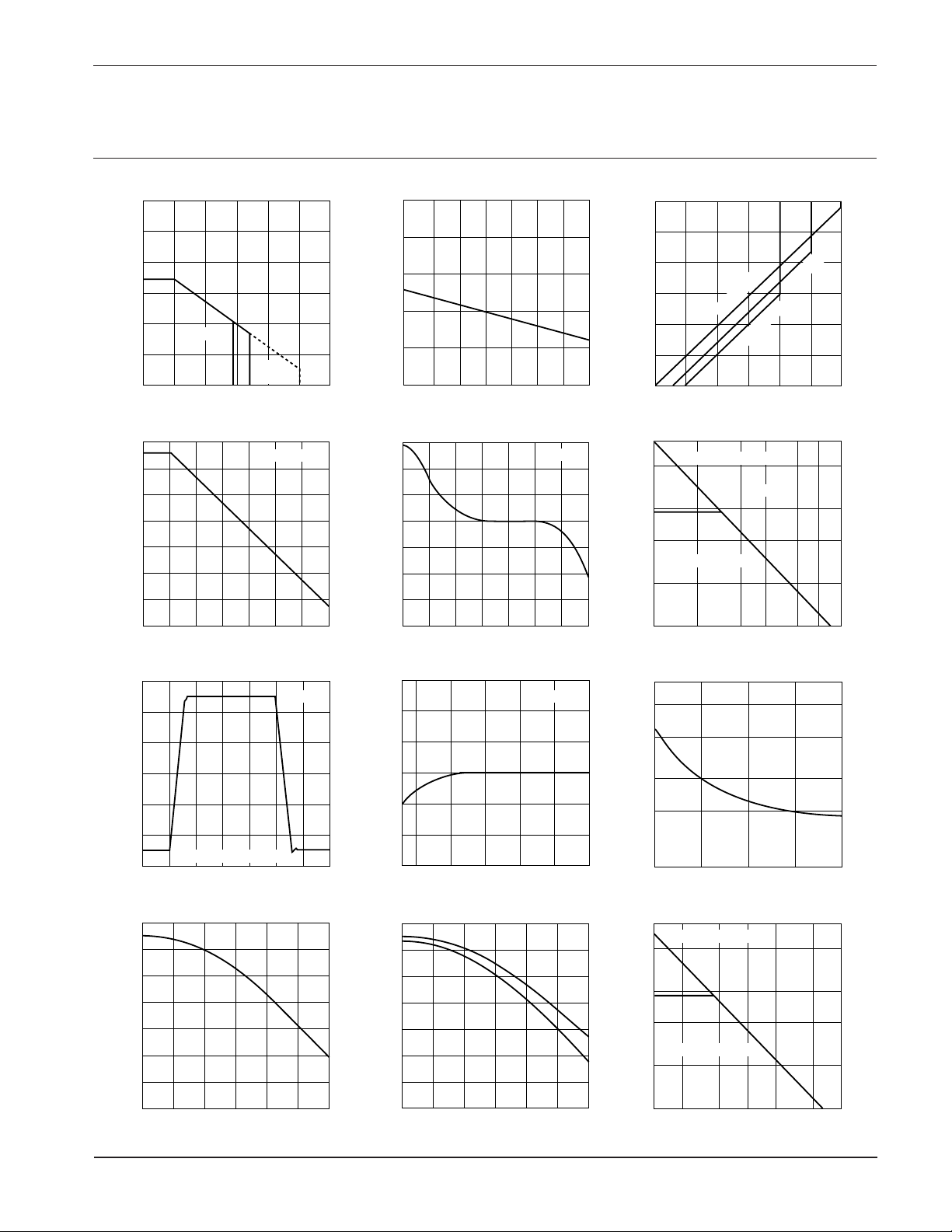
TYPICAL PERFORMANCE
GRAPHS
PA83 • PA83A
30
POWER DERATING
25
20
15
10
PA83J
5
PA83/
0
0 25 50 75 100 125
INTERNAL POWER DISSIPATION, P (W)
120
TEMPERATURE, T (°C)
SMALL SIGNAL RESPONSE
100
(dB)
80
OL
PA83A
RL = 2K Ω
60
40
20
0
OPEN LOOP GAIN, A
–20
1
10010
1K 100K
10K 1M 10M
FREQUENCY, F (Hz)
PULSE RESPONSE
)
(V
6
P
4
O
RL = 2K Ω RL = 2K Ω
2
150
CURRENT LIMIT
(A)
250
200
LIM
150
100
50
CURRENT LIMIT, I
0
–55 100
–25 25 50 75
0
CASE TEMPERATURE, TC (°C) OUTPUT CURRENT I
PHASE RESPONSE
0
–30
–60
–90
Φ
–120
PHASE, (°)
–150
–180
–210
10
1
100
1K 10K
FREQUENCY, F (Hz)
SLEW RATE VS. SUPPLY
1.6
1.4
1.2
RL = 2K Ω
.1M
1M
(V)
OUTPUT VOLTAGE SWING
O
8
–V
S
7
6
5
4
3
2
125
0 60 100
VOLTAGE DROP FROM SUPPLY, V
300
200
PP
O
100
60
| +VS | + | –VS | = 100V
30
OUTPUT VOLTAGE, V (V )
15
10M
50K
20
√
15
(nV/ Hz)
N
10
= –25°C
C
T
= 85°C
C
T
20 40 80
O
POWER RESPONSE
| +VS | + | –VS | = 300V
RL = 2K Ω
.1M
.2M .5M
.3M
FREQUENCY, F (Hz)
INPUT NOISE
= 25
C
T
(mA)
.7M
°C
120
1M
0
–2
–4
OUTPUT VOLTAGE, V
–6
–.5
140
VIN = ±5V, tr =100ns
.5 1.5 2.51
0 2.0
TIME, t (µs)
COMMON MODE REJECTION
120
100
80
60
40
20
0
1
COMMON MODE REJECTION, CMR (dB)
10 100
FREQUENCY, F (Hz)
1K
10K
.1M
3.0
1M
1.0
.8
.6
NORMALIZED SLEW RATE (X)
.4
3050 100 150
TOTAL SUPPLY VOLTAGE, V
POWER SUPPLY REJECTION
140
200
250 300
(V)
S
120
100
80
+V
60
40
–V
20
0
POWER SUPPLY REJECTION, PSR (dB)
10 100
1
FREQUENCY, F (Hz)
1K 10K 1M
.1M
6
4
2
INPUT NOISE VOLTAGE, V
10 1K 10K
100
.1M
FREQUENCY, F (Hz)
COMMON MODE VOLTAGE
)
300
PP
| +VS | + | –VS | = 300V
(V
200
CM
100
S
60
| +VS | + | –VS | = 100V
S
30
15
COMMON MODE VOLTAGE, V
10K
20K
50K
.1M
.2M .5M
1M
FREQUENCY, F (Hz)
APEX MICROTECHNOLOGY CORPORATION • TELEPHONE (520) 690-8600 • FAX (520) 888-3329 • ORDERS (520) 690-8601 • EMAIL prodlit@apexmicrotech.com
PA83 • PA83A
)
GENERAL
Please read Application Note 1, which covers stability,
supplies, heatsinking, mounting, current limit, SOA interpretation, and specification interpretation. Additional information
can be found in the application notes. For information on the
package outline, heatsinks, and mounting hardware, consult
the “Accessory and Package Mechanical Data” section of the
handbook.
SAFE OPERATING AREA (SOA)
The bipolar output stage of this high voltage amplifier has
two distinct limitations.
1. The internal current limit, which limits maximum available
output current.
2. The second breakdown effect, which occurs whenever the
simultaneous collector current and collector-emitter voltage
exceed specified limits.
200
150
(mA)
S
INTERNAL CURRENT LIMIT
100
OR –V
S
70
50
SECOND BREAKDO
steady state
t = 1ms
t = 5ms
t = 0.5m
W
N
s
OPERATING
CONSIDERATIONS
4. The output stage is protected against transient flyback.
However, for protection against sustained, high energy
flyback, external fast-recovery diodes should be used.
INDUCTIVE LOADS
Two external diodes as shown in Figure 1, are required to
protect these amplifiers against flyback (kickback) pulses
exceeding the supply voltages of the amplifier when driving
inductive loads. For component selection, these external
diodes must be very quick, such as ultra fast recovery diodes
with no more than 200 nanoseconds of reverse recovery time.
Be sure the diode voltage rating is greater than the total of both
supplies. The diode will turn on to divert the flyback energy into
the supply rails thus protecting the output transistors from
destruction due to reverse bias.
A note of caution about the supply. The energy of the flyback
pulse must be absorbed by the power supply. As a result, a
transient will be superimposed on the supply voltage, the
magnitude of the transient being a function of its transient
impedance and current sinking capability. If the supply voltage
plus transient exceeds the maximum supply rating or if the AC
impedance of the supply is unknown, it is best to clamp the
output and the supply with a zener diode to absorb the
transient.
+V
S
40
30
OUTPUT CURRENT FROM +V
20
80
100 300
INTERNAL VOLTAGE DROP, SUPPLY TO OUTPUT (V
150120
200
250
The SOA curves combine the effect of these limits. For a
given application, the direction and magnitude of the output
current should be calculated or measured and checked against
the SOA curves. This is simple for resistive loads but more
complex for reactive and EMF generating loads. However, the
following guidelines may save extensive analytical efforts:
1. The following capacitive and inductive loads are safe:
±V
S
C(MAX) L(MAX)
150V .7 F 1.5H
125V 2.0µF 2.5H
100V 5.µF 6.0H
75V 60µF 30H
50V ALL ALL
2. Short circuits to ground are safe with dual supplies up to
120V or single supplies up to 120V.
3. Short circuits to the supply rails are safe with total supply
voltages up to 120V, e.g. ±60V.
–V
S
FIGURE 1. PROTECTION, INDUCTIVE LOAD
This data sheet has been carefully checked and is believed to be reliable, however, no responsibility is assumed for possible inaccuracies or omissions. All specifications are subject to change without notice.
PA83U REV. M JANUARY 2000 © 2000 Apex Microtechnology Corp.
 Loading...